A HIGH PERFORMANCE CMOS COMPARATOR
CIRCUIT
MOHD SHAMIAN ZAINAL
HOTEL ASEANIA RESORT
A High Performance CMOS Comparator Circuit
Mohd Shamian Bin Zainal, Shipun Anuar Bin Hamzah, Nurul Aziyana Binti Kamaruddin
Faculty o f Electrical and Electronic Engineering Kolej Universiti Teknologi Tun Hussein Onn
86400 Parit Raja Batu Pahat, Johor
Abstract
In this paper, we present a method to design high performance CMOS
comparator circuit with 0.35 //w
technology. The comparator can be divided into three stages. The first stage of the comparator is the preamplifier which is increasing the input sensitivity and isolates the input side from the switching noise originating from the positive feedback stage. The second stage of the comparator is the positive feedback. This stage will determine which of the input signal is larger. The last stage is the output buffer amplifier which will amplifies the information and output a corresponding digital signal. These comparator have high gain with little delay and high slew rate for diving off the chip load capacitance. The simulation result shows that propagation delay and gain is 10ns and 2000.
Introduction
The schematic symbol and basic operation of a voltage comparator are shown in Figure 1. The comparator can be thought of as a decision making circuit. If the positive input of the comparator is at a greater potential than the negative input, the output of the comparator is a logic 1 or high, whereas
if the positive input is at potential less than the negative input, the output of the comparator is a logic 0 or low. The operation like magnitude comparator.
vout =lwhen v+ >v_ (1)
v„u, ~ 0 when v+ <v_ (2)
where
v+ = positive input
v_ = negative input
A magnitude comparator determines the larger of two binary numbers [1].
High Performance Comparator
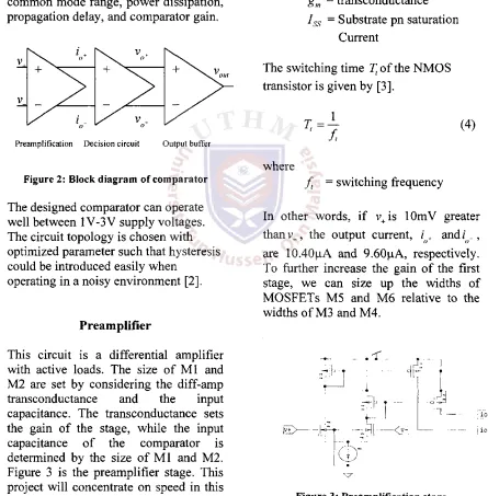
follows by decision stage and output buffer. The preamplifier stage amplifies the input signal to improve the comparator sensitivity and isolates the input of the comparator from switching noise coming from the positive feedback stage. The positive feedback stage is used to determine which of the input signals is larger. The output buffer amplifies this information and outputs a digital signal. Designing a comparator can begin with considering input common mode range, power dissipation, propagation delay, and comparator gain.
Preamplification Decision circuit Output buffer
Figure 2: Block diagram of comparator
The designed comparator can operate well between 1V-3V supply voltages. The circuit topology is chosen with optimized parameter such that hysteresis could be introduced easily when
operating in a noisy environment [2],
Preamplifier
[image:3.595.75.520.238.691.2]This circuit is a differential amplifier with active loads. The size of Ml and M2 are set by considering the diff-amp transconductance and the input capacitance. The transconductance sets the gain of the stage, while the input capacitance of the comparator is determined by the size of Ml and M2. Figure 3 is the preamplifier stage. This project will concentrate on speed in this
design, therefore the channel length of the MOSFETs is 2 jum. Notice that there are no high impedance node in this circuit, other than the input and output nodes. Using the size given in the schematic, the output current can be determined.
V = j y (v + - 0 + y (3)
where
gm = transconductance Is s = Substrate pn saturation
Current
The switching time Tt of the NMOS transistor is given by [3].
1
where
T, = —
f ,
ft = switching frequency (4)
In other words, if v+is lOmV greater
thanv_, the output current, ig+ and / ,
are 1 0 . 4 0 |jA and 9 . 6 0 | A A , respectively.
To further increase the gain of the first stage, we can size up the widths of MOSFETs M5 and M6 relative to the widths of M3 and M4.
[image:3.595.335.531.560.675.2]Decision stage
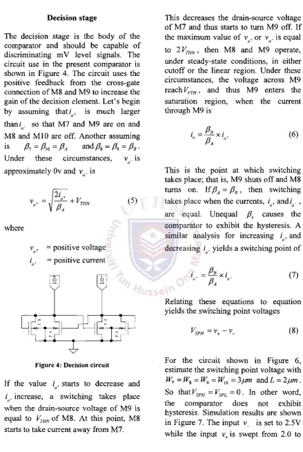
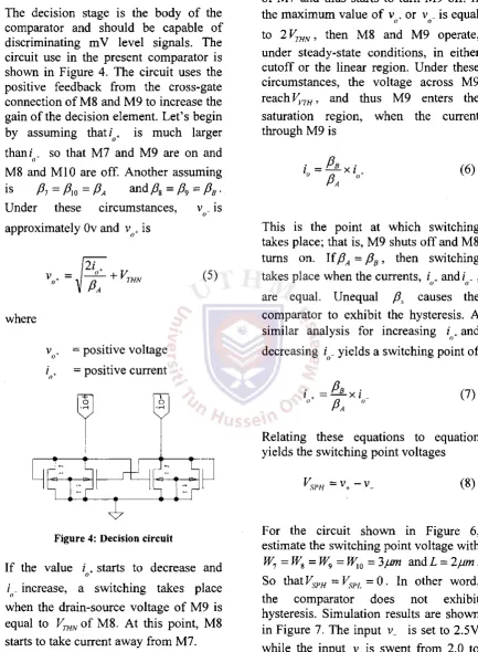
The decision stage is the body of the comparator and should be capable of discriminating mV level signals. The circuit use in the present comparator is shown in Figure 4. The circuit uses the positive feedback from the cross-gate connection of M8 and M9 to increase the gain of the decision element. Let's begin by assuming that ig+ is much larger
than/ _ so that M7 and M9 are on and o
M8 and M10 are off. Another assuming is (31=/3w=/3a m d & = j 39= PB.
Under these circumstances, v _ is
' o
approximately Ov and vo+ is
(5)
where
V
/
+; positive voltage : positive current
T - I
] r U r
[image:4.595.75.515.53.707.2]S I=r
1 , :r
Figure 4: Decision circuit
If the value i +o starts to decrease and
ig. increase, a switching takes place when the drain-source voltage of M9 is equal to VTHN of M8. At this point, M8 starts to take current away from M7.
This decreases the drain-source voltage of M7 and thus starts to turn M9 off. If the maximum value of vo+ or v is equal
to 2 VTHN, then M8 and M9 operate, under steady-state conditions, in either cutoff or the linear region. Under these circumstances, the voltage across M9 reach Vvm, and thus M9 enters the saturation region, when the current through M9 is
• Pb •
Pa °
(6)
This is the point at which switching takes place; that is, M9 shuts off and M8 turns on. I ff iA= f3B, then switching takes place when the currents, / + andz'o_,
are equal. Unequal J3S causes the comparator to exhibit the hysteresis. A similar analysis for increasing / + and
decreasing / _ yields a switching point of
Pb Pa
(7)
Relating these equations to equation yields the switching point voltages
VSPH =V+-V_ (8)
For the circuit shown in Figure 6, estimate the switching point voltage with
Wn = W% = W9 = W10 - 3 jLan a n d L = 2 pim.
3.0V. Note that the amplitudes of vo+ and
vo_ are limited to approximately 2VTHN . All the NMOS in the complete
schematic of comparator are designed via [5]
where
W
j5 = KP x — (9)
KP =50^4 V2
W = width
L = length
Output buffer
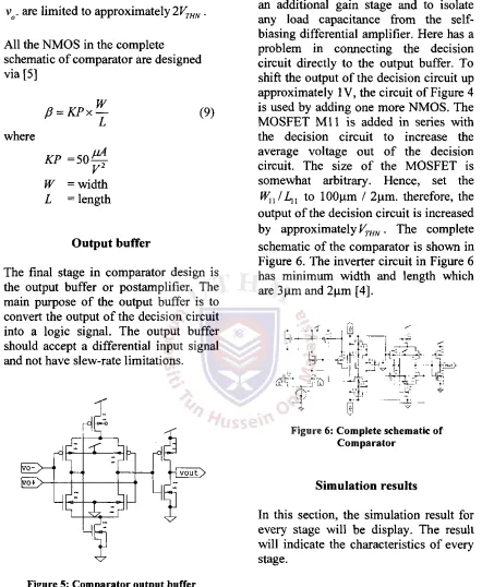
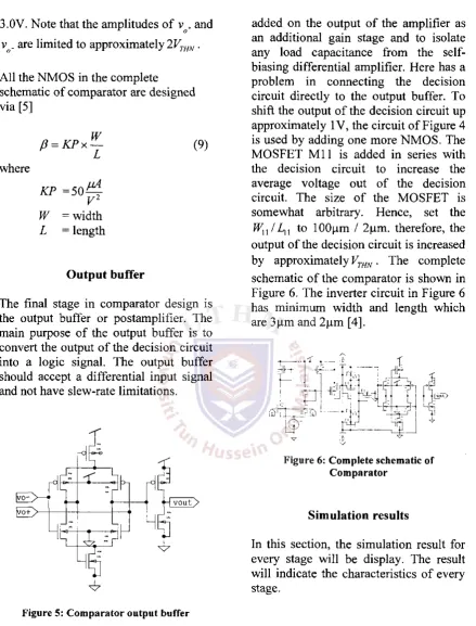
The final stage in comparator design is the output buffer or postamplifier. The main purpose of the output buffer is to convert the output of the decision circuit into a logic signal. The output buffer should accept a differential input signal and not have slew-rate limitations.
H v o u Q
added on the output of the amplifier as an additional gain stage and to isolate any load capacitance from the self-biasing differential amplifier. Here has a problem in connecting the decision circuit directly to the output buffer. To shift the output of the decision circuit up approximately IV, the circuit of Figure 4 is used by adding one more NMOS. The MOSFET M i l is added in series with the decision circuit to increase the average voltage out of the decision circuit. The size of the MOSFET is somewhat arbitrary. Hence, set the
W n l t o 100(am / 2|im. therefore, the output of the decision circuit is increased by approximately VTHN. The complete schematic of the comparator is shown in Figure 6. The inverter circuit in Figure 6 has minimum width and length which are 3(am and 2|im [4].
f l —1 M P
~~' p . r< M i r . r<
M 3 b k p r _L H
Figure 6: Complete schematic of Comparator
Simulation results
[image:5.595.78.520.88.626.2]In this section, the simulation result for every stage will be display. The result will indicate the characteristics of every stage.
Figure 5: Comparator output buffer
O u t p u t V o l t a g e : v o - a n d v o + v - : L o g i c input
I _ _ J I I L
Figure 7: Input v+ swept with v_ at 2.5V
Time <m«)
(b)
The result in Figure 7 show the v+ and
v_ input are swept at 2.5V. This indicates that preamplifier characteristic design without hysteresis.
Input v o l t a g e a n d Logic level
v o u t : o u t p u t level
' f - - |T " . L _ _ L .
i, t
[image:6.595.92.502.67.652.2]-' 1 1 W
Figure 8: Input v+ , v_and logic level
The result in Figure 8 shows the input cross section between input voltage and logic level. voul is high when v+ has a
greater potential than the v_ input.
v + : Logic input
[image:6.595.87.261.76.208.2](c)
Figure 9: Input comparator (a), (b) and logic level (c).
The result in Figure 9(a) and 9(b) shows the logical input with different voltage level. The result in Figure 9(c) is the output of comparator.
200 0 210 0 220 0 230 0 240 0 250 0 260 C
Figure 10: Delay of the comparator
(a)
[image:6.595.316.506.501.642.2] [image:6.595.87.261.544.690.2]indicate the comparator still can be improved by reducing the delay.
i
!
\
/
y I \
[image:7.595.84.271.109.258.2]2 . 4 9 0 2 495 2 5 0 0 2 SOS 2 510
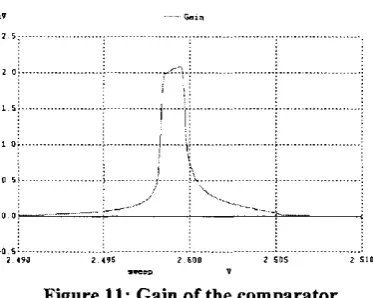
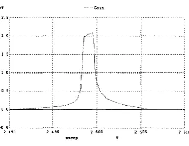
Figure 11: Gain of the comparator
The result in figure 11 shows the gain of the comparator at about 2,000 so that approximately 2.5mV is needed to make the comparator output change logic levels. The comparator gain can be increased by increasing the transconductance of the preamp, that is, by increasing the widths of Ml and M2 or by adding additional inverters.
Conclusion
In this paper we present a method to design high performance CMOS comparator circuit with 3 stages. Every stage is important. The stage performance can be determined by looking the simulation result and calculation. The first stage is important for sensitivity and speed. In other words, to get high sensitivity and speed can be directly improve the preamplifier stage. The channel length should be as small as possible to speed up the circuit [6], At last, the delay of the comparator can be reduced by cascading gain stage.
References
[1] Neil H.E; David Harris, CMOS VLSI Design, Addison Wesley, United State of America, 1998, Third Edition, 2005.
[2] Parlak, M.; Gurbuz, Y., "Low power, variable supply CMOS
comparator", Signal Processing
and Communications Applications Conference, 2004.
Proceedings of the IEEE 12th 2830 April 2004 Page(s):140
-143
[3] Le, H.P.; Zayegh, A.; Singh, J ,
"Performance analysis of optimised CMOS comparator",
Electronics Letters, Volume 39, Issue 11, 29 May 2003 Page(s):833 - 835.R.
[4] Jacob Baker; Harry W.Li;
David E. Boyce, CMOS circuit design, layout and simulation,
John Wiley & Son, Inc., United State of America, 1998.
[5] Steyaert, M.; Comino, V, "High-speed accurate CMOS comparator", Electronics Letters Volume 24, Issue 16, 4 Aug. 1988 Page(s): 1027 - 1028. [6] Wu Rang; Wu Xiaobo; Yan
Xiaolang, "A dynamic CMOS comparator with high precision and resolution ", Solid-State and Integrated Circuits Technology, 2004. Proceedings. 7th
A High Performance CMOS Comparator Circuit
Mohd Shamian Bin Zainal, Shipun Anuar Bin Hamzah, Nurul Aziyana Binti Kamaruddin
Faculty of Electrical and Electronic Engineering Kolej Universiti Teknologi Tun Hussein Onn
86400 Parit Raja Batu Pahat, Johor
Abstract
In this paper, we present a method to design high performance CMOS comparator circuit with 035/jm technology. The comparator can be divided into three stages. The first stage of the comparator is the preamplifier which is increasing the input sensitivity and isolates the input side from the switching noise originating from the positive feedback stage. The second stage of the comparator is the positive feedback. This stage will determine which of the input signal is larger. The last stage is the output buffer amplifier which will amplifies the information and output a corresponding digital signal. These comparator have high gain with little delay and high slew rate for diving off the chip load capacitance. The simulation result shows that propagation delay and gain is 10ns and 2000.
Introduction
The schematic symbol and basic operation of a voltage comparator are shown in Figure 1. The comparator can be thought of as a decision making circuit. If the positive input of the comparator is at a greater potential than the negative input, the output of the comparator is a logic 1 or high, whereas
if the positive input is at potential less than the negative input, the output of the comparator is a logic 0 or low. The operation like magnitude comparator.
vou, =lwhen v+ >v_ (1)
vnut = Owhen v+ < v_ (2)
where
v+ = positive input
v_ = negative input
A magnitude comparator determines the larger of two binary numbers [1].
High Performance Comparator
follows by decision stage and output buffer. The preamplifier stage amplifies the input signal to improve the comparator sensitivity and isolates the input of the comparator from switching noise coming from the positive feedback stage. The positive feedback stage is used to determine which of the input signals is larger. The output buffer amplifies this information and outputs a digital signal. Designing a comparator can begin with considering input common mode range, power dissipation, propagation delay, and comparator gain.
Preamplification Decision circuit Output buffer
Figure 2: Block diagram of comparator
The designed comparator can operate well between 1V-3Y supply voltages. The circuit topology is chosen with optimized parameter such that hysteresis could be introduced easily when
operating in a noisy environment [2].
Preamplifier
[image:9.596.75.521.244.693.2]This circuit is a differential amplifier with active loads. The size of Ml and M2 are set by considering the diff-amp transconductance and the input capacitance. The transconductance sets the gain of the stage, while the input capacitance of the comparator is determined by the size of Ml and M2. Figure 3 is the preamplifier stage. This project will concentrate on speed in this
design, therefore the channel length of the MOSFETs is 2 jam. Notice that there are no high impedance node in this circuit, other than the input and output nodes. Using the size given in the schematic, the output current i<r can be
determined.
+ ^ (3)
where
gm = transconductance Is s = Substrate pn saturation
Current
The switching time Tt of the NMOS transistor is given by [3].
1
where
T,
= f
tft — switching frequency (4)
In other words, if v+is lOmV greater
thanv_, the output current, / + and/'o_,
are 10.40|iA and 9.60|iA, respectively. To further increase the gain of the first stage, we can size up the widths of MOSFETs M5 and M6 relative to the widths of M3 and M4.
s
T T [image:9.596.333.531.559.677.2]Decision stage
The decision stage is the body of the comparator and should be capable of discriminating mV level signals. The circuit use in the present comparator is shown in Figure 4. The circuit uses the positive feedback from the cross-gate connection of M8 and M9 to increase the gain of the decision element. Let's begin by assuming that/'o+ is much larger
than i _ so that M7 and M9 are on and o
M8 and Ml0 are off. Another assuming
is P1 = Ao = PA and PS=P9=PB.
Under these circumstances, v _ is ' o
approximately Ov and vo+ is
2 / +
+ VTHN 7 (5)
where
V positive voltage
: positive current
J
:r J r
J
:Lj
[image:10.595.77.511.94.684.2]1
1
Figure 4: Decision circuit
If the value i +o starts to decrease and
ig_ increase, a switching takes place when the drain-source voltage of M9 is equal to VTHN of M8. At this point, M8 starts to take current away from M7.
This decreases the drain-source voltage of M7 and thus starts to turn M9 off. If the maximum value of v + or v _ is equal
o o 1
to 2 VTHN, then M8 and M9 operate, under steady-state conditions, in either cutoff or the linear region. Under these circumstances, the voltage across M9 reach Vvm, and thus M9 enters the saturation region, when the current through M9 is
• PB • (6)
This is the point at which switching takes place; that is, M9 shuts off and M8 turns on. If = j5B, then switching takes place when the currents, z'o+ and/o_,
are equal. Unequal Ps causes the comparator to exhibit the hysteresis. A similar analysis for increasing z'o+ and
decreasing i . yields a switching point of
Pb •
° PA °
(7)
Relating these equations to equation yields the switching point voltages
VSPH =V+-V_ (8)
For the circuit shown in Figure 6, estimate the switching point voltage with
3.0V. Note that the amplitudes of vo+ and
vo_ are limited to approximately 2VTHN . All the NMOS in the complete
schematic of comparator are designed via [5]
W
P = KP x — (9) where
KP =50*4 V2
W = width
L = length
Output buffer
The final stage in comparator design is the output buffer or postamplifier. The main purpose of the output buffer is to convert the output of the decision circuit into a logic signal. The output buffer should accept a differential input signal and not have slew-rate limitations.
added on the output of the amplifier as an additional gain stage and to isolate any load capacitance from the self-biasing differential amplifier. Here has a problem in connecting the decision circuit directly to the output buffer. To shift the output of the decision circuit up approximately IV, the circuit of Figure 4 is used by adding one more NMOS. The MOSFET M i l is added in series with the decision circuit to increase the average voltage out of the decision circuit. The size of the MOSFET is somewhat arbitrary. Hence, set the
[image:11.596.82.522.57.635.2]Wu I Lu to 100(im / 2|am. therefore, the output of the decision circuit is increased by approximately VTHN. The complete schematic of the comparator is shown in Figure 6. The inverter circuit in Figure 6 has minimum width and length which are 3|am and 2(j.m [4].
Figure 6: Complete schematic of Comparator
Simulation results
In this section, the simulation result for every stage will be display. The result will indicate the characteristics of every stage.
O u t p u t V o l t a g e : vo- a n d v o + v - : Logic input
7r 1 1 ' ' ' '»'-.' ' ' ' ' ' ' '
Vv» (V)
Figure 7: Input v+ swept with v_ at 2.5V
>
!
(b)
The result in Figure 7 show the v+ and
v_ input are swept at 2.5V. This indicates that preamplifier characteristic design without hysteresis.
Input v o l t a g e a n d Logic level
1:
- r i
- i 1
-f-11 A —T. T,— '.'.'
[image:12.596.86.506.62.655.2]W» (V)
Figure 8: Input v+ , v_ and logic level
The result in Figure 8 shows the input cross section between input voltage and logic level. voul is high when v+ has a greater potential than the v_ input.
v * : Logic input
[image:12.596.87.265.78.206.2](C)
Figure 9: Input comparator (a), (b) and logic level (c).
The result in Figure 9(a) and 9(b) shows the logical input with different voltage level. The result in Figure 9(c) is the output of comparator.
/ \
/"""
/
\
/
1 ....
\
i
I
\
\J
v
(a)
2 0 0 . 0 2 1 0 . 0 2 2 0 . 0 2 3 0 . 0 2 4 0 . 0 2 5 0 . 0 260.1
tine nS
Figure 10: Delay of the comparator
[image:12.596.314.506.502.645.2] [image:12.596.87.262.546.692.2]indicate the comparator still can be improved by reducing the delay.
kV Gain
1
[image:13.594.84.270.110.253.2]j 1
Figure 11: Gain of the comparator
The result in figure 11 shows the gain of the comparator at about 2,000 so that approximately 2.5mV is needed to make the comparator output change logic levels. The comparator gain can be increased by increasing the transconductance of the preamp, that is, by increasing the widths of Ml and M2 or by adding additional inverters.
Conclusion
In this paper we present a method to design high performance CMOS comparator circuit with 3 stages. Every stage is important. The stage performance can be determined by looking the simulation result and calculation. The first stage is important for sensitivity and speed. In other words, to get high sensitivity and speed can be directly improve the preamplifier stage. The channel length should be as small as possible to speed up the circuit [6]. At last, the delay of the comparator can be reduced by cascading gain stage.
References
[1] Neil H.E; David Harris, CMOS VLSI Design, Addison Wesley, United State of America, 1998, Third Edition, 2005.
[2] Parlak, M.; Gurbuz, Y., "Low power, variable supply CMOS
comparator", Signal Processing
and Communications Applications Conference, 2004.
Proceedings of the IEEE 12th 2830 April 2004 Page(s):140
-143
[3] Le, H.P.; Zayegh, A.; Singh, J ,
"Performance analysis of optimised CMOS comparator",
Electronics Letters, Volume 39, Issue 11, 29 May 2003 Page(s):833 - 835.R.
[4] Jacob Baker; Harry W.Li;
David E. Boyce, CMOS circuit design, layout and simulation,
John Wiley & Son, Inc., United State of America, 1998.
[5] Steyaert, M.; Comino, V, "High-speed accurate CMOS comparator", Electronics Letters Volume 24, Issue 16, 4 Aug.
1988 Page(s): 1027 - 1028. [6] Wu Rang; Wu Xiaobo; Yan
Xiaolang, "A dynamic CMOS comparator with high precision and resolution ", Solid-State and Integrated Circuits Technology, 2004. Proceedings. 7th