http://www.scirp.org/journal/cs ISSN Online: 2153-1293
ISSN Print: 2153-1285
Analysis, Modeling and Simulation of State
Feedback Control for Positive Output
Super Lift Luo Converter
N. Arunkumar
1, T. S. Sivakumaran
2, K. Ramashkumar
3, R. Shenbagalakshmi
1 1Department of Electrical and Electronics Engineering, TRP Engineering College (SRM Group), Trichy, India 2Department of Electrical and Electronics Engineering, Sasurie Academy of Engineering, Coimbatore, India3Department of Electrical and Electronics Engineering, Christ Institute of Technology (Formerly by Dr. S.J.S. Paul Memorial College of Engineering and Technology), Puducherry, India
Abstract
This article studies a design and implementation of state-feedback control problem for dc-dc Positive Output Super Lift Luo (POSLL) converter by considering the line and load disturbances for needing desired power source for various portable elec-tronic equipments like battery charger, hard disk drives, medical device, LED TV etc. The POSLL’s dynamic performance becomes non-linear in nature; the designed con-troller able to get superior dynamic performance given by load estimation is done by using an observer and by combining the state-feedback control with the load estima-tor, a controller which is explicitly developed with strong robustness using separation principle. An effectual stability analysis is exemplified to prove that by carefully se-lecting the state feedback control and observer gain matrix, the output voltage of the dc-dc POSLL converter tracks the desired value irrespective of the uncertainties. Ex-tensive simulation is carried out using MATLAB/Simulink model. The result based on time domain analysis is done by using the controllers for various disturbances given to the converter.
Keywords
DC-DC Converter, POSLL, Controller
1. Introduction
Switched mode dc-dc power converters are widely used in the field of Power Electron-ics for the past few decades. In recent years their research, development and production
How to cite this paper: Arunkumar, N., Sivakumaran, T.S., Ramashkumar, K. and Shenbagalakshmi, R. (2016) Analysis, Mod-eling and Simulation of State Feedback Con- trol for Positive Output Super Lift Luo Con- verter. Circuits and Systems, 7, 3971-3983.
http://dx.doi.org/10.4236/cs.2016.711329
Received: May 6, 2016 Accepted: May 18, 2016 Published: September 30, 2016
Copyright © 2016 by authors and Scientific Research Publishing Inc. This work is licensed under the Creative Commons Attribution International License (CC BY 4.0).
have been in increasing rate due to their wide range of applications in various fields such as computer peripheral systems, medical equipments, communication devices, adapters in consumer electronics, portable electronic devices, fuel cell applications, photo voltaic arrays, power factor correction applications, and harmonic elimination. These switched mode dc-dc power converters have several advantages in comparison with linear power supplies. They are smaller in size, have high power density and effi-ciency, lesser component stress and lower in cost. Among the dc-dc converters, buck and boost converters are widely used but in practice, the voltage transfer ratio is limited with the increase in duty cycle due to the power semiconductor switches, power diodes and the equivalent series resistance of the passive components. Moreover increase in duty cycle may result in the reverse recovery problems of the semiconductor devices
[1]-[3]. Many researches are carried out since 1940s to derive the mathematical model-ing for the high power dc-dc converters. Even though the transfer function models have been derived successfully for the basic converter topologies, this method is limited to linear time invariant systems. Moreover the major disadvantage is that this method is derived by assuming zero initial conditions [4]. This drawback can be overcome by state space averaging technique. This technique is suitable for obtaining an analytical, numerical and optimization solution for the closed loop control systems. It can also be applied to multi input and multi output systems. It’s very simple to obtain the response of the system with initial conditions by using this method. The system properties like controllability and observability can be easily determined by using state space averaging technique [5]. When compared with the basic converter topologies like buck and boost converters which are of second order, the POSLL converter is of higher order. Hence the sate modeling is quite complex and it is difficult to exemplify their performance characteristics. In many of the industrial applications, it is customary to reduce the or-der of the dc-dc converter system, in which the smaller components are neglected. Hence the POSLLC has been reduced to a lower order by which the state model can be reduced to a lower order converter [6].
The increasing use of micro power consumption technique in the field of microelec-tronics and computer manufacturing necessitates the usage of high power density switched mode power supplies. In order to fortify the above said requirement, we need to go for the dc-dc converters which combine voltage lift technique and switched capa-citor converters. The voltage lift technique which results in high voltage transfer gain is one of the prominent methods used in electronics circuits design. One such converter is a Positive Output Super Lift LUO Converter (POSLLC). The unique features of the POSLLC are miniature size due to the presence of switched capacitor which can easily be incorporated into high power density IC chips, enhanced voltage transfer gain, highly efficient, increased power handling capacity, less sensitivity to EMI and highly reliable [7].
relia-ble and excellent quality. In the past research methods, many linearized models were developed for linear control of the dc-dc converters, which result in deterioration of control performances under line and load variations. In most of the controller design, it’s a common practice to neglect the system uncertainties. But in practice since the dc-dc converters are nonlinear time varying systems, it is inevitable to consider the un-certainties caused due to variation in the system parameters, modeling errors, operating conditions and sensors used for measurements. Hence it is essential to design robust and highly susceptible controllers with excellent dynamic response, faster settling time, reduced steady state error, lesser overshoots and undershoots [8] [9]. Many of the power electronic engineers have focused their research using state feedback control but they have focused lesser attention towards the sensor less observer which reconstructs the states of voltage and current. Though the current mode control scheme is widely used, there exists a problem in sensing of the current which results in noise generation. An excellent solution can be provided by the observer controller that acts as sensor less current mode control for estimating all the states of the dc-dc converters shown by im-plementing these type of controllers used in various type of dc-dc buck-boost, inter-leaved converter to get better dynamic performance with better voltage regulation and high efficiency [10] [11].
The main objective of this paper is to design the robust observer controller for POSLL converter that rectifies the above mentioned problems. The state feedback con-trol is designed in order to obtain the stability of the converter using pole placement technique. An observer gain matrix is derived in order to estimate all the unmeasurable state variables. The POSLL converter is modeled using state space averaging technique. The observer controller is designed by combining the state feedback control and ob-server gain matrix using separation principle. The distinctive attribute of the separation principle is that the state feedback control and the observer gain matrix can be designed individually and both can be merged together to provide a dynamic observer controller. MATLAB/Simulink is used to perform the simulation. The controller performance is evaluated experimentally and the results are illustrated. The sections are organized as follows: Section 2 discusses design of POSLL converter; Section 3 discusses the model-ing; Sections 4 explains the design of state feedback matrix and the observer gain ma-trix; and Sections 5 gives the simulation results. Conclusion is given in Section 6.
2. Design of POSLL Converter
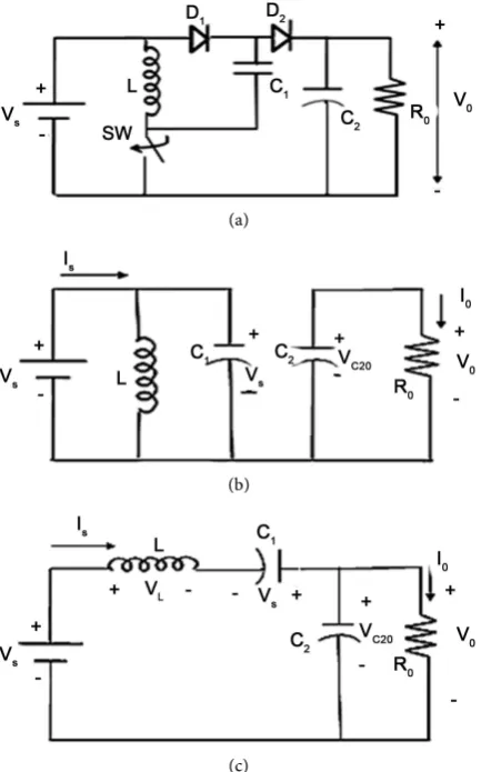
The POSLL converter shown in Figure 1(a) is the latest development in the dc–dc converters which is used to amplify the high rate of voltage transfer gain. In the given circuit diagram, the dc input voltage source is indicated as VS, SW represents the power n-channel MOSFET switch, C1 and C2 are the two capacitors, L is the inductor, D1 and D2 represent the two freewheeling diodes and Ro is the resistive load. The high power
density is achieved by operating the converter in continuous conduction mode by as-suming all the circuit parameters as ideal.
(a)
(b)
[image:4.595.265.482.72.420.2](c)
Figure 1. (a) Schematic diagram of POSLL Converter; (b) Equivalent circuit of POSLL Converter for mode1; (c) Equivalent circuit of POSLL Converter for mode 2.
Mode1 represents the ON time of the switch and mode 2 represents OFF time of the switch.
Mode 1: When the switch is in ON state, the diode D1 starts conducting and within a
very short duration of time the capacitor C1 starts charging and attains a constant
vol-tage level of source volvol-tage, VS. The current through the inductor IL depends on the
source voltage. The capacitor C2 supplies energy to the load R. The equivalent circuit
for the POSLL Converter is shown in Figure 1(b).
Mode 2: When the switch is in OFF state, the diode D2 conducts and the energy to
the capacitor C2 and the load resistance R are supplied by the decreasing inductor
cur-rent, iL. At the end of this mode, the inductor current decreases to the value of
(VO−2VS). The equivalent circuit of POSLLC for this mode of operation is shown in
Figure 1(c).
Based on the above discussion the peak–peak ripple value of the inductor current and peak peak ripple voltage of the capacitor is obtained as follows:
(
O 2 S)
L off
V V
i T
L
−
where Toff is the off time of the converter given by
(
1−α)
T, where α is the duty cycleratio and T is the total time period given by T =Ton+Toff . “∆iL” is the peak-peak value
of the inductor current. It is a regular practice to assume ∆iL as 10% to 30% of the
load current.
(
)
2 1 O C V V fRC α −∆ = (2)
where VOis the output voltage of the converter and f is the switching frequency. “∆VC”
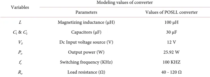
is the peak-peak ripple value of the capacitor voltage and it is assumed as 1% to 2% of the voltage across the load [10]. By using the above formulae the L and C values thus designed for the POSLL converter is illustrated in Table 1.
3. State Space Analysis of POSLL Converter
The mathematical modeling of the POSLL converter is derived based on the state space averaging technique. It is an effective method in which the PWM type converters are switched in between two or more operating states based on the duty cycle ratio of the converter. The semiconductor switch employed in the POSLL converter is turned on and off by a sequence of pulses generated at particular switching frequency, fS. Here the
inductor current iL, and capacitor voltage VC are considered as the state vectors. The
converter can be represented by the following set of dynamic equations describing the converter system during ON mode and OFF mode of the switch respectively.
During ON time,
0 d d d d L S O O i L V t V V C t R = − = (3)
During OFF time,
0 d 2 d d d L S O O S i
L V V
[image:5.595.195.553.573.704.2]t V C V t = − = = (4)
Table 1. Design parameters of POSLL converter.
Variables Modeling values of converter
Parameters Values of POSLL converter
L Magnetizing inductance (µH) 100 µH
C1 & C2 Capacitors (µF) 30 µF
VS Dc Input voltage source (V) 12 V
Po Output power (W) 25.92 W
fs Switching frequency (KHz) 100 KHZ
In general, the state modeling of the system can be represented by the following set of affine continuous time state equations,
( )
( )
( )
( )
( )
( )
1 1 2 2 , 1 , 0 S Sx t A x t B V t sw
x t A x t B V t sw
= + =
= + =
(5)
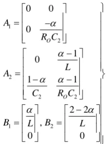
Here sw = 1 represents the on state of the switch and sw = 0 represents the off state of the switch. A1, A2, B1 and B2 are the coefficient matrices given by,
1 2 2 2 2 1 2 0 0 0 1 0 1 1 2 2 , 0 0 O O A R C L A
C R C
B L B L
α α α α α α = − − = − − − = = (6)
The output equation of the converter is represented as,
( )
[
0 1]
( )
OV t = x t . (7)
4. Design of Observer Controller for POSLL Converter
4.1. Design of State Feedback Matrix Using Pole Placement Technique
[image:6.595.316.425.177.324.2] [image:6.595.244.507.586.684.2]The ultimate objective is to design the state feedback matrix, m for the POSLL conver-ter using pole placement technique. The control scheme for the converconver-ter is shown in
Figure 2. The steady state value which has to be obtained is the controlled variable “y”. The state feedback matrices are designed in such a way that it should track any of the reference values. Here “r” is the reference value which is taken as step input. The root locus of the POSLL converter is drawn and the desired closed loop poles are placed for obtaining the desired output. The essential and adequate condition for the arbitrary pole placement of the system is that the converter system should be absolutely control-lable and it will be very much simpler to find the state feedback gain matrix when the state equations are in the controllable canonical form [1].
Pole placement method is an effectual one through which it is probable to stabilize a completely controllable system by arbitrarily choosing the closed loop poles. The as-sumptions are made that all the state variables are measurable and available for feed-back. In this method the state vector x is measured and is weighted by a constant feed-back gain matrix, m and the result is deducted from the reference signal r.
The dynamic equations corresponding to continuous time system are as follows:
(
1)
(
1)
(
) (
) (
1)
(
1)
x t+ =Ax t+ +B r−mx = A−Bm x t+ +Br t+
. (8)
The output equation is given as follows,
( ) (
) ( )
( )
y t = C−Dm x tk +Cr t . (9)
The Eigen values of (A − Bm) should be placed in the left half plane for continuous time system in controllable canonical for (A, B) pair is equivalent to (A B∨, ∨) and it is
given by,
0 1 2 1
0 1 0 0 0
0 0 1 0 0
,
1
n
A B
µ µ µ µ
∨ ∨ − = = − − − −
. (10)
It is necessary to change the converter equations into accessible canonical structure and the transformation matrix T which converts the state equation of the POSLL con-verter in to canonical form is given by the following equation,
1 2 1
2 3
1
1
1
1 0
1 0 0 0
1 0 0 0 0
n
n
n
T A AB A B
µ µ µ
µ µ µ − − − =
(11)
where µ µ1, 2,,µn are the coefficients of the characteristic equation of the system
given by,
1
1 1 0
n n
n n
s +µs− ++µ−s+µ = . (12)
The closed loop control scheme is structured by feeding back each state variable to u, thereby giving,
u= −mx (13)
where
[
1 2 n]
m= m m m . (14)
By substituting the equation (6) in equations (8) and (17), the system matrix (A −
Bm), for closed loop system is obtained and is described as,
(
0 1) (
1 2) (
2 3)
(
1)
0 1 0 0
0 0 1 0
n n
A Bm
m m m m
µ µ µ µ−
− = − + − + − + − +
Here the system equations are converted into controllable canonical form.
The characteristic equation of the closed loop system is written by inspection as fol-lows,
(
)
(
)
(
)
(
) (
)
1 2
1 2 1
1 2 0 1 0.
n n n
n n n n
sI A Bm s m s m s
m s m
µ µ
µ µ
− −
− − −
− − = + + + + +
+ + + + =
(16)
By investigating the Equations (10) and (14), it is clearly observed that the equation of the closed loop converter in controllable canonical form can be obtained by careful assessment of the open loop system equation thereby appending the suitable mi to each
and every coefficient. The required distinctive equation of the converter system for ap-propriate pole assignment is presumed as,
1 2 2
1 2 2 1 0 0
n n n
n n
s +d −s − +d − s− ++d s +d s+d = . (17)
Here di′ represents the desired coefficients. On comparison of equations (14) and
(15) it can be written as,
1, 0,1, 2, , 1
i i i
d =µ +m+ i= n− . (18)
From which,
1
i i i
m+ =d −µ. (19)
By using the above steps the values for the state feedback matrices obtained for POSLL converter is given by m=
[
62.37 59.26]
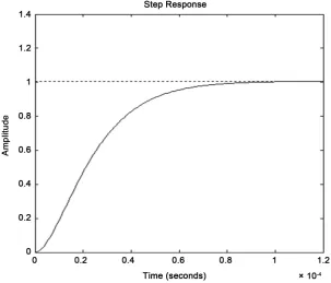
. To examine the robustness of the [image:8.595.222.526.425.684.2]control law as discussed earlier, a step input is given and the output y(t) is made to track the reference which is achieved in this case. It is illustrated in Figure 3.
4.2. Design of Full Order State Observer Gain Matrix
The full order observer gain matrix is derived using the similar pole assignment proce-dure with the eventual objective of estimating the unmeasurable state parameters. The observer always intends to act upon the error resulting in faster response of the conver-ter. The essential provision for the observer gain matrix design is that the dc-dc con-verter considered for the analysis should be completely state-controllable. Hence for the appropriate location of the observer poles the following assumptions are made as de-fined by the thumb rule.
The natural frequency of oscillation (observer controller) is approximately equal to 2 to5 times that of the natural frequency of oscillation of the system. Now, the active sys-tem equation along with a full-order state observer is described as follows:
( ) (
) ( )
1x t = A−Bm x t +Bm r. (20)
Here m1 represents the coefficient of the state feedback matrix and r represents the
step function.
The system equation along with the full order observer can be described by the fol-lowing,
( ) (
)
( )
( )
x t = A−gC x+Bu t +gy t . (21)
Here g represents the full order observer gain matrix.
Now the transfer function of the observer controller, which is a combination of state feedback matrix and full order observer, is obtained using separation principle. It is given by,
( )
( )
7 12
2 5 10
5.97 10 1.934 10
3.343 10 6.539 10
U s s
Y s s s
× + ×
=
− + × + × . (22)
5. Simulation Results and Discussion
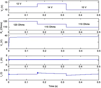
Figure 4. Output response of POSLL converter. VS—Source voltage, RO—Load resistance, VO— Output voltage, IL—Inductor current, IO—Load current.
Table 2. Performance characteristics of POSLL converter.
Sl. No. Dynamic characteristics of converter
Parameters Values
1 Settling time (s) 0.01 s
2 Rise time (s) 0.005 s
3 Peak overshoot (%) 0
4 Steady state error (V) ±0.05 V
5 Output voltage ripple (V) 0
swiftly with much lesser settling time and with no output ripples. The corresponding output current and inductor current are also given in Figure 4.
The controller performance is evaluated by changing the input voltage values from 12 V to 14 V reference values as set 36 V and to measure the output voltage, output current and inductor current are shown in Table 3. The controller confirms to be fur-ther competent in tracking the references. It is evident that the steady state error ob-served is very minimum of the order of ±0.01 V.
[image:10.595.191.555.442.559.2]pendicularly given to the controller the output voltage will be maintained constant that are shown in Table 4.
The controller performance is further evaluated by changing the reference values as 36 V and 40 V and it is exemplified in Figure 5. The controller confirms to be further competent in tracking the references. The simulation is not restricted with R load and it is also done by varying the loads as R, L and E as shown in Table 5. It is evident that the steady state error observed is very minimum of the order of ±0.03 V.
[image:11.595.204.546.253.557.2]The reference values are varied and the controller is capable of tracking any of the references as shown in Figure 5. Hence it is understood that the POSLL converter with Observer controller is proficient with faster settling time and no overshoots and un-dershoots.
Figure 5. Output response of POSLL converter with variable reference voltages. VS—Source vol-tage, RO—Load resistance, VO—Output voltage, IL—Inductor current, IO—Load current.
Table 3. Output voltage and current corresponding to line disturbances
Sl. No.
Output voltage and current value of the converter Input
voltage (V) voltage (V) Reference voltage (V) Output current (A) Output Output inductor current (A)
1 12 14 36 36 0.86 0.0586
[image:11.595.196.556.627.706.2]Table 4. Variation of output voltage corresponding to reference voltage with both line and load disturbances.
Sl. No.
Line variation
(V) Load variation (Ω) Change of reference voltage (V) Voltage across the load (V) Input voltage (V) Load resistance (Ω) Set value (V) Output voltage (V)
1 12 14 120 115 36 36.0
2 14 10 115 110 40 40.0
Table 5.Output Voltage consequent to load disturbances.
Sl. No. Load parameters Reference voltage (V) Voltage across the load (V) R (Ω) L (mH) E (V) Set value (V) Output voltage (V)
1 100 - - 36 36.00
2 110 - - 36 35.97
3 110 100e−3 - 36 36.01
4 90 50e−3 - 36 35.98
5 105 50e−3 - 36 36.00
6 100 100e−3 2 36 36.00
7 100 100e−3 4 40 40.01
6. Conclusion
Thus, the design and implementation of observer based controller for POSLL converter by means of pole assignment method and separation principle have been successfully demonstrated in MATLAB/Simulink at different operating conditions. So as to guaran-tee the robustness of the controller load estimator is derived with help of full order state feedback control. The investigation and analysis are carried out using a classical root locus method which endows with a competent and effectual compensation for the POSLL converter. The numerical examination and simulation study shows that the ob-server controller designed for POSLL converter accomplishes rigid output voltage reg-ulation, excellent dynamic characteristics and superior efficiency. It is suitable for any low power source applications such as portable electronic devices, computer peripher-als, medical equipment, and power factor correction or fuel cell applications. In future work, the POSLL converter with observer controller plus pole placement technique will be analyzed.
References
[1] Abutbuli, O., Gherlitz, A., Berkovichy, Y. and Ioinovici, A. (2003) Step-Up Switching-Mode Converter with High Voltage Gain Using a Switched-Capacitor Circuit. IEEE Transactions on Circuits and Systems, 50, 1098-1102. http://dx.doi.org/10.1109/TCSI.2003.815206 [2] Luo, F. and Ye, H. (2003) Positive Output Super Lift Converters. IEEE Transaction on
Power Electronic, 18, 105-113. http://dx.doi.org/10.1109/TPEL.2002.807198
[image:12.595.194.553.213.366.2]Fran-cis Group, London.
[4] Tseng, C. and Liang, T.J. (2004) Novel High-Efficiency Step-Up Converter. IEE Proceed-ings—Electric Power Applications, 151, 182-190.
http://dx.doi.org/10.1049/ip-epa:20040022
[5] Zhang, C.L., Wang, J.X., Li, S.H., Wu, B. and Qian, C.J. (2015) Robust Control for PWM- Based DC-DC Buck Power Converters with Uncertainty via Sampled-Data Output Feed-back. IEEE Transactions on Power Electronics, 30.
[6] Fang, L.L. and Hong, Y. (2007) Small Signal Analysis of Energy Factor and Mathematical Modeling for Power DC-DC Converters. IEEE Transactions on Power Electronics, 22, 69- 79. http://dx.doi.org/10.1109/TPEL.2006.886652
[7] Kumar, K.R. and Jeevananthan, S. (2010) A Sliding Mode Control for Positive Output Ele-mentary Luo Converter. Journal of Electrical Engineering, 10, 115-127.
[8] Chander, S., Agarwal, P. and Gupta, I. (2011) Auto-Tuned, Discrete PID Controller or DC- DC Converter for Fast Transient Response. International Conference on Power Electronics, 28-30 January 2011, 1-7. http://dx.doi.org/10.1109/iicpe.2011.5728120
[9] Shenbagalakshmi, R. and Raja, T.S.R. (2014) Discrete Prediction Controller for DC-Con- verter: Acta Scientiarum. Technology Maringá, 36, 41-48.
[10] Shenbagalakshmi, R. and Raja, T.S.R. (2013) Implementation of Robust Prediction Observ-er ControllObserv-er for DC-DC ConvObserv-ertObserv-er. Journal of Electrical Engineering & Technology, 8, 1389-1399. http://dx.doi.org/10.5370/JEET.2013.8.6.1389
[11] Lakshmi, S. and Raja, S.R. (2014) Observer-Based Controller for Current Mode Control of an Interleaved Boost Converter. Turkish Journal of Electrical Engineering & Computer Sciences.
Submit or recommend next manuscript to SCIRP and we will provide best service for you:
Accepting pre-submission inquiries through Email, Facebook, LinkedIn, Twitter, etc. A wide selection of journals (inclusive of 9 subjects, more than 200 journals)
Providing 24-hour high-quality service User-friendly online submission system Fair and swift peer-review system
Efficient typesetting and proofreading procedure
Display of the result of downloads and visits, as well as the number of cited articles Maximum dissemination of your research work
Submit your manuscript at: http://papersubmission.scirp.org/