N A N O E X P R E S S
Open Access
Properties of silicon dioxide layers with
embedded metal nanocrystals produced by
oxidation of Si:Me mixture
Andrei Novikau
1*, Peter Gaiduk
1, Ksenia Maksimova
2, Andrei Zenkevich
2Abstract
A two-dimensional layers of metal (Me) nanocrystals embedded in SiO2were produced by pulsed laser deposition of uniformly mixed Si:Me film followed by its furnace oxidation and rapid thermal annealing. The kinetics of the film oxidation and the structural properties of the prepared samples were investigated by Rutherford
backscattering spectrometry, and transmission electron microscopy, respectively. The electrical properties of the selected SiO2:Me nanocomposite films were evaluated by measuring C-VandI-V characteristics on a metal-oxide-semiconductor stack. It is found that Me segregation induced by Si:Me mixture oxidation results in the formation of a high density of Me and silicide nanocrystals in thin film SiO2 matrix. Strong evidence of oxidation temperature as well as impurity type effect on the charge storage in crystalline Me-nanodot layer is demonstrated by the hysteresis behavior of the high-frequencyC-Vcurves.
Introduction
During the last decade, much attention has been focused on the investigation of semiconductor and metallic nanocrystals (NCs) or nanoclusters embedded in dielec-tric madielec-trices. The interest is motivated by possible applications of such nanocomposite structures. Particu-larly, semiconductor or metal NCs embedded in SiO2 dielectric layer of a metal-oxide-semiconductor field-effect transistor may replace SiNx floating gate in con-ventional Flash memory devices, allowing for thinner injection oxides, and subsequently, smaller operating voltages, longer retention time, and faster write/erase speeds [1-3]. The performance of such memory struc-ture strongly depends on the characteristics of the NCs arrays, such as their size, shape, spatial distribution, electronic band alignment.
Several approaches have been recently tested for the formation of NCs in dielectric layers. Among those, self-assembling of NCs in dielectric layers fabricated by the low-energy ion implantation and different deposition techniques has been studied by several groups [4-7]. A strong memory effect in MOS devices using oxides with
Si or Ge NCs was reported in [4,6]. However, the implantation of Ge at the silicon-tunnel oxide interface creates trap sites and results in the degradation of the device performance [4]. The growth technique using MBE deposition of 0.7-1 nm thick Ge layer followed by rapid thermal processing was implemented in [8,9]. An alternative method for Ge NCs production [10] consists of the following steps: low pressure chemical vapor deposition of thin Si-Ge layer, thermal wet or dry oxida-tion, and thermal treatment in an inert ambient (reduc-tion). Recently, a method to form an ultrathin nanocomposite SiO2:NC-Me layers at room temperature by combining the deposition of Si:Me mixed layer on the pre-oxidized Si substrate and its further oxidation in the glow discharge oxygen plasma was proposed [11].
In this article, a similar approach was used to produce thin SiO2 layers with an embedded layer of metal NCs. Au and Pt were chosen as metal components in Si:Me mixtures since both metals are believed to catalyze Si oxidation thus reducing the processing temperature, while neither Au nor Pt form stable oxides. Both Pt and Au embedded as NCs in dielectric matrix are attractive materials in plasmonics [12]. In addition, both metals have much higher electron work functions compared to semiconductors, particularly, Ge, and it is interesting to investigate the effect of the NC work function on the
* Correspondence: [email protected]
1Belarusian State University, 4 prosp. Nezavisimosti, 220030, Minsk, Belarus
Full list of author information is available at the end of the article
electrical properties of the MOS stack with embedded NCs. As the first step, a thin Si:Me layer with the pre-cisely pre-defined composition was grown by pulsed laser deposition (PLD) technique. The oxidation of Si: Me mixture was expected to result in the segregation of the noble metal in NCs distributed in the SiO2 matrix. By means of analyzing the Si(Ox):Me elemental depth distributions as a function of the annealing temperature and/or time, we attempted to investigate the kinetics of the composite structure formation. This information was supplemented by microstructural transmission elec-tron microscopy (TEM) analysis and further–by electri-cal measurements on metal/SiO2:Me-NC/Si capacitors.
Experimental
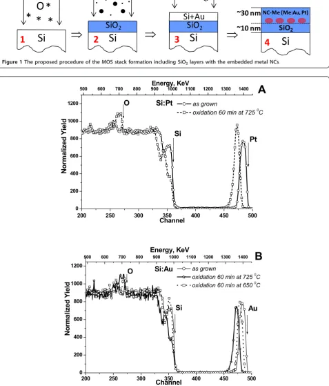
N-type Si(001) wafers were used as substrates. The uni-form SiO2 layer 6 nm in thickness (tunnel oxide) was first grown in a dry oxygen ambiance. An amorphous Si: Me (Me = Au, Pt) layer 20 nm in thickness was then deposited by PLD at room temperature. The computer-ized ultra-high vacuum (base pressure P = 10-6 Pa) home-made PLD setup employing YAG:Nd laser (l= 1,064μm) and operating in the Q-switched regime (τ= 15 ns) at the variable output energies E = 50-200 mJ and the repetition ratesν = 5-50 Hz was employed to ablate from the elemental Si and Me (Me = Au, Pt) tar-gets. The pre-calculated composition of the Si:Me mix-ture necessary to form the desired nanocomposite structure was provided by choosing the exact ratio of Si vs. Me deposition pulses in a deposition cycle during the Si:Me layer growth. The sandwiched Si:Me/SiO2/Si samples were further thermally oxidized in dry oxygen ambient. To exclude the coalescence of the segregating metal NCs, the thermal budget should be minimized. Therefore, to determine the minimal temperatures to oxidize Si:Me mixtures at our conditions, the prelimin-ary experiments were performed. It is worth noting that the presence of a noble metal in Si:Me mixture is found to significantly reduce the oxidation temperatures as compared to pure Si. Thus, the chosen oxidation condi-tions wereT = 640-725°C for 60-540 min. Finally, the thermally oxidized structures were subjected to rapid thermal annealing in dry nitrogen ambient atT= 900°C for 30 s. The sequential processing steps are shown in Figure 1. A reference SiO2/Si sample with no metal NCs was prepared for comparison.
The composition of and the metal depth distribution in the samples were measured using Rutherford back-scattering spectrometry (RBS) with a He+
beam at E= 1.5 MeV. The spectra were taken simultaneously at two different scattering angles,θ= 10° andθ= 75°, with the former geometry being used to calculate the integral metal concentration in Si:Me, while the latter one to observe possible changes in the metal distribution upon
oxidation. The experimental spectra were analyzed using the RUMP software [13]. The structural quality and the phase composition were analyzed using the TEM in both plain-view and cross-sectional geometries using a Philips CM20 instrument operating at U = 200 kV. MOS capacitors with In electrodes were fabricated, and the high-frequencyC-Vmeasurements were carried out using a serial HP4156B instrument.
Results and discussion
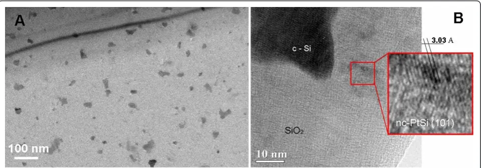
The typical RBS spectra from the as-grown and ther-mally treated Si:Me/SiO2/Si samples are presented in Figure 2. The RBS spectra show that the thickness of as-deposited Si:Au layers is about 20 nm. The metal concentration in the deposited layers is in the range 2.5-4.5%. The shift of both Au and Pt peaks to the lower energies upon thermal oxidation evidencing the pile up of metal atoms at the SiO2/Si interface is clearly observed in RBS spectra. The observed evolution of Pt and Au concentration profiles indicates the complete rejection of Me atoms from the oxide during thermal oxidation of a-Si:Me layer. The detailed analysis of RBS data (Figure 2) reveals that Au and Pt segregation depends on the oxidation conditions. In particular, neither evaporation nor diffusion of Au or Pt in SiO2 layer takes place during thermal oxidation in dry O2. On the contrary, oxidation at higher temperatures results in a strong loss (about 30%) of Me from the SiO2layer, apparently due to evaporation and partial dif-fusion into the Si substrate.
Si
*
*
*
*
*
*
*
O
1
SiO
2.
.
.
.
.
• •
•
Si+Au
.
.
Si
2
SiO
2
Si+Au
*
*
*
*
*
*
O
Si
3
SiO
2Si
~30 nm
~10 nm
NC-Me (Me:Au, Pt)
[image:3.595.60.538.134.694.2]4
Figure 1The proposed procedure of the MOS stack formation including SiO2layers with the embedded metal NCs.
200 250 300 350 400 450 500
0 200 400 600 800 1000 1200
500 600 700 800 900Energy, KeV1000 1100 1200 1300 1400
Pt
Si
O
A
Si:Pt
as grownoxidation 60 min at 7250C
N
o
rm
aliz
ed
Y
ie
ld
Channel
200 250 300 350 400 450 500
0 200 400 600 800 1000 1200
500 600 700 800 900 1000 1100 1200 1300 1400
Energy, KeV
B
Si:Au as grown
oxidation 60 min at 725 0C
oxidation 60 min at 650 0C
No
rm
al
iz
ed Yi
el
d
Channel O
Si Au
Figure 2RBS spectra from as grown and thermally oxidized Si:Me/SiO2/Si samples:(a)RBS spectra (E= 1.5 MeV,θ= 75°) from Si:Pt/SiO2/Si
samples thermally oxidized atT= 725°C for 60 min in O2followed by thermal annealing in N2atT= 900°C for 30 s. as compared with as-grown
indicated the formation of a metastable Au silicide dur-ing the room temperature deposition and its further decomposition to metallic Au upon oxidation.
The self-assembling phenomenon of the formation of metal and silicide NCs in SiO2 can be explained using two mechanisms. A solubility of impurities in SiO2 is quite low, and therefore the structures obtained after metal segregation and piling up between two SiO2layers (tunnel oxide and SiO2 capping layer) were transformed into the supersaturated solution. It is well known that under the thermal treatment the decomposition of supersaturated solution takes place eventually resulting in the phase separation and the formation of the metal NCs in a dielectric (oxide) matrix. On the next stage, the Ostwald ripening of the formed NCs occurs. This implies the diffusion of metal atoms from the valley regions of the islands toward their respective centers forming spherical nanocrystals to achieve greater volume-to-surface ratio. In our model, the initial NCs are formed during the oxidation of the Si:Me layer. After the oxidation is completed, the sample is still kept at elevated temperature facilitating the coalescence of Me NCs.
The effect of the oxidation temperature as well as the type of the embedded Me on the efficiency of the charge storage was studied by the high-frequencyC-V measure-ments. The hysteresis inC-Vcurves was found different for the structures containing Au and PtSi NCs (Figure 4). The maximal value of the flat-band voltage shiftU= 1.8 V for theVgsweep -5/+3 V was obtained for SiO2:NC-Au based structures prepared by dry oxidation. On the contrary, in the case of SiO2:NC-PtSi, the maximal flat-band voltage shift was U = 1.2 V. By increasing Vg sweep up to 5 V, a gradual increase of the flat-band vol-tage shift was achieved. Since high positive gate volvol-tages
shift C-Vcurves in the direction of the stored negative charges, it is concluded that the charge trapping occurs through the electron injection from the substrate into the oxide. No flat-band voltage shift was observed for the reference sample prepared with pure SiO2, oxidized atT = 850°C for 60 min in O2 ambient. It is therefore concluded that the effect of charge storage is related to the NCs.
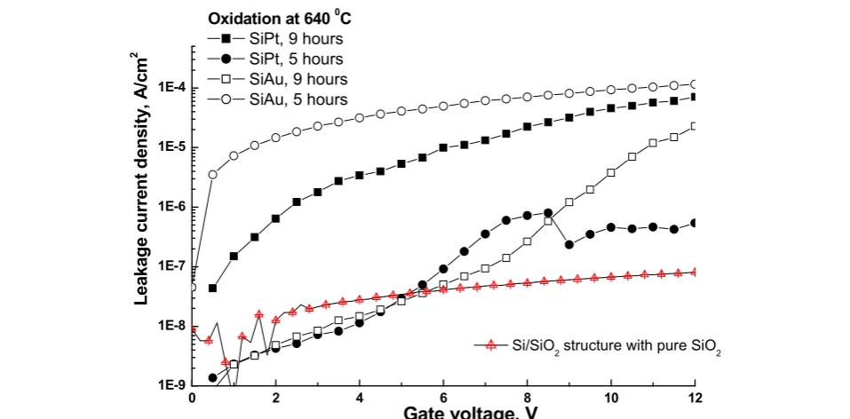
One of the major reasons for the loss of charge in the floating gate structures is the leakage current. The mea-suredI-Vcurves (Figure 5) from Si:Au and Si:Pt samples oxidized in dry ambient reveal that the leakage current density can be reduced down to 10-8 A/cm2. The low leakage currents achieved are explained by the high quality of both tunneling and capping oxide formed by dry thermal process compared with the deposited oxides used in the alternative methods of MOS capacitor for-mation [15]. It is found that the oxidation temperature has also a strong effect on the leakage current, and therefore the oxidation conditions should be optimized for each type of embedded metal NCs.
Conclusion
[image:4.595.59.539.89.257.2]In this study, the authors have demonstrated the growth of thin SiO2layers with embedded metal and metal sili-cide NCs by the combination of Si:Me mixture by PLD at room temperature and its thermal oxidation. By means of this fabrication technique, it is possible to produce a sheet of crystalline metal nanocrystals at any desirable depth in the oxide. The metal segregation process during thermal oxidation results in the formation of a high areal density of crystalline Au and PtSi dots 10-20 nm in dia-meter which are distributed in the silicon dioxide at a distance of 5-6 nm from the crystalline Si substrate. The charge storage effect is evident fromC-Vcharacteristics
on MOS capacitors, and the results indicate the injection of the electrons from the substrate. The flat-band voltage shift of about 1.2-1.8 V for Vg sweeps of -5/+3 V is achieved. It is shown that the leakage current density depends mostly upon the oxidation conditions, and for
both types of metal NCs (Au and PtSi), it was measured to be around 10-8A/cm2. The reproducibility and the precision of the proposed fabrication technique (PLD and thermal treatment) to produce a 2 D array of well-separated nanocrystals in a SiO2layer suggest that this
-5 -4 -3 -2 -1 0 1 2 3 4
6 8 10 12 14 16 18 20
-5 -4 -3 -2 -1 0 1 2 3 4
6 8 10 12 14 16 18 20 22 24 26 28 30
SiPt
oxidation 9 h, 640 0ɋ oxidation 5 h, 640 0ɋ
C
Si O2, p
F
Gate voltage, V
SiAu
oxidation 9 h, 640 0C
[image:5.595.57.538.88.347.2]oxidation 5 h, 640 0C
Figure 4High-frequency C-Vcurves measured from Si:Au and Si:Pt samples, oxidized atT= 640°C for 5 and 9 h in dry O2,
respectively. A gate voltage sweep from inversion to accumulation and from accumulation to inversion is shown on the figure by arrows.
0 2 4 6 8 10 12
1E-9 1E-8 1E-7 1E-6 1E-5 1E-4
Si/SiO2 structure with pure SiO2
Oxidation at 640 0
C SiPt, 9 hours SiPt, 5 hours SiAu, 9 hours SiAu, 5 hours
Le
ak
ag
e cu
rr
en
t
d
en
si
ty
,
Ⱥ
/
ɫ
m
2
Gate voltage, V
Figure 5Leakage current vs. gate voltage characteristics obtained from the oxidized Si:Au and Si:Pt samples atT= 640°C. TheI-V
[image:5.595.58.537.463.699.2]method can be applied for the fabrication of functional MOS structures.
Abbreviations
NCs: nanocrystals; PLD: pulsed laser deposition; RBS: Rutherford backscattering spectrometry; TEM: transmission electron microscopy; MOS: metal-oxide-semiconductor.
Acknowledgements
We would like to acknowledge the help received from A. Orekhov (Institute of Crystallography, RAS) for high resolution TEM analysis.
This study is a part of the Belarusian Scientific Research Program
“Electronics”and was funded also by the Belorussian and Russian Foundations for Fundamental Research (projects T08P-184/90023).
Author details
1Belarusian State University, 4 prosp. Nezavisimosti, 220030, Minsk, Belarus 2NRNU“Moscow Engineering Physics Institute”, 31 Kashirskoe shausse,
115409, Moscow, Russian Federation
Authors’contributions
AN participated in the RBS analysis and carried out the electrical characterization, participated in the design of the study and drafted the manuscript. KM carried out the pulsed laser deposition and experimental data analysis. PG conceived of the study, and participated in its design and coordination. AZ participated in the design of the study, coordinated TEM analysis and significantly contributed to the writing of manuscript. All authors read and approved the final manuscript.
Competing interests
The authors declare that they have no competing interests.
Received: 21 September 2010 Accepted: 16 February 2011 Published: 16 February 2011
References
1. Kwon YH, Park CJ, Lee WC, Fu DJ, Shon Y, Kang TW, Hong CY, Cho HY, Wang KL:Memory effects related to deep levels in metal-oxide-semiconductor structure with nanocristalline Si.Appl Phys Lett2002,
80:2502.
2. Tiwari S, Rana F, Hanafi H, Hartstein A, Crabbe EF, Chan K:A silicon nanocrystals based memory.Appl Phys Lett1996,68:1377.
3. Tiwari S, Rana F, Chan K, Shi L, Hanafi H:Single charge and confinement effect in nanocrystal memories.Appl Phys Lett1996,69:1232.
4. Normand P, Kapetanakis E, Dimitrakis P, Tsoukalas D, Beltsios K, Cherkasin N, Bonafos C, Benassayag G, Coffin H, Claverie A, Soncini V, Agarwai A, Ameen A:Effect of annealing enviroment on the memory properties of thin oxides with embedded Si nanocrystals obtained by low-energy ion-beam synthesis.Appl Phys Lett2003,83:168.
5. Beyer V, von Borany J:Elemental redistribution and Ge loss during ion-beam synthesis of Ge nanocrystals in SiO2 films.Phys Rev B2008,
77:014107.
6. Baron T, Pelissier B, Perniola L, Mazen F, Hartman JM, Rolland G:Chemical vapor deposition of Ge nanocrystals on SiO2.Appl Phys Lett2003,
83:1444.
7. Choi WK, Chim WK, Heng CL, Teo LW, Ho V, Ng V, Antoniadis DA, Fitzgerald EA:Observation of memory effect in Germanium nanocrystals enbedded in an amorphous silicon oxide matrix of a metal-oxide-semiconductor structure.Appl Phys Lett2002,80:2014.
8. Kanjilal A, Hansen JL, Gaiduk P, Larsen AN, Cherkashin N, Claverie A, Normand P, Kapelanakis E, Skaratos D, Tsoukalas D:Structural and electrical properties of silicon dioxide layers with embedded Germanium nanocrystals grown by molecular beam epitaxy.Appl Phys Lett2003,
82:1212.
9. Kanjilal A, Hansen JL, Gaiduk P, Larsen AN, Normand P, Dimitrakis P, Tsoukalas D, Cherkashin N, Claverie A:Size and aerial density distributions of Ge nanocrystals in a SiO2 layer produced by molecular beam epitaxy and rapid thermal processing.Appl Phys A2005,81:363.
10. Novikau AG, Gaiduk PI, Pshenichnij EN, Nalivaijko OYu, Malishev VS, Plebanovich VI:Nanocrystal floating gate produced by CVD and thermal processing.Proceedings of the ICMNE, Moscow, Zvenigorod, Russia2007,
0000:O3-O2.
11. Zenkevich AV, Lebedinskii YuYu, Timofeyev AA, Isayev IA, Tronin VN:
Formation of ultrathin nanocomposite SiO2:nc-Au structure by pulsed laser deposition.Appl Surf Sci2009,255:5355.
12. Atwater HA, Polman A:Plasmonics for improved photovoltaic devices. Nat Mater2010,9:205.
13. Computer Graphic Service.[http://www.genplot.com].
14. Maksimova K, Matveev Yu, Zenkevich A, Nevolin V, Novikov A, Gaiduk P, Orekhov A:Investigation of nanocomposite SiO2:Me structures, formed by metal segregation during thermal oxidation of Si:Me alloy layers. Perspektivnye Materialy2010,2:33, (in Russian).
15. Tan Z, Samanta SK, Yoo WJ, Lee S:Self-assembly of Ni nanocrystals on HfO2 and N-assisted Ni confinement for nonvolatile memory application.Appl Phys Lett2005,86:013107.
doi:10.1186/1556-276X-6-148
Cite this article as:Novikauet al.:Properties of silicon dioxide layers with embedded metal nanocrystals produced by oxidation of Si:Me
mixture.Nanoscale Research Letters20116:148.
Submit your manuscript to a
journal and benefi t from:
7Convenient online submission
7Rigorous peer review
7Immediate publication on acceptance
7Open access: articles freely available online
7High visibility within the fi eld
7Retaining the copyright to your article