N A N O E X P R E S S
Open Access
Comparative Analysis of Defects in
Mg-Implanted and Mg-Doped GaN Layers on
Freestanding GaN Substrates
Ashutosh Kumar
1*, Kazutaka Mitsuishi
1*, Toru Hara
1, Koji Kimoto
1, Yoshihiro Irokawa
1, Toshihide Nabatame
1,
Shinya Takashima
2, Katsunori Ueno
2, Masaharu Edo
2and Yasuo Koide
1Abstract
Inefficient Mg-induced p-type doping has been remained a major obstacle in the development of GaN-based electronic devices for solid-state lighting and power applications. This study reports comparative structural analysis of defects in GaN layers on freestanding GaN substrates where Mg incorporation is carried out via two approaches: ion implantation and epitaxial doping. Scanning transmission electron microscopy revealed the existence of pyramidal and line defects only in Mg-implanted sample whereas Mg-doped sample did not show presence of these defects which suggests that nature of defects depends upon incorporation method. From secondary ion mass spectrometry, a direct correspondence is observed between Mg concentrations and location and type of these defects. Our investigations suggest that these pyramidal and line defects are Mg-rich species and their formation may lead to reduced free hole densities which is still a major concern for p-GaN-based material and devices. As freestanding GaN substrates offer a platform for realization of p-n junction-based vertical devices, comparative structural investigation of defects originated due to different Mg incorporation processes in GaN layers on such substrates is likely to give more insight towards understanding Mg self-compensation mechanisms and then optimizing Mg doping and/or implantation process for the advancement of GaN-based device technology.
Keywords:GaN, STEM, SIMS, Pyramidal defects, Line defects
Introduction
Over the last three decades, GaN has emerged as one of the most investigated compound semiconductors all across the world. This is mainly due to its tremendous po-tential not only in solid-state lighting applications but also in high-power, high-frequency, and high-temperature op-erations [1–8]. For successful employment of devices based on GaN and related heterostructures into such ap-plications and operations, controllable n-type and p-type doping is the key requirement. In this aspect, achieving and controlling n-type doping in GaN epilayers or single crystals are now optimized to a great extent in comparison to its p-type counterpart which is still a bottleneck for the academia as well as industry. Till now, Mg has proven to be the most efficient p-type dopant despite of its high
activation energy which requires a large amount of Mg concentrations (around 1019cm−3or more) to be incorpo-rated in order to achieve reasonable free hole concentra-tions close to 1018cm−3. Any increase in Mg atomic concentrations beyond 1019cm−3lead to a decrease in the free hole concentration [9–11]. This phenomenon is mainly attributed to the creation of N vacancies [12–14], Mg-related point defects [10,15], or Mg vacancies-related charged and/or neutral complexes which lowers the Fermi level and saturates free hole concentrations [16, 17]. On the basis of photoluminescence measurements giving rise to a peak at 2.9 eV, a deep donor defect complex Mg-VN was also believed to be the one of the primary reason for the self-compensation mechanism. [17–19]. Hence, des-pite of the number of significant research attempts made towards understanding the Mg incorporation in GaN, this problem remains still unclear and further analysis needs to be carried out.
* Correspondence:[email protected];
1National Institute for Materials Science, Tsukuba, Ibaraki 305-0047, Japan Full list of author information is available at the end of the article
Most of the earlier reports on defects analysis using atomic scale microscopic studies are based on Mg-doped GaN layers grown on sapphire using metal organic chem-ical vapor deposition (MOCVD) or molecular beam epi-taxy (MBE). To the best of our knowledge, there are only few reports on defects analysis in Mg-doped freestanding GaN substrates and there is no report on transmission electron microscopy-based defects analysis in free-standing GaN substrates where Mg is incorporated via ion-implantation. It is now well accepted that free-standing GaN substrates have several advantages over MOCVD/MBE grown GaN layers on foreign substrates due to reduced level of dislocation densities and their applications in efficient vertical devices. Achieving suf-ficient p-type dopants activity in such substrates via ion-implantation needs to be explored for commer-cialization and development of GaN-based solid-state lighting and high-power devices. Keeping all these is-sues as primary objective, we have carried out detailed structural analysis of Mg-incorporated defects in GaN freestanding layers where Mg incorporation is achieved by doping as well as ion implantation.
Experimental Methods
Freestanding n-GaN substrates grown using hydride vapor phase epitaxy are used in our study. Thereafter, epitaxial layers are grown by MOCVD on these sub-strates. Mg incorporation is carried out via two ap-proaches: ion implantation and epitaxial doping. In the first case, Mg is implanted into 4-μm-thick undoped GaN epitaxial layer without depositing any protection layer on undoped GaN layers, while in the second case, 1-μm-thick Mg-doped GaN is epitaxially grown on 4-μm-thick undoped GaN layers continuously. For a reli-able comparison, level of Mg incorporation is kept same as 4 × 1019cm−3in both cases. The Mg implantation is carried out at 500 °C followed by annealing at 1350 °C
for dopants’ activation. The implantation energies are taken as 15, 30, 55, 95, and 180 keV with respective dos-ages of 3.0 × 10¹³, 5.5 × 10¹⁵, 1.1 × 10¹⁴, 1.9 × 10¹⁴, and 8 × 1014cm−2, to obtain a 200-nm-deep box profile. Hall measurements are carried out to evaluate the electrical properties of both Mg-doped and Mg-implanted GaN sam-ples. For Mg-doped GaN sample, hole concentration and mobility are found to be 3.4 × 1017cm−3and 9.5 cm2/V-s. On the other hand, electrical properties of Mg-implanted sample could not be evaluated properly due to its highly resistive nature. The distribution of Mg as a function of depth is investigated using secondary ion mass spectrometry (SIMS) while scanning transmission electron microscopy (STEM) analysis is used for struc-tural investigations of Mg-induced defects. For this, STEM and electron energy dispersive X-ray spectros-copy (EDS) have been carried out by JEOL JEM-ARM200F operated at 200 and 80 kV. For these studies, TEM specimens were prepared by focused ion-beam milling using Ga beams followed by a liquid nitrogen-cooled low-energy Ar ion milling.
Results and Discussion
Defects Analysis in Mg-Implanted GaN Layer
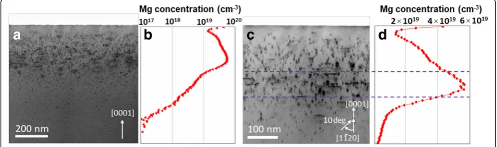
Figure 1(a) shows the bright field (BF)-STEM image of Mg-implanted GaN whereas (b) shows the correspond-ing SIMS profile. The arrow shown in Fig. 1(a) repre-sents positive [0001] direction, and images are viewed along [11 2 0] zone axis. It can be seen that defects are not uniformly distributed as a function of depth, in fact, a direct correlation is seen between the concentrations of Mg and defects. Most of the defects are accumulated at about 150 nm from the surface where Mg concentra-tion is more than 1019cm−3 as observed from SIMS measurements. For better understanding of defects and their visualizations due to Mg implantation in GaN,
[image:2.595.56.540.541.684.2]imaging is carried out in off-zone axis condition by tilt-ing the sample 10° around c-axis from [1120] axis. This condition weakens the diffraction contrast due to perfect crystal and enhances the defects contrast which allows better visualization of the defects in comparison to sur-rounding environment. BF-STEM image of Mg-implanted GaN sample taken under this off-zone axis conditions is shown in Fig. 1(c) where some line defects are seen at a depth of about 200 nm from the surface. The correspond-ing Mg SIMS profile is presented in (d) in linear scale where a direct correspondence is observed between the existence of these line defects and Mg concentration. These defects are found to be located in a narrow region where Mg concentration is about mid 1019cm−3range.
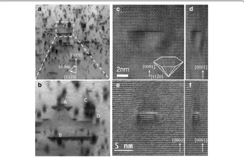
Further, high-magnification BF-STEM imaging is carried out under off-zone axis condition as shown in Fig. 2(a) with (b) showing the selected region of (a) at a higher magnification. As shown in (b), four kinds of structures la-belled as A, B, C, and D are observed. The defects lala-belled as“A”are of pyramidal shape whereas “B”appear as line defects.
The structural observations of these defects are im-portant from view point of understanding Mg compen-sation mechanisms, and next sections of the manuscript are mainly devoted to structural analysis of type“A”and
“B” defects. The structures shown as “A” are pyramidal defects with positive [0001] direction pointing towards their head, their base on [0001] plane with six walls on [1123] planes inclined as shown by high-resolution TEM image of one such defect in Fig.2(c). The schematic rep-resentation of such pyramidal domain is also shown in Fig.2(c). Figure2(c) is squeezed perpendicular to [0001] direction as shown in (d) where lattice appears to be distorted in pyramidal domain in comparison to sur-rounding GaN matrix, indicating displacement between the Ga and N sublattices inside and outside of these pyramidal domains. This is consistent with the findings of the Vennegues et al. [20] where similar type of pyr-amidal domains are observed. The similar pyrpyr-amidal shape defects are earlier observed in Mg-doped GaN films and their existence is usually explained by modification in GaN atomic structure due to Mg introduction [19–24].
[image:3.595.59.538.367.674.2]Liliental-Weber et al. [25,26] proposed that such pyram-idal defects originate from Mg-rich clusters present near the head of these pyramids. The GaN structure in wurtzite phase is usually described by hexagonal stacking of N planes with half of the N sublattice tetrahedra sites filled by Ga atoms. Vennegues et al. [27] on the basis of their in-vestigations proposed that introducing higher level of Mg in GaN results in the substitution of Ga by Mg, forming Mg3N2, a Mg-N compound reported to have antibixbyite structure. The antibixbyte structure of Mg3N2 corre-sponds to the filling of N sublattice tetrahedra sites by Mg which occupies three out of every four sites. As per the model proposed by Vennegues et al. [27], a pyramidal do-main can be considered as two GaN crystals of opposite polarity separated by a monolayer of Mg3N2. This is fur-ther supported by the investigations of Hansen et al. [28] where these pyramidal domains were proposed to be Mg3N2inclusions. Vennegues et al. [27] and Leroux et al. [23] also reported that formation of such pyramidal do-mains having nanometer size also requires a Mg incorpor-ation of low to mid 1019cm−3 range. This is consistent with our findings where the pyramidal shape defects are observed at lower to mid-1019cm−3Mg concentrations as seen from the correlation between STEM image (Fig.1(c)) and corresponding SIMS profile (Fig.1(d)). Therefore, the pyramidal shape defects labelled as structures“A”in Fig.2 (b) of our study are believed to be Mg-rich pyramidal do-mains and their formation can be directly linked to the Mg compensation mechanism in p-GaN layers. Other types of defects as shown in Fig.2(b) are type“C”and“D” defects which are essentially similar structures with vari-ation in their dimensions. The contrast which appears to be elongated along the [0001] direction when viewed from [11 2 0] axis, is likely to be strain originated. For further clarifying this, high-resolution TEM image of one such
similar defect is presented in Fig.2(e) with (f) showing the same image squeezed perpendicular to [0001] direction. The distorted lattice along [0001] direction suggests differ-ent lattice constant due to differdiffer-ent strain field along this direction. As Mg is smaller in size in comparison to Ga, its incorporation on the Ga sites is expected to produce strain in the lattice which may lead to this contrast around these defects.
Another type of defects, labeled as“B”in Fig. 2(b) ap-pear to be line defects perpendicular to [0001] direction, when viewed from [1120] axis. It is important to note that such type of defects appear to be accumulated in a narrow region having higher Mg concentrations (as observed from correspondence between BF-STEM image and Mg SIMS profile shown in Fig.1(c) and (d)) which suggests that their formation is associated with the over-incorporation of Mg. Another observation is the presence of the pyramidal do-mains on the edges of these line defects which indicate that accumulation of these domains may result in their forma-tion. However, one should not rule out that it could simply be a random overlap of pyramidal and line defects and further investigations are needed in this direction. The BF-STEM image showing these types of defects is pre-sented in Fig. 3(a). For better understanding of these defects, sample is tilted at about 10° around the axis per-pendicular to [0001] direction and obtained BF-STEM image is shown in Fig. 3(b). This tilting of the sample strongly excites the diffraction spots along 1–100 direction, which results in enhanced contrast from the strain field in the direction surrounding the defect. From this strain field contrast, the defect which appeared as the line (see Fig.2(a) and (b)) actually consists of a pair of lines separated by few nm, deeper in [0001] direction.
There could be a possibility of presence of Mg in these defects as they appear in the narrower region where Mg
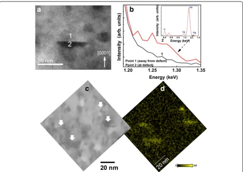
[image:4.595.57.539.521.695.2]concentration is higher than 1019cm−3as observed from the correspondence between STEM image (Fig. 1(c)) and Mg SIMS profile (Fig.1(d)). To validate this belief of these types of defects having Mg, we carried out scanning transmission electron microscopy-energy-dispersive spec-troscopy (STEM-EDS) measurements with EDS probe diameter less than 0.2 nm, at two different regions:
“away from defect” and“at defect” labelled as points 1 and 2 respectively as shown in Fig. 4(a). The compara-tive EDS spectra from points 1 and 2 in the energy range of 1.19 keV to 1.35 keV where Mg peak is ex-pected are plotted in Fig. 4(b) with inset showing full EDS spectra. The presence of Mg is clearly seen at de-fect (point 2). To further justify this, we have carried out STEM-EDS mapping on a similar Mg-implanted GaN sample. Figure 4 (c) presents STEM image of Mg-implanted GaN sample with downward arrows showing these line defects, and the corresponding EDS map of Mg is shown in Fig. 4 (d). The presence of Mg
is clearly seen in these defects. Therefore, these defects contain Mg and their formation at Mg concentrations higher than 1019cm−3 is likely to be another cause of Mg compensation.
Defects Analysis in Mg-Doped GaN Layer
Next, we have carried out structural investigations on the GaN sample where 1-μm thick Mg-doped GaN layer is epitaxially grown on 4-μm-thick undoped GaN epitaxial layer. It is worth mentioning again that the level of Mg is kept same, i.e., 4 × 1019cm−3for a meaningful comparison between two approaches of Mg incorporation: epitaxially doped and ion implantation. Figure5(a) shows BF-STEM image of Mg-doped GaN grown epitaxially on freestand-ing GaN substrates, viewed along [11 2 0] whereas (b) shows Mg profile as a function of GaN depth obtained using SIMS. Note that Mg concentration remains almost constant at about 4 × 1019cm−3within the field of view of
[image:5.595.58.539.342.682.2]Fig.5(a) (up to 700 nm) unlike the earlier case of Mg-im-planted GaN where Mg concentration was found to be a function of GaN depth (see Figs.1(a)–(d)).
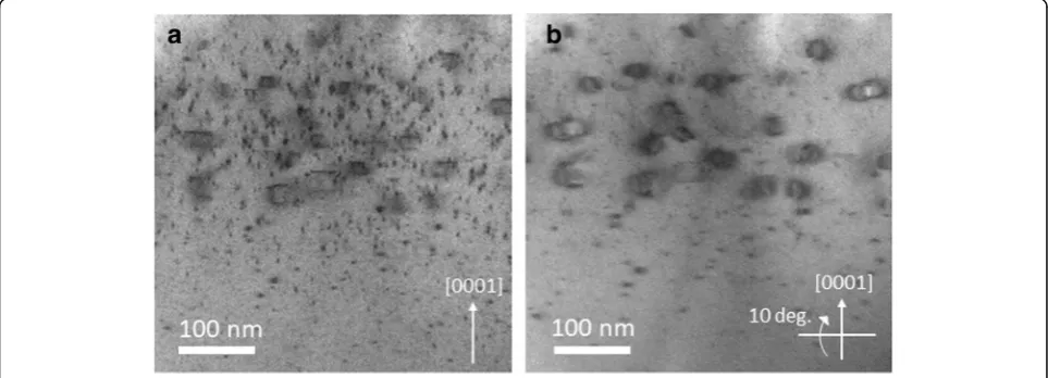
To carry out defects analysis in Mg-doped GaN sam-ple, STEM imaging in off-zone axis condition by tilting the sample at 10° around c-axis from [1120] axis is car-ried out. Figures 6 (a) and (b) represents the BF-STEM and DF-STEM images where dot like defects having size of about 5 nm are observed to be uniformly distributed across the sample. Note here that Mg profile also ap-pears to be uniform in this case as observed from SIMS profile (see Fig. 5(b)). The uniform distribution of Mg and these defects across the GaN sample suggests a dir-ect correlation between these defdir-ects and Mg incorpor-ation. These dot like defects of about 5 nm are likely to be precipitates of Mg (and possibly induced stacking faults by it). Due to their small size, Mg precipitation
itself could not be directly confirmed by EDS measure-ments (Ga and Mg peaks lie quite close to each other which makes mapping of small concentration difference extremely difficult).
This observation is completely different from the earlier case of Mg-implanted sample where defects are found to be accumulated at 200 nm from the surface where Mg concentration was maximum. In addition, unlike the Mg-implanted sample, we did not observe any pyramidal and two-line defects, (labelled as A and B in Fig. 2(b)) in Mg-doped GaN sample. Interestingly pyramidal and line defects are also reported in the GaN samples where Mg is incorporated by techniques other than ion-implantation. For example, Khromov et al. [29] reported the existence of pyramidal defects in Mg-doped GaN samples grown by MOCVD. However, they observed such defects only in higher doped GaN
Fig. 5aCross sectional bright field STEM image of Mg-doped bulk GaN sample obtained along [1120] axis and̅ bcorresponding depth profile of Mg obtained using SIMS. Dot-like defects are found to be uniformly distributed across the sample
[image:6.595.60.539.88.271.2] [image:6.595.58.539.556.702.2]sample where Mg concentration was about ~ 5 × 1019cm−3. However, in samples with Mg ~ 2 × 1018cm−3, these pyr-amidal domains were not observed. Vennegues et al. [27] also observed such pyramidal domains in MOCVD grown Mg-doped GaN samples with Mg concentrations lying in the mid 1019cm−3range. They did not observe such defects in sample with Mg concentrations lower than 1019cm−3. In our work, similar level of Mg ~ 4 × 1019cm−3 is incorpo-rated via ion-implantation and epitaxial doping to analyze the presence of these defects. These defects are only ob-served in Mg-implanted sample, not in Mg-doped sample which suggests that Mg distribution should also be con-sidered for explaining their existence. From SIMS mea-surements, Mg is found to be non-uniformly distributed in the Mg-implanted sample (Figs. 1(b) and (d)) whereas Mg-doped sample showed uniform distribution of Mg (Fig.5(b)). Moreover, in Mg-implanted sample, these de-fects were found to be existing only in a narrow window with higher Mg concentration in comparison to surround-ing matrix. Therefore, formation of these defects is linked with the level of incorporated Mg and distribu-tion of Mg and they are likely to be form in the regions where Mg lies in the range of 1019cm−3. It appears that non-uniform Mg profile in Mg-implanted sample leads to a non-uniform distribution of defects. However, one should not deny the possibilities like non-uniformly distributed defects causing non-uniform Mg distribu-tion or dependency of Mg implantadistribu-tion profile on exist-ence of such defects; therefore, further investigations are needed in this direction. Our comparative analysis of defects in Mg-incorporated GaN suggests that the nature and type of the defects is dependent on the in-corporation method.
Conclusions
To summarize, scanning transmission electron microscopy-based structural investigations of defects in Mg-implanted and Mg-doped epi-layers on freestanding GaN substrates re-vealed that nature of defects depends strongly on the method of Mg incorporation. Mg-implanted GaN showed the presence of pyramidal domains pointing towards [0001] direction and two-line defects with features separated by few nanometers deeper in [0001] direction. Pyramidal do-mains are believed to be Mg3N2-based structures whereas line defects are also found to have Mg as observed from energy-dispersive spectroscopy. These line defects are found to be located at a depth of about 200 nm from the surface, in a narrow region having Mg concentration of about mid 1019cm−3which suggest that their formation is linked to the level of implanted Mg concentration. The formation of these defects in GaN on Mg implantation is expected to contrib-ute significantly to Mg self-compensation mechanisms lead-ing to inefficient p-type doplead-ing. On the contrary, Mg-doped GaN sample only showed the presence of dot-like defects
which are found to be uniformly distributed across the whole sample. Present study highlighting the dependence of Mg incorporation method and its concentrations on the na-ture and type of defects may prove useful for choosing ap-propriate amount of Mg to be incorporated for achieving high p-type conductivity in GaN-based materials for efficient device operation.
Abbreviations
ADF:Annular dark field; BF: Bright field; EDS: Energy-dispersive spectroscopy; MBE: Molecular beam epitaxy; MOCVD: Metal-organic chemical vapor deposition; SIMS: Secondary ion mass spectrometry; STEM: Scanning transmission electron microscopy
Funding
This research was supported by the Ministry of Education, Culture, Sports, Science and Technology (MEXT), Japan, through its“Program for research and development of next-generation semiconductor to realize energy-saving society.”
Availability of Data and Materials
The datasets supporting the conclusions of this work are included within the article. Any raw data generated and/or analyzed in the present study are available from corresponding authors on request.
Authors’Contributions
KM designed the study. AK and KM carried out the STEM experiments, analyzed the data, and wrote the manuscript. TH did the EDS measurements. ST, KU, and ME performed the Mg ion implantation and SIMS measurements. KK, YI, and TN participated in the conceptual framework of the manuscript. YK supervised the work and corrected the manuscript. All authors read, edited, and approved the final manuscript.
Competing Interests
The authors declare that they have no competing interests.
Publisher’s Note
Springer Nature remains neutral with regard to jurisdictional claims in published maps and institutional affiliations.
Author details 1
National Institute for Materials Science, Tsukuba, Ibaraki 305-0047, Japan. 2Fuji Electric Co., Ltd., Hino, Tokyo 191-8502, Japan.
Received: 12 August 2018 Accepted: 15 November 2018
References
1. Zhang Y, Dadgar A, Palacios T (2018) Gallium nitride vertical power devices on foreign substrates: a review and outlook. J Phys D Appl Phys 51:273001.
https://doi.org/10.1088/1361-6463/aac8aa
2. Flack TJ, Pushpakaran BN, Bayne SB (2016) GaN Technology for Power Electronic Applications: A Review. J Electron Mater 45:2673.https://doi.org/ 10.1007/s11664-016-4435-3
3. Meierhofer F, Krieg L, Voss T (2018) GaN meets organic: technologies and devices based on gallium-nitride/organic hybrid structures. Semicond Sci Technol 33:083001.https://doi.org/10.1088/1361-6641/aad03e
4. Jung BO, Bae SY, Lee S, Kim SY, Lee JY, Honda Y, Amano H (2016) Emission characteristics of InGaN/GaN core-shell nanorods embedded in a 3D light-emitting diode. Nanoscale Res Lett 11:215. https://doi.org/10.1186/s11671-016-1441-6
5. Neplokh V, Messanvi A, Zhang H, Julien FH, Babichev A, Eymery J, Durand J, Tchernycheva M (2015) Substrate-free InGaN/GaN nanowire light-emitting diodes. Nanoscale Res Lett 10:447.https://doi.org/10.1186/s11671-015-1143-5
7. Hayashida T, Nanjo T, Furukawa A, Yamamuka M (2017) Vertical GaN merged PiN Schottky diode with a breakdown voltage of 2 kV. Appl Phys Express 10:061003.https://doi.org/10.7567/APEX.10.061003
8. Kumar A, Kashid R, Ghosh A, Kumar V, Singh R (2016) Enhanced Thermionic Emission and Low 1/f Noise in Exfoliated Graphene/GaN Schottky Barrier Diode. ACS Appl Mater Interfaces 8:8213https://pubs.acs.org/doi/abs/10. 1021/acsami.5b12393
9. Uedono A, Malinverni M, Martin D, Okumura H, Ishibashi S, Grandjean N (2016) Vacancy-type defects in Mg-doped GaN grown by ammonia-based molecular beam epitaxy probed using a monoenergetic positron beam. J Appl Phys 119:245702.https://doi.org/10.1063/1.4954288
10. Miceli G, Pasquarello A (2016) Self-compensation due to point defects in Mg-doped GaN. Phys Rev B 93:165207.https://doi.org/10.1103/PhysRevB.93. 165207
11. Figge S, Kröger R, Böttcher T, Ryder PL, Hommel D (2002) Magnesium segregation and the formation of pyramidal defects in p-GaN. Appl Phys Lett 81:4748.https://doi.org/10.1063/1.1527981
12. Kaufmann U, Kunzer M, Maier M, Obloh H, Ramakrishnan A, Santic B, Schlotter P (1998) Nature of the 2.8 eV photoluminescence band in Mg doped GaN. Appl. Phys. Lett. 72:1326.https://doi.org/10.1063/1.120983
13. Kozodoy P, Keller S, DenBaars SP, Mishra UK (1998) MOVPE growth and characterization of Mg-doped GaN. J Crys Growth 195:265.https://doi.org/ 10.1016/S0022-0248(98)00676-9
14. Buckeridge J, Catlow CRA, Scanlon DO, Keal TW, Sherwood P, Miskufova M, Walsh A, Woodley SM, Sokol AA (2015) Determination of the Nitrogen Vacancy as a Shallow Compensating Center in GaN Doped with Divalent Metals. Phys Rev Lett 114:016405.https://doi.org/10.1103/PhysRevLett.114.016405
15. Yan Q, Janotti A, Scheffler M, Van de Walle CG (2012) Role of nitrogen vacancies in the luminescence of Mg-doped GaN. Appl Phys Lett 100: 142110.https://doi.org/10.1063/1.3699009
16. Hautakangas S, Oila J, Alatalo M, Saarinen K, Liszkay L, Seghier D, Gislason HP (2003) Vacancy Defects as Compensating Centers in Mg-Doped GaN. Phys Rev Lett 90:137402.https://doi.org/10.1103/PhysRevLett.90.137402
17. Kozodoy P, Xing H, DenBaars SP, Mishra UK (2000) Heavy doping effects in Mg-doped GaN. J Appl Phys 87:1832.https://doi.org/10.1063/1.372098
18. Monemar B, Paskov PP, Pozina G, Hemmingsson C, Bergman JP, Khromov S, Izyumskaya VN, Avrutin V, Li X, Morkoç H, Amano H, Iwaya M, Akasaki I (2014) Properties of the main Mg-related acceptors in GaN from optical and structural studies. J Appl Phys 115:053507.https://doi.org/10.1063/1.4862928
19. Kaufmann U, Schlotter P, Obloh H, Köhler K, Maier M (2000) Hole conductivity and compensation in epitaxial GaN:Mg layers. Phys Rev B 62: 10867.https://doi.org/10.1103/PhysRevB.62.10867
20. Vennéguès P, Benaissa M, Beaumont B, Feltin E, Mierry PD, Dalmasso S, Leroux M, Gibart P (2000) Pyramidal defects in metalorganic vapor phase epitaxial Mg doped GaN. Appl Phys Lett 77:880.https://doi.org/10.1063/1.1306421
21. Liliental-Weber Z, Jasinski J, Benamara M, Grzegory I, Porowski S, Lampert DJH, Eiting CJ, Dupuis RD (2001) Phys Status Solidi (b) 228:345.https://doi. org/10.1002/1521-3951(200111)228:2%3C345::AID-PSSB345%3E3.0.CO;2-M
22. Pretorius A, Schowalter M, Daneu N, Recnik A, Rosenauer A (2006) Structural analysis of pyramidal defects in Mg-doped GaN. Phys Status Solidi (c) 3: 1803.https://doi.org/10.1002/pssc.200565259
23. Leroux M, Vennegues P, Dalmasso S, Benaissa M, Feltin E, Mierry PD, Beaumont B, Damilano B, Grandjean N, Gibart P (2002) Structural Defects and Relation with Optoelectronic Properties in Highly Mg-Doped GaN. Phys Status Solidi (a) 192:394.https://doi.org/10.1002/1521-396X(200208)192: 2%3C394::AID-PSSA394%3E3.0.CO;2-2
24. Liliental-Weber Z, Benamara M, Swider W, Washburn J, Grzegory I, Porowski S, Lambert DJH, Eiting CJ, Dupuis RD (2000) Mg-doped GaN: Similar defects in bulk crystals and layers grown on Al2O3 by metal–organic chemical-vapor deposition. Appl Phys Lett 75:4159.https://doi.org/10.1063/1.125568
25. Liliental-Weber Z, Tomaszewicz T, Zakharov D, O’Keefe MA (2005) Defects in p-doped bulk GaN crystals grown with Ga polarity. J Cryst Growth 281:125.
https://doi.org/10.1016/j.jcrysgro.2005.03.049
26. Liliental-Weber Z, Tomaszewicz T, Zakharov D, Jasinski J, O’Keefe MA (2004) Atomic Structure of Defects in GaN:Mg Grown with Ga Polarity. Phys Rev Lett 93:206102.https://doi.org/10.1103/PhysRevLett.93.206102
27. Vennéguès P, Leroux M, Dalmasso S, Benaissa M, Mierry PD, Lorenzini P, Damilano B, Beaumont B, Massies J, Gibart P (2003) Atomic structure of pyramidal defects in Mg-doped GaN. Phys Rev B 68:235214.https://doi.org/ 10.1103/PhysRevB.68.235214
28. Hansen M, Chen LF, Lim SH, DenBaars SP, Speck JS (2002) Mg-rich precipitates in the p-type doping of InGaN-based laser diodes. Appl Phys Lett 80:2469.https://doi.org/10.1063/1.1467704
![Fig. 5 a Cross sectional bright field STEM image of Mg-doped bulk GaN sample obtained along [112 ̅0] axis and b corresponding depth profile ofMg obtained using SIMS](https://thumb-us.123doks.com/thumbv2/123dok_us/8844484.932298/6.595.60.539.88.271/cross-sectional-bright-sample-obtained-corresponding-profile-obtained.webp)
