N A N O E X P R E S S
Open Access
Coexistence of memory resistance and memory
capacitance in TiO
2
solid-state devices
Iulia Salaoru
1, Qingjiang Li
1,2, Ali Khiat
1*and Themistoklis Prodromakis
1Abstract
This work exploits the coexistence of both resistance and capacitance memory effects in TiO2-based two-terminal cells. Our Pt/TiO2/TiOx/Pt devices exhibit an interesting combination of hysteresis and non-zero crossing in their current-voltage (I-V) characteristic that indicates the presence of capacitive states. Our experimental results demonstrate that both resistance and capacitance states can be simultaneously set via either voltage cycling and/or voltage pulses. We argue that these state modulations occur due to bias-induced reduction of the TiOxactive layer via the displacement of ionic species.
Keywords:ReRAM; Memristor; Memcapacitor; TiO2; Nanoscale
Background
The memristor (short for memory-resistor) was theoret-ically conceived in 1971 by Chua [1] through his famous symmetry argument. Even though the first experimental results on resistive memory have been reported as early as in the 1960s [2-5], it did not attract at that time the attention of the scientific community. Nonetheless, after the announcement in 2008 [6] that the missing memristor has been found by researchers at the Hewlett-Packard la-boratory, the memristor is put again in the picture. Fur-thermore, in 2009, Di Ventra et al. [7,8], advanced the field by theoretically defining two other types of devices: memory capacitors (memcapacitors) and meminductors that can be considered as mem-devices [9-11]. To date, concurrent resistive and capacitive switching effect have been observed on practical devices, in perovskite oxide [12], LaAlO3[13] and TiO2 [14,15]. This further leads
to a reconsideration of the existing memristor theory; a plausible extension incorporates nano-battery effect. In addition, recently, the research community has shown great interest on exploiting the coexistence of distinct memory modalities in developing adaptive circuits that operate in radio frequencies (RFs) [16].
To date, a large number of materials have been exploited including binary metal oxides, manganite, amorphous Si,
doped Si, perovskite oxides and even organic materials [17-26]. Resistive switching has been observed in all these materials and depending on the material employed, distinct mechanisms have been proposed to be causing this re-sistive change, including the formation and rupture of conductive filaments [27-31] the modulation of Schottky barriers [7,8], electrical trap-related processes [9] and phase change [10] of the active material. Moreover, it was recently demonstrated that the memristor exhibits capacitive memory as well [11-15] that augments the interest of research and industrial communities by intro-ducing novel functionalities and thus applications; beyond what was previously proposed for memristors, i.e. recon-figuration architectures [32], neuromorphic computing [33] and artificial synapses [34].
In this paper, we provide experimental evidence of the coexistence of both resistive and capacitive memory effects in TiO2-based nanoscale devices. We present a complete
suite of electrical characterisation via quasi-static direct current (DC) voltage sweep, sweeping potentials of static/ dynamic frequencies of alternating current (AC) and volt-age pulsing. The results demonstrate the concurrent resist-ive and capacitresist-ive switching behaviours in our solid-state prototypes with the effective resistive and capacitive states modulated simultaneously by appropriate voltage pulses. We argue that this effect is related to a bias-induced reduc-tion of the TiOxactive layer via the displacement of ionic species.
* Correspondence:[email protected]
1
Nano Research Group, School of Electronics and Computer Science, University of Southampton, Southampton SO17 1BJ, UK
Full list of author information is available at the end of the article
Methods
Fabrication of TiO2-based active cells
All two terminal devices investigated in this work were fabricated on 4-in. silicon wafers. A 200 nm thick SiO2
film was thermally grown on Si wafer to insulate the base layer of the devices. Then, bottom electrodes (BE) were defined by conventional optical lithography using double-layer photoresists and electron-beam evaporation of the 5 nm Ti film and 30 nm Pt film, followed by the lift-off process. A bilayer active core composed of TiO2
and oxygen-rich TiOx was deposited and patterned on
top of the BEs via RF sputtering and photolithography. RF sputtering was performed using a stoichiometric
TiO2 target and a power of 300 W; the gas flow for
TiO2 is 30 sccm of Ar and for TiOx was 2 sccm of Ar
and 10 sccm of O2. Finally, a 30 nm thick top electrode
(TE) of the Pt film was deposited and patterned follow-ing the same method adopted for the BEs. This compos-ition of titanium dioxide was previously studied in [35,36].
Electrical measurements
All devices were electrically evaluated on wafer via a semiconductor characterisation suite Keithley SCS-4200 (Keithley, Cleveland, OH, USA). During the measure-ments, the voltage bias was applied to the TE, while maintaining the BE grounded. The probe/point contacts to the TE and BE of the devices under test were realized through a pair of Wentworth probe needles, using a Wentworth Laboratories AVT 702 semi-automatic prober (Brookfield, CT, USA). In order to avoid any problem in-duced by crossbar devices, such as current sneak paths, all tested devices have stand-alone architecture. The current-voltage (I-V) characteristics were studied by quasi-static voltage sweeping measurements. The capacitance-voltage (C-V) measurements were carried out using C-V units (CVU) from the same equipment with the measurements frequency ranging from 100 kHz to 1 MHz. In addition, voltage pulsing mode was used to program the devices in different resistive and capacitive states. Several voltage pulses were applied to the device using the two-pulsed
measure units (PMUs) of the same characterization sys-tem. Voltage pulses of ±6 V of magnitude and duration of 1 ms were used for programming the devices with a small voltage pulse with 0.5 V amplitude and 1 ms pulse width for reading the resistive states. The capacitive states of the devices were measured by employing a small AC 30 mV stimulus at 1 MHz (DC bias 0.5 V).
Modelling and simulations
The active core of devices was modelled as a series com-bination of the doped (TiOx) and the undoped (TiO2)
layers. To account for the coexistence of resistive and capacitive switching, both layers were represented with a parallel of a resistor and a capacitor with distinct resistance and capacitance values for TiOx(RON=1 KΩ,CON=0.3 pF)
and TiO2layers (ROFF=100 KΩ,COFF=0.05 pF). With
ex-ternal bias, the boundary between TiOx, which has a
thick-nessω(t), and TiO2will drift within the thickness (D) of the
whole device. In other words, the normalised state variable x(t) (ω(t)/D) will switch within [0, 1]. Considering the drift of the interface between two layers is non-linear and thresh-old based, x(t) was assumed to follow a square-wave-like pattern. Then, the overall device resistance and capacitance are calculated based on the assumed series-equivalent circuit structure as R(t) = RON × x(t) + ROFF × (1− x
(t)), C tð Þ ¼CONxCOFFð1−xÞ
CONxþCOFFð1−xÞ. The model was established on Matlab R2012b.
Results and discussion
The TiO2-based dual active layer devices consist of a
semi-conducting TiOx layer on top of an insulating TiO2
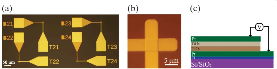
layer, each accessible via a dedicated Pt electrode. Figure 1a illustrates an optical microscope image (top view) of our prototypes with Figure 1b showing a zoom-in image of a single device whose active core occupies an area of 5 × 5 μm2. The schematic cross section of the tested devices is depicted in Figure 1c.
The I-Vcharacteristics of a single device (Figure 1b) was first evaluated via DC sweeping measurements with
)
b
(
)
a
(
Si/SiO
2 TiV
Pt Pt
TiO2
TiOx
(c)
5
µ
m
[image:2.595.61.537.586.705.2]50 µm
Figure 1Optical microscope image, active area, and schematic of different devices. (a)Optical microscope image of a dense stand-alone device;(b)active area of a single 5 × 5μm2device;(c)schematic configuration of the Pt/TiO
the results presented in Figure 2a. During measure-ments, the compliance current was maintained at 1 mA to avoid any destructive process (chemical and/or ther-mal) of the device. For many metal oxide systems, an electroforming step is a prerequisite to facilitate resistive switching [37]. Although the electroforming process
exhibits few negative effects, such as required potentials that are substantially larger from the low-voltage devices' thresholds exhibited by CMOS technologies [38], it also creates a variation of switching parameters [39] and a limitation of the device lifetime. In order to avoid these reported issues in this work, all tested devices were
) c ( )
b ( )
[image:3.595.63.539.90.216.2]a (
Figure 2Resistive and capacitive switching characteristics of Pt/TiO2/TiOx/Pt cells. (a)non-zero crossing I-V characteristic indicating capacitive
capabilities,(b)R-V characteristics of TiO2cell,(c)matching C-V characteristics.
)
b
(
)
a
(
(c)
(d)
[image:3.595.59.540.344.704.2]electrically characterised without any post-treatment electroforming step. Instead of applying one large poten-tial in sweeping mode, we have used sweeping cycles with gradually increasing the range (maximum value) in order to avoid large potentials. For all devices, we ini-tially employ a quasi-static voltage sweep via DC source-measure units (SMU) for acquiring the characteristic
pinched hysteresis I-V loop which is the memristor
signature [1]. Figure 2a illustrates the I-Vcharacteristics when a 5 V bias was swept in steps of 0.1 V within a ± 2 V range. Contrary to the typical signature of an ideal memristor, our device exhibited a bipolar switching re-sponse with a non-zero crossing that occurred at 0.6 V as shown in the inset of Figure 1a, demonstrating the presence of parasitic capacitance in our device.
We have then evaluated our devices' capacity to act as memcapacitors [40], via C-V tests using multi-frequency CVU. More specifically, throughout our measurements, we exploited the configuration where real and imaginary components are connected in parallel [41]. AC imped-ance measurements (1 MHz) of the devices were per-formed with the AC test signal biased with a voltage sweep within the range ±3 V. In this case, the resistance and the capacitance are calculated based on the mea-sured AC impedance and phase. Figure 2b depicts the resistance-voltage (R-V) characteristics of a Pt/TiO2/
TiOx/Pt cell where the arrows indicate the switching
di-rections. A bipolar resistive switching operation was ob-served with a low-resistive state (LRS) and high-resistive state (HRS) respectively attained after the device was biased with positive SET potential of 2.5 V amplitude and negative RESET potential of−3 V. Because the reset did occur with a smooth transition and without a sharp switching, we have considered the value at the end of negative sweeping which is−3 V.
On the other hand, a bipolar capacitive switching trends were also observed as demonstrated in Figure 2c. This device is initially in a low-capacitive state (LCS) and a high-capacitive state (HCS) is attained as the voltage bias approaches VSET =2.6 V. Reversing the voltage polarity, VRESET=−2.7 V causes the device to switch back to LCS.
[image:4.595.304.539.293.674.2]The results indicate that similar SET/RESET potentials are necessary to facilitate both resistive and capacitive switching.
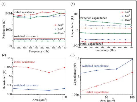
Figure 3a,b depicts the frequency dependence (100 kHz to 1 MHz) of the corresponding resistance and capaci-tance for the initial (pristine) and switched states as a function of devices' active area. These results demonstrate that within this range (100 kHz to 1 MHz), frequency does not play a significant role on either resistive or capacitive states of our devices.
We further investigated the influence of the device's ac-tive area on the resistance and capacitance for both pris-tine (as-fabricated) and switched states. All conductance
(R =1/G) and capacitive measurements were performed via C-V tests by employing 30 mV AC; 1 MHz (DC bias 0.5 V). As shown in Figure 3c, the experimental data do not display any obvious dependence on area, indicating that resistive switching is mainly due to a bulk-based ra-ther than a core/electrode interface mechanism. On the other hand, as expected, the capacitance values for both initial and switched states vary with the electrode areas. It can be observed that small capacitance values (pF range) are defined by a bulk material phenomenon [42,43]. We thus argue that the mechanism responsible for both resist-ive and capacitresist-ive switching is mainly a bulk phenomenon: displacement of the interface between insulating (TiO2
re-gion) and semi-conductive (TiOx) region in the active core
facilitated by migration of the ionic species under applied voltage. It is worth pointing out that minimal disturbance
(a)
(b)
(c)
SET (6V)
RESET (-6V)
C
R
X 8
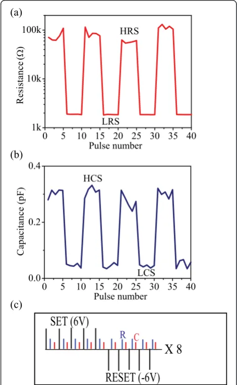
Figure 4Concurrent capacitance/resistance modulation of TiO2-based solid-state devices. (a)Electrical pulse-induced resistance
of the TiO2stoichiometry such as oxygen vacancies act as
n-type dopants or oxygen-excess p-type dopants have a strong impact on the film's resistance and its dielectric properties [44,45]. Various groups have studied the effect of oxygen content on electrical conductivity and demon-strated that the electrical resistance of TiO2 is
propor-tional to the concentration of oxygen [44-47]. On the other hand, it was further proven that the same defects (e.g. oxygen vacancies, excess of oxygen) also affect the di-electric constant of TiO2[48,49]. On that basis, it can be
argued that the TiOx (non-stoichiometric) region has a
different resistance and capacitance than a TiO2
stoichio-metric one. However, the resistive and capacitive states are changed when the applied voltage is strong enough to change the oxygen content within the active core and then the insulated (TiO2) or doped (TiOx) behaviour
domi-nates the overall layer rendering the high or the low resist-ive and capacitresist-ive states.
We further investigated the concurrent resistive and capacitive switching in TiO2-based cells by employing a
voltage-pulsing scheme, as shown in Figure 4c. This bias scheme comprises a train of five SET/RESET voltage
pulses of 6 V/1 μs SET and −6 V/1 μs RESET and the
full sequence is cycled eight times. After each program-ming pulse, the resistance is read by applying a positive pulse of 0.5 V and the capacitance is read via C-V tests at 1 MHz via a small super-imposed sensing signal of
30 mV. The pristine state of TiO2-based devices was
found to be in a HRS and LCS. It should be pointed out that the first positive SET pulse changes the capacitive
state from LCS to HCS and the HRS from 100 MΩ to
100 kΩ(not shown here). Nonetheless, persistent appli-cation of positive SET pulses induced the changes of the resistive state from HRS to LRS and the capacitive state
from HCS to LCS; by applying−6 V RESET pulses, the
HRS and HCS states were restored. The exhibited simul-taneous capacitive and resistive responses of the device are shown in Figure 4a,b.
Contrary with the results presented in [14], here we observe that the switching trend of resistance is corre-lated with that of capacitance, i.e. decrease of capaci-tance with a decrease of resiscapaci-tance. Hence, we argue here that the resistive and the capacitive switching in the investigated devices is mainly induced by the displace-ment of ionic species through the bulk active core.
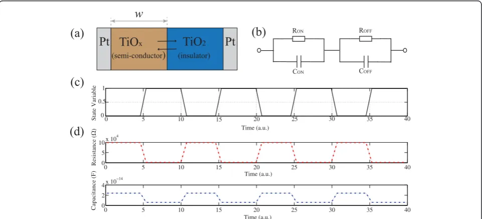
Moreover, Figure 5a illustrates the schematic diagram of the proposed model, i.e. displacement of the interface between doped (TiOx) and undoped (TiO2) regions of
the active core when the voltage is applied. We propose that both layers could be modelled as a series of two parallel RC elements connected as depicted in Figure 5b. In specific, the semi-conductive TiOx layer is
repre-sented by a parallel of RON (1 KΩ) and CON (0.3 pF)
whilst insulating TiO2layer is modelled with high-value ROFF(100 KΩ) andCOFF(0.05 pF). Then, we further
ex-plored the validity of the proposed equivalent circuit
model by evaluating the correlated resistive and
capacitive switching with results shown in Figure 5c. As depicted in Figure 5a, the thickness of the TiOx
layer is ω(t), and the total thickness of the device is D. To simplify, the normalised state variable is defined asx (t) =ω(t)/D. To account for the discontinuous switching
0 5 10 15 20 25 30 35 40
0 5 10x 10
4
Resistance (
Ω
)
0 5 10 15 20 25 30 35 40
0 2 4x 10
−14
Capacitance (F)
RON ROFF
CON COFF
Pt
TiO
xTiO
2Pt
(insulator) (semi-conductor)
(b)
(a)
(c)
0 5 10 15 20 25 30 35 40
0 0.5 1
Time (a.u.)
State Variable
Time (a.u.)
Time (a.u.)
(d)
[image:5.595.58.539.475.693.2]w
in Figure 4, we assume that the drift of the interface be-tween two layers is non-linear and threshold based. In other words, the state variablex(ω(t)/D) would not arise until the activation energies introduced by the external stimulus exceed the corresponding threshold, as depicted in Figure 5c. In this case, the corresponding resistive and capacitive switching trends were simulated and illustrated in Figure 5d, with the simulated results being in good agreement with the measured ones, in support of our argument on the mechanisms of correlated resistive/ capacitive switching.
Conclusions
In conclusion, by using a complete suite of electrical tests, sweeping (DC and AC) and voltage pulsing, we have shown that memristive and memcapacitive effects emerge naturally in nanoscale TiO2elements with their
switching trends being related. TheI-Vcharacteristics of investigated cells display a hysteresis loop with non-zero crossing indicating that our structure also exhibit capacitive effect. Furthermore, the effective resistance and capacitance of TiO2/TiOxMIM devices were modulated simultaneously
by AC sweeping and pulsing modes, rendering resistive and capacitive memory effects in a single device.
Competing interests
The authors declare that they have no competing interests.
Authors’contributions
IS conceived the experiments and performed the electrical characterization. LQ performed the electrical characterization of the samples and simulations. AK fabricated the devices. All authors contributed in the analysis of the results and in the writing of the manuscript. All authors read and approved the final manuscript.
Acknowledgements
The authors wish to acknowledge the financial support of the CHIST-ERA ERA-Net, EPSRC EP/J00801X/1, EP/K017829/1 and National Nature Science Foundation (61171017).
Author details
1Nano Research Group, School of Electronics and Computer Science, University of Southampton, Southampton SO17 1BJ, UK.2College of Electronic Science and Engineering, National University of Defence Technology, Changsha 410073, China.
Received: 21 July 2014 Accepted: 23 September 2014 Published: 4 October 2014
References
1. Chua L:Memristor–the missing circuit element.IEEE Trans Circuit Theory
1971,18:507–519.
2. Nielsen PH, Bashara NM:The reversible voltage-induced initial resistance in the negative resistance sandwich structure.IEEE Trans Electron Devices
1964,11(5):243–244.
3. Simmons JG, Verderber RR:New thin-film resistive memory.Radio Electronic Eng1967,34(2):81–89.
4. Gibbons GF, Beadle WE:Switching properties of thin NiO films.Solid State Electron1964,7(11):785–797.
5. Argall F:Switching phenomena in titanium oxide thin films.Solid State Electron1968,11:535–541.
6. Strukov DB, Snider GS, Stewart DR, Williams RS:The missing memristor found.Nature2008,453:80–83.
7. Kim DC, Seo S, Ahn SE, Suh DS, Lee MJ, Park BH, Yoo IK, Baek IG, Kim HJ, Yim EK, Lee JE, Park SO, Kim HS, Chung UI, Moon JT, Ryu BI:Electrical observations of filamentary conductions for the resistive memory switching in NiO films.Appl Phys Lett2006,88:202102.
8. Lee SB, Lee SJ, Chang SH, Yoo SK, Kang BS, Kahng B, Lee MJ, Kim CJ, Noh TW:
Interface-modified random circuit breaker network model applicable to both bipolar and unipolar resistance switching.Appl Phys Lett2011,98:033502. 9. Hur JH, Lee MJ, Lee CB, Kim YB, Kim CJ:Modeling for bipolar resistive memory switching in transition-metal oxides.PhysRevB2010,82:155321. 10. Wuttig M, Yamada N:Phase-change materials for rewriteable data
storage.Nat Mater2007,6:824–832.
11. Liu S, Wu N, Ignatiev A:Electric-pulse-induced reversible resistance change effect in magnetoresistive films.Appl Phys Lett2000,76:2749–2751. 12. Driscoll T, Kim HT, Chae BG, Kim BJ, Lee YW, Jokerst NM, Palit S, Smith DR,
Di Ventra M, Basov DN:Memory metamaterials.Science2009,325:1518–1521. 13. Yan ZB, Liu JM:Coexistence of high performance resistance and
capacitance memory based on multilayered metal-oxide structures. Sci Rep2013,3:2482.
14. Salaoru I, Khiat A, Li Q, Berdan R, Prodromakis T, Prodromakis T:Pulse-induced resistive and capacitive switching in TiO2thin film devices.Appl Phys Lett 2013,103:233513.
15. Li Q, Khiat A, Salaoru I, Papavassiliou C, Hui X, Prodromakis T:Memory impedance in TiO2based metal-insulator-metal devices.Scientific Report2014,4:4522. 16. Driscoll T, Quinn J, Klein S, Kim HT, Kim BJ, Pershin Yu V, Di Ventra M, Basov
DN:Memristive adaptive filters.Appl Phys Lett2010,97:093502. 17. Yang Y, Ouyang J, Ma L, Tseng RJH, Chu CW:Electrical switching and
bistability in organic/polymeric thin films and memory devices.Adv Funct Mater2006,16:1001–1014.
18. Lau HK, Leung CW:Nonvolatile multilevel memory effect by resistive switching in manganite thin films.J Appl Phys2008,104:123705. 19. Beck A, Bednorz JG, Gerber CH, Rossel C, Widmer D:Reproducible
switching effect in thin oxide films for memory applications.Appl Phys Lett2000,77:139.
20. He C, Shi Z, Zhang L, Yang W, Yang R, Shi D, Zhang G:Multilevel resistive switching in planar graphene/SiO2nanogap structures.ACS Nano2012,
6:4214–4221.
21. Park J, Biju KP, Jung S, Lee W, Lee J, Kim S, Park S, Shin J, Hwang H:Highly scalable non-volatile resistive memory using simple binary oxide driven by asymmetric unipolar voltage pulses.IEEE Electron Device Lett2011,
32(4):476.
22. Wang SY, Huang CW, Lee DY, Tseng TY, Chang TC:Multilevel resistive switching in Ti/CuxO/Pt memory devices.J Appl Phys2010,108:114110. 23. Yang YC, Chen C, Zeng F, Pan F:Multilevel resistance switching in
Cu/TaOx/Pt structures induced by a coupled mechanism.J Appl Phys
2010,107:093701.
24. Chanthbouala A, Garcia V, Cherifi RO, Bouzehouane K, Fusil S, Moya X, Xavier S, Yamada H, Deranlot C, Mathur ND, Bibes MI, Barthélémy A, Grollier J:
A ferroelectric memristor.Nat Mater2012,11:860–864.
25. Schindler C, Thermadam SCP, Waser R, Kozicki MN:Bipolar and unipolar resistive switching in Cu-doped SiO2.IEEE Trans Electron Devices2007,
54:2762–2768.
26. Dong Y, Yu G, McAlpine MC, Lu W, Lieber CM:Si/a-Si core/shell nanowires as nonvolatile crossbar switches.Nano Lett2007,8:386–391.
27. Choi SJ, Park GS, Kim GH, Cho S, Yang WY, Li XS, Moon JH, Lee KJ, Kim K:In situ observation of voltage-induced multilevel resistive switching in solid electrolyte memory.Adv Mater2011,23:3272–3277.
28. Lee MJ, Lee MJ, Han S, Jeon SH, Park BH, Kang BS, Ahn SE, Kim KH, Lee CB, Kim CJ, Yoo IK, Seo DH, Li XS, Park JB, Lee JH, Park Y:Electrical manipulation of nanofilaments in transition-metal oxides for resistance-based memory. Nano Lett2009,9(4):1476–1481.
29. Kim KM, Jeon DS, Hwang CS:Nanofilamentary resistive switching in binary oxide system; a review on the present status and outlook. Nanotechnology2011,22:254002.
30. Schindler C, Szot K, Karthauser S, Waser R:Controlled local filament growth and dissolution in Ag–Ge–Se.PhysStatSol (RRL)2008,2(3):129–131. 31. Ielmini D, Nardi F, Cagli C:Physical models of size-dependent nanofilament
formation and rupture in NiO resistive switching memories.Nanotechnology
2011,22:254022.
32. Gelencser A, Prodromakis T, Toumazou C, Roska T:Biomimetic model of the outer plexiform layer by incorporating memristive devices.PhysRevE
33. Hasegawa T, Ohno T, Terabe K, Tsurvoka T, Nakayama T, Gimzewski JK, Aono M:Learning abilities achieved by a single solid-state atomic switch. Adv Mater2010,22:1831–1834.
34. Zamarreño-Ramos C, Camunas-Mesa L, Zamarreno-Ramos C, Perez-Carrasco JA, Masquelier T, Serrano Gotarredona T, Linares-Barranco B:On spike-timing-dependent-plasticity, memristive devices, and building a self-learning visual cortex.Front. Neurosci.2011,5:26.
35. Salaoru I, Prodromakis T, Khiat A, Toumazou C:Resistive switching of oxygen enhanced TiO2 thin-film devices.Appl Phys Lett2013,102:013506. 36. Nowotny J, Bak T, Burg T:Electrical properties of polycrystalline TiO2at
elevated temperatures. Electrical conductivity.Phys Stat Sol2007,
244:2037.
37. Miao F, Yand YY, Borghetti J, Medeiros-Ribeiro G, Williams RS:Observation of two resistance switching modes in TiO2memristive devices electroformed
at low current.Nanotechnology2011,22:254007.
38. Kaeriyama S, Sakamoto T, Sunamura H, Mizuno M, Kawaura H, Hasegawa T, Terabe K, Nakayama T, Aono M:A nonvolatile programmable solid-electrolyte nanometer switch.IEEE J Solid State Circuit2005,40:168.
39. Liu Q, Long S, Wang W, Zuo Q, Zhang S, Chen J, Liu M:Improvement of resistive switching properties in ZrO2-based ReRAM with implanted Ti ions.IEEE Electron Device Lett2009,30:1336.
40. Di Ventra M, Pershin Y:On the physical properties of memristive, memcapacitive and meminductive systems.Nanotechnology2013,
24:255201.
41. Lee MH, Kim KM, Kim GH, Seok JY, Song SJ, Yoon JH, Hwang CS:Study on the electrical conduction mechanism of bipolar resistive switching TiO2
thin films using impedance spectroscopy.Appl Phys Lett2010,96:152909. 42. Irvine JT, Sinclair DC, West AR:Electroceramics: characterization by
impedance spectroscopy.Adv Mater1990,2(3):132.
43. Sinclair D:Characterization of electro-materials using AC impedance spectroscopy.Bol So cEsp Ceram Vidrio1995,34(2):55–65.
44. Huber B, Gnaser H, Ziegler C:Electrical properties of nanocrystalline anatase TiO2thin films with different crystallite size.Surf Sci2004,
566:419–424.
45. Nowotny J, Radecka M, Rekas M, Sugihara S, Vance ER, Weppner W:
Electronic and ionic conductivity of TiO2single crystal within the n-p
transition range.Ceramics Int1998,24:571–577.
46. Redecka M, Rekas M:Charge and mass transport in ceramic TiO2.J Eur
Ceramic Soc2002,22(12):2001.
47. Bamzai KK, Koohpayeh SM, Kaur B, Fort D, Abell JS:Effect of oxygen content on dielectric properties of float zone grown titanium dioxide (TiO2) crystal.Ferroelectrics2010,377:1–21.
48. Bessergenev V:High temperature phase transition observed in oxygen deficient TiO2−xthin films.ECS Trans2010,25:35–44.
49. Bessergenev V:High temperature anomalies of dielectric constant in TiO2
thin films.Mat Res Bull2009,44:1722–1728.
doi:10.1186/1556-276X-9-552
Cite this article as:Salaoruet al.:Coexistence of memory resistance and memory capacitance in TiO2solid-state devices.Nanoscale Research Letters
20149:552.
Submit your manuscript to a
journal and benefi t from:
7Convenient online submission
7Rigorous peer review
7Immediate publication on acceptance
7Open access: articles freely available online
7High visibility within the fi eld
7Retaining the copyright to your article