N A N O E X P R E S S
Open Access
Investigation of hydrogen plasma treatment for
reducing defects in silicon quantum dot
superlattice structure with amorphous silicon
carbide matrix
Shigeru Yamada
1*, Yasuyoshi Kurokawa
1, Shinsuke Miyajima
1and Makoto Konagai
1,2Abstract
We investigate the effects of hydrogen plasma treatment (HPT) on the properties of silicon quantum dot superlattice films. Hydrogen introduced in the films efficiently passivates silicon and carbon dangling bonds at a treatment temperature of approximately 400°C. The total dangling bond density decreases from 1.1 × 1019cm−3to 3.7 × 1017cm−3, which is comparable to the defect density of typical hydrogenated amorphous silicon carbide films. A damaged layer is found to form on the surface by HPT; this layer can be easily removed by reactive ion etching.
Keywords:Silicon quantum dot; Hydrogen plasma treatment; Defect density; Hydrogen diffusion
PACS:61.46.Hk; 66.30.Pa; 68.65.Hb; 81.65.Cf
Background
Solar cells that use nanomaterials have attracted interest for their potential as ultra-high efficiency solar cells [1]. The conversion efficiency limit of a single-junction solar cell strongly depends on the band gap of the absorber layer, which is known as the Shockley-Queisser limit [2]. To overcome the efficiency limit, various types of quantum dot solar cells, such as quantum size effect type, intermediate band type, and multiexciton gener-ation type, have been proposed [3-5]. The quantum size effect type utilizes the phenomenon that the band gap of a material can be tuned by controlling the diameter of quantum dots, including the periodically arranged narrow-gap quantum dots in a wide-gap dielectric matrix. The fabrication of an amorphous silicon dioxide (a-SiO2) matrix including size-controlled silicon quantum dots (Si-QDs) was reported by Zacharias et al. [6]. The size-controlled Si-QDs can be formed by annealing a superlattice with silicon-rich silicon oxide layers and stoichiometric silicon oxide layers, which is called a silicon quantum dot superlattice structure (Si-QDSL). Since this
report was published, silicon quantum dots embedded in various wide-gap materials, such as amorphous silicon carbide (a-SiC), amorphous silicon nitride (a-Si3N4), and hybrid matrices, have been reported [4,7-11]. Further, the quantum size effect can be observed from the measure-ment of photoluminescence spectra or absorption coeffi-cients [12-14]. The Bloch carrier mobility in a Si-QDSL with an a-SiC matrix is higher than that in a Si-QDSL with an a-SiO2or an a-Si3N4matrix [15]. The barrier height be-tween a-SiC and Si quantum dots is lower than those of the other two materials, resulting in the easy formation of mini-bands [16]. Moreover, the crystallization temperature of a-SiC is lower than those of the other materials. Therefore, in this study, we focus on a Si-QDSL with an a-SiC matrix.
High-temperature annealing above 900°C is needed to fabricate a Si-QDSL with an a-SiC matrix. Several prob-lems, such as dehydrogenation, formation of leakage paths by the crystallization of the a-SiC phase, and dop-ant diffusion in the intrinsic layer of the solar cell struc-ture, occur during high-temperature annealing, resulting in the degradation of solar cell performance. The de-hydrogenation problem has been addressed by hydrogen plasma treatment (HPT) [17]. The crystallization of the a-SiC phase can be prevented by incorporating a small amount of oxygen in the a-SiC matrix [16]. Niobium-* Correspondence:[email protected]
1
Department of Physical Electronics, Tokyo Institute of Technology, Meguro-ku, Tokyo 152-8552, Japan
Full list of author information is available at the end of the article
doped titanium dioxide (TiO2:Nb) can be used as a phosphorus (dopant) diffusion barrier layer for the Si-QDSL solar cell [18]. Using these techniques, an effi-ciency of 0.39% has been achieved in Si-QDSL solar cells fabricated on insulator substrates [19]. Some researchers have reported the electrical properties of silicon quantum dot solar cells [20,21]. However, clear evidence of the con-tribution from Si-QDs has not yet been reported because of poor device quality. To improve device quality, the collection efficiency of the photogenerated carrier should be improved. For this purpose, further reduction of the defect density in the Si-QDSL layers and improvement of the p/i interface is significantly important.
In this study, the dependence of hydrogen concentra-tion and defect density in Si-QDSL films on the process temperature of HPT was investigated. Diffusion coeffi-cients of hydrogen in Si-QDSLs for several treatment temperatures were estimated by secondary ion mass spec-trometry (SIMS). Hydrogen incorporation was also inves-tigated by Raman scattering spectroscopy. In addition, spin densities were measured by electron spin resonance (ESR) spectroscopy, and the optimal temperature was explored. The influence of HPT on the surface of Si-QDSLs was also investigated. The surface morphologies of Si-QDSLs after HPT were measured by atomic force microscopy (AFM), and the thicknesses of the surface damaged layers were estimated by spectroscopic ellipsome-try and cross-sectional transmission electron microscopy
(TEM). The etching of the surface damaged layer was performed by reactive ion etching (RIE) using a tetrafluoro-methane and oxygen (CF4+ O2) gas mixture.
Methods
Forty-period hydrogenated amorphous silicon oxycarbide with a silicon-rich composition (a-Si0.56C0.32O0.12 :H)/hydro-genated amorphous silicon oxycarbide (a-Si0.40C0.35O0.25:H) superlattice was deposited on quartz substrates using very-high frequency plasma-enhanced chemical vapor de-position. The source gases were silane (SiH4), monomethyl-silane (MMS), hydrogen (H2), and carbon dioxide (CO2). The flow rates of MMS, H2, and CO2 were fixed as 1.7, 47.5, and 0.4 sccm, respectively. SiH4 was intermittently flowed during the deposition of silicon-rich layers. Plasma power density, plasma frequency, deposition temperature, deposition pressure, and electrode distance were 13 mW/ cm2, 60 MHz, 193°C, 20 Pa, and 3 cm, respectively. The thicknesses of silicon-rich layers and stoichiometric layers were 5 and 2 nm, respectively. The films were thermally annealed at 900°C for 30 min under a forming gas (3% H2 + 97% N2) atmosphere to form Si-QDs. Film thicknesses of post-annealed samples were 250 ± 10 nm.
[image:2.595.59.538.442.704.2]After annealing, the samples were exposed to hydro-gen plasma to terminate dangling bond defects accom-panying hydrogen atoms in the Si-QDSL. The flow rate of H2, plasma power density, plasma frequency, process pressure, and electrode distance were 200 sccm, 2.60
W/cm2, 60 MHz, 600 Pa, and 3 cm, respectively. The treatment temperature was varied from 200°C to 600°C. To evaluate the hydrogen diffusion coefficient in the Si-QDSL, the samples were treated at 300°C for 20 min, 400°C for 10 min, 500°C for 3 min, and 600°C for 1 min. The depth profiles of the hydrogen concentration were measured by SIMS. In the measurements, Ce+ ions were used to measure the hydrogen depth profiles. Also, the depth was calibrated by the etching rate of the Si-QDSL. Crystalline silicon was used as the standard sample to evaluate the hydrogen concentration. The accuracy of the hydrogen concentration by the SIMS measurement was ± 40%. In addition, for measurements of Raman scattering spectra and ESR, treatment temperature was varied from 200°C to 600°C and the treatment time was fixed at 60 min.
The thicknesses of surface damaged layers formed by 60-min HPT were estimated by spectroscopic ellipsome-try and cross-sectional TEM. The surface morphologies of Si-QDSLs after a 60-min HPT were measured by AFM. The etching of the surface damaged layer was performed by RIE using CF4+ O2 gas (4% O2+ 96% CF4). The gas flow rate, process pressure, and plasma power density were 10 sccm, 4 Pa, and 0.221 W/cm2, respectively. The
surface morphologies after etching were evaluated by AFM and spectroscopic ellipsometry.
Results and discussion
An average hydrogen concentration of 8.2 × 1022 cm−3 was almost uniformly incorporated in the superlattice films before thermal annealing. After annealing at 900°C, the average hydrogen concentration decreased to 1.4 × 1020 cm−3. After HPT, the hydrogen concentration
1 1.5 2 2.5
10-21 10-20 10-19 10-18 10-17 10-16 10-15 10-14 10-13 10-12 10-11 10-10 10-9 10-8 10-7 10-6 10-5 10-4 10-3 10-2
10-11000 800 600 400
1000/T (K 1)
Di
ffu
si
o
n
co
effi
ci
en
t (cm
2 /s
)
T (K)
Experimental data
[image:3.595.59.539.89.394.2]Single crystalline silicon (Wieringen et al.) a-SiC thin film (Schmidt et al.)
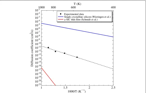
Figure 2Arrhenius plot of diffusion coefficient of hydrogen in Si-QDSLs.The calculated diffusion coefficients of single-crystal silicon by van Wieringen et al. [22] and the estimated diffusion coefficients of an a-SiC thin film with hydrogen concentration of 0.4 ± 0.1 at.% by Schmidt et al. [23] are also described.
200 300 400 500 600
1016 1017 1018 1019
Temperature (oC)
S
p
in de
nsi
ty
(
cm
-3
)
Total-DB Si-DB C-DB
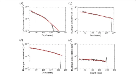
[image:3.595.306.539.570.716.2]increased. Figure 1 shows the depth profiles of hydrogen concentrations of Si-QDSL samples treated at 300°C for 20 min, 400°C for 10 min, 500°C for 3 min, and 600°C for 1 min. The oscillations with small amplitudes in the depth profiles are due to the matrix effect caused by car-bon in the Si-QDSLs. The influence of the matrix effect can be negligible. In addition, structure of the Si-QDSL is almost uniform in the depth direction. Therefore, one can believe the shape of the hydrogen depth profile, which is important to determine the hydrogen diffusion coefficient. The diffusion coefficients can be estimated from these depth profiles. The hydrogen diffusion process follows the diffusion equation
∂C
∂t ¼D
∂2C
∂x2; ð1Þ
where Dis the diffusion coefficient and Cis the hydro-gen concentration at depth x and time t. If the initial hydrogen concentration at all xcan be assumed to zero except for x= 0, and if the hydrogen concentration at
x= 0 can be fixed as C0for t> 0, the following solution is obtained:
C xð Þ ¼;t C0erfc
x 2pffiffiffiffiffiffiDt
; ð2Þ
where the function erfc(z) is a complementary error function. The average diffusion coefficients were esti-mated by fitting the depth profiles with Equation 2. Red lines in Figure 1 indicate the fitting curves based on Equation2. The calculated diffusion coefficients for each temperature were described by dots in Figure 2. The diffusion coefficient obeys Arrhenius law:
D¼D0exp − Δ
E kBT
; ð3Þ
where D0 denotes the preexponential factor, ΔE is the activation energy, and kB is the Boltzmann constant. From the result of the fitting by least squares method, D0 and ΔE were estimated as 3.93 × 10⁻⁷ cm2/s and 0.81 eV, respectively. The calculated diffusion coeffi-cients of single-crystal silicon by van Wieringen et al. [22] and the estimated diffusion coefficients of an a-SiC thin film with hydrogen concentration of 0.4 ± 0.1 at.% by Schmidt et al. [23] are also described in Figure2. D0 and ΔE for single-crystal silicon and the a-SiC thin film are 9.67 × 103 cm2/s and 0.48 eV and 0.71 cm2/s and 3.2 eV, respectively. Compared with these ΔEvalues,ΔE for Si-QDSL is relatively close to the ΔE for single-crystal Si. Such small ΔE indicates that the interstitial diffusion in Si-QDs is dominant because the thickness of the a-SiCO layers is too thin to work as barriers against hydrogen diffusion; this is due to the wide band gap and polar bonds of a-SiC [24].
From the depth profiles of Si-QDSLs for a treatment temperature of 600°C, hydrogen concentration was found to drastically decrease. Saturation hydrogen concentration after sufficient treatment was estimated at approximately 1.0 × 1021cm−3, indicating that the hydrogen concentra-tion at the surface drastically decreases because the loss
1900 2000 2100 2200
Raman shift (cm 1)
N
o
rm
aliz
ed
in
te
n
sity
(
ar
b
. u
n
it)
[image:4.595.57.291.89.267.2]200 oC 300 oC 400 oC 500 oC 600 oC
Figure 4Raman spectra of Si-QDSLs after a 60-min HPT.
[image:4.595.56.540.582.714.2]of adsorbed hydrogen atoms is dominant at high temperatures.
The defect densities of Si-QDSLs after 60-min HPT for several treatment temperatures were measured by ESR. The defect densities originating from silicon dangling bonds (Si-DBs) and carbon dangling bonds (C-DBs) were also estimated. The waveform separation of the obtained differentiated waves originating from both Si-DBs and C-DBs were so difficult that the ratios between the dens-ities of Si-DBs and C-DBs were estimated by the following equations [25]:
g xð ;γÞ ¼X12
n¼0
1−x
ð ÞgSið Þ þn xγgCð Þn
1−x
ð Þ þxγ 12Cnx
nð1−xÞ12−n
;
ð4Þ
NSi−DB¼ 1
1þγNTotal−DB ð5Þ
and
NC−DB¼ γ
1þγNTotal‐DB; ð6Þ
where NTotal-DB, NSi-DB, and NC-DB are the densities of total dangling bonds (Total-DBs), Si-DBs, and C-DBs, respectively.yis the ratio ofNC-DBtoNSi-DBandxis the composition ratio of C to Si.gSið Þn is the averagegvalue
of Si-DB surrounded by (12−n) Si atoms and n C atoms, gCð Þn is the average g value of a C-DB
sur-rounded by (12−n) Si atoms andnC atoms, andg(x,y) is the measured g value. Although this expression is de-rived for an a-Si1-xCxalloy system, it is believed to be valid for Si-QDSL with an a-SiC matrix, which can be consid-ered as an approximately homogeneous material, since the dangling bond defect density in Si-QDs is much lower than that of the a-SiC matrix, and the dangling bonds on Si-QD surfaces are passivated by the a-SiC matrix. An average composition ratio of 0.40 was used.
NTotal-DB,NSi-DB, andNC-DBfor several treatment tem-peratures are shown in Figure 3. Post-HPT, Si-QDSL de-fect density (1.1 × 1019 cm−3) clearly reduced compared with the defect density before HPT. The defect density for 200°C treatment is still high because hydrogen diffu-sion is insufficient. Hydrogen intrudiffu-sion depth for 60-min HPT can be estimated to be below 100 nm, and a several dangling bonds remain in the deep area of the film. The defect density for 300°C treatment is lower than that at 200°C. A large amount of hydrogen reaches the interface of the film and substrate during the 60-min HPT. The measured g value in this sample was 2.00275, which is quite similar to the g value of C-DB, meaning that NSi-DB is less than NC-DB. Based on Equation 5, NSi-DB is estimated to be 2.2 × 1016 cm−3, indicating that Si-DBs can be efficiently passivated by the incorporated
[image:5.595.306.539.110.168.2]hydrogen. For the 400°C treatment, defect density de-creases to 3.7 × 1017cm−3, which is comparable with the defect density of an a-SiC film. The g value for 400°C treatment was higher than that for 300°C treatment, indicating that C-DBs - which are dominant in the total-DBs - significantly decrease despite the increment in Si-DBs. For the 500°C treatment, defect density increases despite efficient hydrogen incorporation in the Si-QDSL, showing that the hydrogen atoms are thermally activated from the Si-H bond state to the interstitial state above 300°C and from the C-H bond state to the interstitial state above 400°C. These temperatures mostly corres-pond to the temperatures of dehydrogenation from Si-H bonds and C-H bonds, which are approximately above 300°C [26] and 450°C to 550°C [27], respectively. In the 500°C treatment sample, a large amount of hydrogen atoms were in the interstitial sites; they did not contrib-ute to the passivation of the dangling bonds.
Figure 4 shows the Raman spectra of the Si-QDSLs after 60-min HPT at different temperatures. The peak found between 2,000 and 2,100 cm−1corresponds to the Raman shift originating from the stretching mode of Si-Hnbonds. The intensity of the peak from Si-Hnbonds gradually weakens as the treatment temperature in-creases, indicating that the Si-Hnbonds decomposed by the thermal activation of terminal hydrogen atoms. This trend agrees with the increment ofNSi-DB.
[image:5.595.58.289.230.355.2]During HPT, the surface is damaged by atomic hydro-gen. The thickness of the surface damaged layer is Table 1 Thicknesses estimated by fitting of the
spectroscopic ellipsometry measurements of Si-QDSLs
Parameters 300°C 400°C 500°C 600°C
MSE 11.56 12.22 13.37 13.30
Ts(nm) 33.1 11.5 15.2 6.5
T(nm) 167.7 212.8 224.7 246.1
300 400 500 600
0 10 20 30
40 (ellipsometry)
RMS (AFM)
Temperature (
oC)
T
h
ic
k
n
ess (
n
m)
Ts
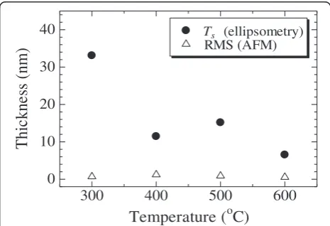
[image:5.595.305.538.546.705.2]dependent on the treatment temperature. The thickness of the surface damaged layer was estimated by spectro-scopic ellipsometry. A schematic of the structure used for the analysis is shown in Figure 5. The Tauc-Lorentz model was applied to the optical modeling of the Si-QDSL layer, and the surface damaged layer was assumed to be the effective medium approximation (EMA) layer in which 50% void exists. The estimated thicknesses of the Si-QDSL layers T, the thicknesses of the surface damaged layersTs, and the mean square error (MSE) of each fitting are summarized in Table 1. Ts of an as-annealed Si-QDSL was approximately 2 nm, while the
Tsof the treated Si-QDSLs drastically increased, indicat-ing that the Si-QDSL structure in the surface region was broken by the atomic hydrogen.
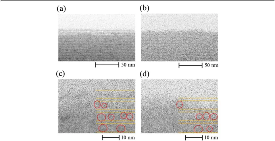
[image:6.595.58.537.89.334.2]The thicknesses T and Ts strongly depend on the treatment temperature. T decreases as the treatment temperature increases; this tendency is related to the hydrogen concentration at the near-surface for each treatment temperature. A large amount of hydrogen introduced into amorphous silicon contributes to the structural reconstruction by breaking the weak Si-Si bonds [28,29]. Further, surface morphologies were mea-sured by AFM. The root mean square (RMS) surface roughness of the samples is shown in Figure 6. RMS sur-face roughness is almost independent of the treatment temperature, whereas the damaged layer thickness measured by spectroscopic ellipsometry decreased with treatment temperature, indicating that HPT at low temperature introduces a damaged layer with lower refractive index than that of Si-QDSL. To investigate further, TEM observations of the Si-QDSLs were con-ducted. Figure 7a,b shows TEM images of the 350°C and
Figure 7Cross-sectional TEM images.At the near-surface of(a)350°C treatment sample,(b)600°C treatment sample,(c)magnified image of 350°C treatment sample, and(d)magnified image of 600°C treatment sample.
300
400
500
600
0
1
2
3
4
5
(ellipsometry) RMS (AFM)
Temperature (
oC)
Thi
ckne
ss (
n
m
)
Ts [image:6.595.57.291.536.704.2]Figure 8RMS roughness measured by AFM and thicknesses of the surface damaged layers of Si-QDSLs after RIE.
Table 2 Thicknesses estimated by fitting of the spectroscopic ellipsometry measurements of surface-etched Si-QDSLs
Parameters 300°C 400°C 500°C 600°C
MSE 14.94 10.80 14.72 15.90
Ts(nm) 1.9 1.4 2.8 2.1
[image:6.595.306.539.677.734.2]600°C treatment samples, and Figure 7c,d shows the magnified images of each sample. In the magnified images, existence of the Si-QDs is indicated using red circles. The irradiated electrons are transmitted through the sample without scattering in the white region, show-ing that the material density at the near surface is ex-tremely low in the white region. Detailed analysis of the TEM images revealed that the two periods of superlat-tice layers were completely removed by 350°C HPT. Two or three periods of superlattice layers were found to be damaged. On the other hand, for the 600°C treat-ment sample, no removal of the layers was observed during the HPT treatment; only the one-period superlat-tice layer was damaged. This result agrees with the thickness of the damaged layer estimated by the spectro-scopic ellipsometry.
The damaged layer is defective and no longer acts as a Si-QDSL. Therefore, the existence of the damaged layer is a cause of the degradation of Si-QDSL solar cell per-formance. The removal of the damaged layer without additional damage is very important. Therefore, etching of the damaged layer was performed using RIE. RMS roughness measured by AFM and the damaged layer thicknesses estimated by spectroscopic ellipsometry of the Si-QDSLs after RIE are shown in Figure 8. The esti-mated thicknesses of the Si-QDSL layers T, the thick-nesses of the surface damaged layersTs, and the MSE of each fitting are summarized in Table 2. The observed RMS roughness was less than 3 nm, which was almost the same as that of the sample before RIE. The thick-nesses of the surface damaged layers estimated by spec-troscopic ellipsometry were almost the same as those of the RMS roughness. In general, surface roughness is also modeled using the EMA model for ellipsometry analysis; thus, the estimatedTsreflects surface roughness, and no damaged layer exists on the surface. These results clearly indicate that RIE can remove the damaged layer without additional damage to the sample; RIE is therefore the key to improve the film quality of Si-QDSLs and the p/i interface in Si-QDSL solar cells.
Conclusions
Hydrogen plasma treatment temperature dependences of defect densities and hydrogen concentrations in Si-QDSLs as well as the surface morphologies of Si-QDSLs were investigated. Hydrogen could be quickly incorporated as the treatment temperature increases. On the other hand, dehydrogenation of hydrogen atoms terminating the dangling bonds is dominant during high-temperature treatments. The optimal treatment temperature was found to be approximately 400°C, and a defect density of 3.7 × 1017 cm−3was achieved, which is comparable to the defect density of a typical a-SiC:H film. In addition, damaged layer was found to form on
the surface by HPT; this damaged layer can be easily re-moved by RIE without additional damage to the sample. Thus, HPT and damaged layer removal process are very important for the fabrication of Si-QDSL solar cells.
Competing interests
The authors declare that they have no competing interests.
Authors’contributions
SY carried out the experiments and the calculations. MK supervised the work and finalized the manuscript. YK and SM participated in the design of the study and helped to draft the manuscript. All authors read and approved the final manuscript.
Acknowledgements
This work was supported in part by the New Energy and Industrial Technology Development Organization (NEDO) under the Ministry of Economy Trade and Industry of Japan.
Author details
1Department of Physical Electronics, Tokyo Institute of Technology,
Meguro-ku, Tokyo 152-8552, Japan.2Photovoltaics Research Center (PVREC),
Tokyo Institute of Technology, Meguro-ku, Tokyo 152-8552, Japan.
Received: 19 December 2013 Accepted: 4 February 2014 Published: 12 February 2014
References
1. Conibeer G, Green MA, Corkish R, Cho Y-H, Cho E-C, Jiang C-W, Fangsuwannarak T, Pink E, Huang Y, Puzzer T, Trupke T, Richards B, Shalav A, Lin K-L:Silicon nanostructures for third generation photovoltaic solar cells.Thin Solid Films 2006,511:654.
2. Shockley W, Queisser HJ:Detailed balance limit of efficiency of p-n junction solar cells.J Appl Phys1961,32:510.
3. Beard MC, Knutsen KP, Yu P, Luther JM, Song Q, Metzger WK, Ellingson RJ, Nozik AJ:Multiple exciton generation in colloidal silicon nanocrystals.
Nano Lett2007,7:2506.
4. Green MA:Third generation photovoltaics and feasibility of realization.
InTech Dig of the 15th International Photovoltaic Science and Engineering Conference: 10–15 Oct 2005.Shanghai:7.
5. Hanna MC, Nozik AJ:Solar conversion efficiency of photovoltaic and photoelectrolysis cells with carrier multiplication absorbers.J Appl Phys 2006,100:074510.
6. Zacharias M, Heitmann J, Scholz R, Kahler U, Schmidt M, Bläsing J:
Size-controlled highly luminescent silicon nanocrystals: a SiO/SiO2
superlattice approach.Appl Phys Lett2002,80:661.
7. Cho Y-H, Cho E-C, Huang Y, Jiang C-W, Conibeer G, Green MA:Silicon quantum dots in SiNxmatrix for third generation photovoltaics.InProc 20th European Photovoltaic Solar Energy Conference.Barcelona; 2005:47. 8. Kurokawa Y, Miyajima S, Yamada A, Konagai M:Preparation of
nanocrystalline silicon in amorphous silicon carbide matrix.Jpn J Appl Phys Part 22006,45:L1064.
9. Song D, Cho E-C, Cho Y-H, Conibeer G, Huang Y, Huang S, Green MA:
Evolution of Si (and SiC) nanocrystal precipitation in SiC matrix.Thin Solid Films2008,516:3824.
10. Di D, Perez-Wurfl I, Conibeer G, Green MA:Formation and photolumines-cence of Si quantum dots in SiO2/Si3N4hybrid matrix for all-Si tandem
solar cells.Sol Energy Mater Sol Cells2010,94:2238.
11. Ding K, Aeberhard U, Astakhov O, Köhler F, Beyer W, Finger F, Carius R, Rau U:Silicon quantum dot formation in SiC/SiOxhetero-superlattice. Energy Procedia2011,10:249.
12. Kurokawa Y, Tomita S, Miyajima S, Yamada A, Konagai M:Photoluminescence from silicon quantum dots in Si quantum dots/amorphous SiC superlattice.
Jpn J Appl Phys Part 22007,46:L833.
13. Hartel AM, Gutsch S, Hiller D, Zacharias M:Fundamental temperature-dependent properties of the Si nanocrystal band gap.Phys Rev B2012,
85:165306.
15. Jiang C, Green MA, Silicon quantum dot superlattices:Modeling of energy bands, densities of states, and mobilities for silicon tandem solar cell applications.J Appl Phys2006,99:114902.
16. Kurokawa Y, Yamada S, Miyajima S, Yamada A, Konagai M:Effects of oxygen addition on electrical properties of silicon quantum dots/amorphous silicon carbide superlattice.Curr Appl Phys2010,10:S435.
17. Kurokawa Y, Tomita S, Miyajima S, Yamada A, Konagai M:Observation of the photovoltaics effect from the solar cells using silicon quantum dots superlattice as a light absorption layer.InProc 33rd IEEE Photovoltaic Specialists Conference.San Diego; 2008:211.
18. Yamada S, Kurokawa Y, Konagai M:High thermostable ad conductive niobium doped titanium oxide for the application to a diffusion barrier layer of silicon quantum dot superlattice solar cell structure.InProc 37th IEEE Photovoltaic Specialists Conference.Seattle; 2011:2113.
19. Yamada S, Kurokawa Y, Miyajima S, Konagai M:Improvement of electrical properties of silicon quantum dot superlattice solar cells with diffusion barrier layers.Jpn J Appl Phys2013,52:04CR02.
20. Perez-Wurfl I, Ma L, Lin D, Hao X, Green MA, Conibeer G:Silicon nanocrystals in an oxide matrix for thin film solar cells with 492 mV open circuit voltage.Sol Energy Mater Sol Cells2012,100:65. 21. Löper P, Canino M, Qazzazie D, Schnabel M, Allegrezza M, Summonte C,
Glunz SW, Janz S, Zacharias M:Silicon nanocrystals embedded in silicon carbide: investigation of charge carrier transport and recombination.
Appl Phys Lett2013,102:033507.
22. Van Wieringen A, Warmholtz N:On the permeation of hydrogen and helium in single crystal silicon and germanium at elevated temperatures.Physica1956,22:849.
23. Schmidt H, Borchardt G, Geckle U, Bruns M, Baumann H:Comparative study of trap-limited hydrogen diffusion in amorphous SiC, Si0.66C0.33N1.33, and
SiN1.33films.J Phys Condens Matter2006,18:5363.
24. Robertson J:Defect densities and hydrogen diffusion in hydrogenated amorphous Si-based alloys.Appl Phys Lett1991,59:3425.
25. Ishii N, Kumeda M, Shimizu T:A simple molecular orbital calculation of ESR g-values for amorphous Si1-xCx, Si1-xGexand Ge1-xCx.Sol Stat Comm 1982,41:143.
26. Tsai CC, Fritzsche H:Effect of annealing on the optical properties of plasma deposited amorphous hydrogenated silicon.Sol Energy Mater Sol Cells1979,1:29.
27. Vasin AV, Kolesnik SP, Konchits AA, Kushnirenko VI, Lysenko VS, Nozarov AN, Rusavsky AV:Effects of hydrogen bond redistribution on photoluminescence of a-SiC:H films under thermal treatment.J Appl Phys2006,99:113520. 28. Street RA:Metastability and the hydrogen distribution in aSi:H.
AIP Conf Proc1991,234:21.
29. Shirai H, Hanna J, Shimizu I:Role of atomic hydrogen during growth of hydrogenated amorphous silicon in the“chemical annealing”.
Jpn J Appl Phys1991,30:L679.
doi:10.1186/1556-276X-9-72
Cite this article as:Yamadaet al.:Investigation of hydrogen plasma treatment for reducing defects in silicon quantum dot superlattice structure with amorphous silicon carbide matrix.Nanoscale Research Letters20149:72.
Submit your manuscript to a
journal and benefi t from:
7Convenient online submission
7Rigorous peer review
7Immediate publication on acceptance
7Open access: articles freely available online
7High visibility within the fi eld
7Retaining the copyright to your article