FEB-MAR, 2015. VOL-II/XVII www.srjis.com Page 2216 CHALLENGES IN PHYSICAL DESIGN AT BLOCK LEVEL
Mr. Navandar Rajesh Kedarnath1 & Deokar Subhash Mahadeo2, Ph. D.
Technology scaling has been increasing in semiconductor and thereby EDA industry. Nowadays, 28nm CMOS designs are in full production and 16nm design rules and infrastructure are already in place for designs starting later this year. Design productivity and increasing cost of doing design have become a major issue in large scale design projects. In addition, now that the physical limits are beginning to impact scaling [11], the question is: What are the challenges at 28nm and what would design look like going into 28nm and beyond? In this paper, we will focus on the major design and CAD challenges associated with 28nm and beyond.
Keywords— Physical design, 28nm technology, NDR, Multicycle path, Congestion
I. INTRODUCTION
The combination of a high performance, low-power process with architectural innovations
and cost-effective mass production possibilities, makes 28nm [11] process well suited for
power sensitive applications, bandwidth-intensive, and high-end applications. Each
advancement in process technology results larger numbers of process layers and transistors,
requiring more design and manufacturing rule checks before manufacturing handoff. This
results increase in physical verification runtime and increase in violations analysis, tape-outs
deadlines and time to market. The size and complexity of modern designs add another crucial
challenge to the current physical design verification technology. Designers need more
effective and fast physical verification capabilities in order to deliver accurate results required
to keep projects on track. The difficult task cost of mask sets for manometer processes creates
additional pressure to detect and correct errors as early as possible in the physical-verification
[11] process. Longer physical verification cycles can delay time-to-market, but incomplete
rule checking can reduce yield, degrade reliability, and invalidate functionality. The
combination of complex rules, more transistors, and extra levels of wiring presents a
powerful challenge to today's physical-verification tools, especially when dealing with 28nm
FEB-MAR, 2015. VOL-II/XVII www.srjis.com Page 2217 a signal through them at speeds approaching more than one gigahertz. The low-power [11],
28nm technology platform can provide power, performance and time-to-market advantages
for producers of a broad range of power-sensitive mobile and consumer electronics
applications.
II. CHALLENGES AND THEIR SOLUTIONS
Here are some challenges which are being faced in 28nm technology.
A. Block Size
As technology has been scaling, die size is also reducing and no. of gate counts has been
increasing. So in order to get filled all the standard cells properly in the core area and to do
the best floorplan, the block size should be well proper in order to meet these conditions. Not
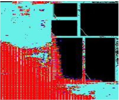
[image:2.595.182.428.319.584.2]meeting these conditions can lead to bad timing and congestion problems.
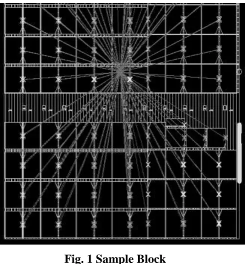
Fig. 1 Sample Block
Here in the Fig. 1 sample block has been shown. This block contained 100+ macros &
2 clock channels [6] in between them. The size of the block was so complicated to place all
the macros well accordingly. There were lot of issues in this block like Congestion, High
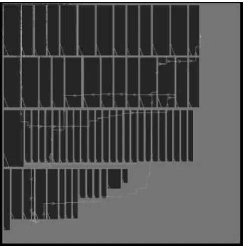
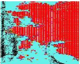
FEB-MAR, 2015. VOL-II/XVII www.srjis.com Page 2218 Fig. 2 Sample block
Here in the Fig. 2 and Fig. 3 sample blocks has been shown which was containing 75+
macros. In Fig. 3 sample block there was an issue of high WNS. In this Fig the reg2reg path
is violating which is shown as yellow path.
Fig. 3 Sample block
B. NDR (Non Default Routing)
Non default rule [3] is a routing rule that is usually consists of width and
[image:3.595.184.428.417.662.2]FEB-MAR, 2015. VOL-II/XVII www.srjis.com Page 2219 you to adjust spacing and width to lower coupling cap, resistance, etc. in order to improve
performance. In 45nm and below technology shielding the clocks is more important than
ever in order to avoid noise on the clock nets.
C. Instance Grouping
Instance grouping is a one kind of technique to guide the tool for placing the particular
instance group in particular region. Some times tool is not doing its job for placing the
instance in the block as we want. So, at that time we have to guide it for placing the instance
to achieve the good timing.
There are two types of Instance grouping.
1) Soft grouping
2) Hard grouping
In soft grouping the tool will also think about the timing and has also flexibility to move
the instances out of that region, while in hard grouping tool will place the instances in the
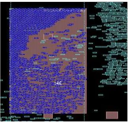
defined region only. Here the hard grouping is as shown as in Fig.4.
In the Fig the pink region in which standard cells are getting placed is the hard grouping
region. The standard cells which are highlighted using blue colour are the module for which
the hard grouping area was created. So in hard grouping standard cells will place in the
defined region only while in soft grouping the standard cells can be place out of the defined
[image:4.595.201.409.473.671.2]region also to meet the timing.
Fig. 4 Hard grouping of standard cells
D. Logic Cone
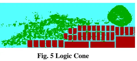
Sometimes one register is talking to thousands of registers. So at that time it might not be
FEB-MAR, 2015. VOL-II/XVII www.srjis.com Page 2220 spread out the registers and it may place them far from the main register which may lead to
timing problem. This problem can be solving by doing changes in netlist. Here is an example
for the logic cone as shown in Fig 5. Here we can see that logic between registers is
[image:5.595.188.426.150.256.2]spreading.
Fig. 5 Logic Cone
E. Moving IO Pins
At one point of time in the design we found that timing is degraded and macros were
placed well enough. At that time after an enough analysis we can relocate the IO pins this
will also help a lot at some time.
F. Adding Flops or Multicycle Path
Multicycle paths are data paths that require more than one clock cycle to latch data at the
destination register. For example, a register may be required to capture data on every second
or third rising clock edge. In the design if we have very huge WNS for any module and if that
module is related to any testing module then we can tell RTL guy to add one more flop in
between to meet the timing.
G. Congestion
Routing congestion [6] occurs when too many routes need to go through an area that does
not have enough resources or routing tracks to accommodate them.
Process geometries below 28nm [5] enable more common place use of high density cells,
whose cell heights dictate a decrease from 10-12 routing tracks through them to just 9. This
means there are even fewer routing resources per cell, which will make the congestion
problem even more. The use of pins on the “metal 2” layer is becoming more common,
providing easier pin access but it is decreasing routing resources. And more metal resources
must be dedicated to the power grid for higher power densities, higher frequencies, or
complex power architectures such as multi-supply voltage. This means fewer resources for
FEB-MAR, 2015. VOL-II/XVII www.srjis.com Page 2221 Fig. 6 Congestion Cycle
The delay impact of wires in below 28nm [5] technology, modern timing aware routers
will try as much as possible to detour only those routes on non timing critical paths. But this
is not always possible. But in this technology it is likely that a non-critical path becomes
critical after its route is detoured. And because of that tool is tend to buffer those detoured
routes in an attempt to speed them up, and this can create further congestion [7]. So
congestion creates more timing failures because the only reason these paths fail is due to long
physical wires that result from detoured routes. Congestion can also happen when the
standard cells are dense so close with each other in a limited area. The high density issue can
be solved by specifying density in the particular region.
1). Floorplan congestion
This occurs when the floorplan [7] has macros and other routing blockages that are too
close together to get enough routes through to connect to the macros. For instance, the
congestion [8] can occur in slots between memories or around corners of memories. Here Fig.
7 and 8 shows the examples for the floorplan congestion.
[image:6.595.197.399.490.659.2]FEB-MAR, 2015. VOL-II/XVII www.srjis.com Page 2222 Fig. 8 Example of Floorplan congestion
2). Placement Density Congestion
Placement [8] utilization is basically how densely the cells are placed. When there are too
many cells too close together, then routing all the connections between them creates
congestion. This can lead to high utilization for any design. This can also happen when
timing is tightly constrained, causing timing-driven placement [8] to place these cells closer
together. This can be netlist issue also if netlist has been poorly constructed. This type of
congestion is dependent on the quality of the netlist, floorplan and placement. Here Fig. 9
shows the example for the placement density congestion.
Fig. 9 Example of Placement density congestion
3). Fixing Congestion
Fixing congestion starts with identifying that congestion is the problem and then
determining the root cause. Congestion is dependent on the floorplan, placement quality and
utilization. The only way to fix floorplan [10] [8] congestion is to change the floorplan. This
can be done by creating more space around the macros, creating placement blockages, or
rearranging the macro placement or orientation is often solutions.
For fixing placement [8] density congestion, a first step is to look at reducing the amount
[image:7.595.221.375.439.563.2]FEB-MAR, 2015. VOL-II/XVII www.srjis.com Page 2223 Also, if synthesis was performed with inaccurate wire delay models, then we may have to
remove buffers and inverter pairs before placement.
If these types of fixes cannot be performed, then placement [7] utilization should be taken
in to mind. Decreasing the overall target utilization for a chip is often the least desirable
approach, because it will lead to increase the die size.
RESULTS & SUMMARY
Placement Routing
Blocks Paths WNS TNS WNS TNS
Block_1
Reg2reg
-0.271 -90.615 -0.113 -6.384
In2reg
-0.366
-0.792
-0.433 -11.075
Reg2out
-0.510
-1.337
-0.431
-1.095
Block_2
Reg2reg
-0.191 -61.570 -0.163 -25.552
In2reg
-0.085
-0.24
-0.084
0.238
Reg2out
-0.147 -23.028 -0.049 -0.331 Block_3
Reg2reg
-0.120 -65.194
-0.1
-13.919
Reg2out
-0.149
-0.612 0.093 --0.265
Reg2reg
-0.229 -38.571 -0.143 -6.942
Here in the table Placement & Routing WNS & TNS has been shown for three blocks
according to three different violating paths. The major issue in these sample blocks were
floorplan, High logic cone & congestion.
REFERENCES
G.G. Shahidi, “Device Scaling for 15nm Node and Beyond”, Proc. 2009 Dev. Res. Conf., pp. 247, 2009.
R. Puri et al, “The Dawn of 22nm Era: Design and CAD Challenges”, Proc. 2010 Conf. VLSI Des., pp. 429, 2010.
FEB-MAR, 2015. VOL-II/XVII www.srjis.com Page 2224 Frank, D.J., Puri, R., Toma, Dorel “Design and CAD Challenges in 45nm CMOS and beyond”,
Computer-Aided Design, 2006. ICCAD '06. ACM International Conference, pp. 329, 2006. Dautriche, P., “Analog design trends and challenges in 28 and 20nm CMOS technology”, Proc. 2011
Solid-State Device Research Conf. , pp. 1, 2011.
Chakrabarti, P., “Clock Tree Skew Minimization with Structured Routing”, Proc. 2012 VLSI Design (VLSID), pp. 233, 2012.
Fubing Mao , Yuchun Ma , Ning Xu , Shenghua Liu , “Congestion-driven floorplanning based on two-stage optimization”, Proc. 2009 ASICON '09, pp. 1298, 2009.
M. Wang, X. Yang, and M. Sarrafzadeh, “Congestion minimization during placement,” IEEE Transactions of Computer-Aided Design, vol. 19, pp. 1140, 2000.
M. Wang, and M. Sarrafzadeh, “Modeling and minimization of routing congestion,” Asia and South Pacific Design Automation Conference, pp. 185, 2000.
M.Wang and M. Sarrafzadeh, "On the behavior of congestion minimization during placement," in Proc. Int. Symp. Physical Design, Apr. 1999, pp. 145, 1999.