Chromatography System
Thesis by
Victor Chi-Yuan Shih
In Partial Fulfillment of the Requirements for the Degree of
Doctor of Philosophy
California Institute of Technology Pasadena, California
2006
© 2006
Victor Chi-Yuan Shih
Acknowledgements
My advisor, Dr. Yu-Chong Tai, made my Ph.D. study the most significant and fruitful experience in my life. Working with Dr. Tai day in and day out for five years, I was amazed by his wisdom in making the right decisions, doing the right things at the right time. He showed me the art of managing things according to priority, by which one’s limited time and energy can be leveraged to maximize achievements. Although extremely demanding on research, Dr. Tai has never failed to cheer us up with optimism and a sense of humor when reality showed cold faces to our efforts. Dr. Tai makes our Lab a fun place to work with his fairness to people, generosity, and unique fearless leadership. I was so lucky to work with him and have a mentor like him.
My parents have given me tremendous support in every aspect and stage of my life. They worked hard and saved every possible penny to provide the best environment and resources for their children. Being away from them for many years, I often regretted that I was not able to appreciate more their love and share their hardship in my young years. This thesis is dedicated to them, as a present for their sixtieth birthdays. Dear dad and mom, I have missed you so much these years and happy birthday to you!
to cook all kinds of delicious food made my dining time the happiest of every day. With her faith in me, I have overcome bad times and failures. Most important of all, my efforts in life are all worth it when she is beside me to share the joys. I am the luckiest man to have met her and to have her as my wife. (Vanessa, I love you!)∞.
I would also like to thank the current and previous members of the Caltech Mircromachining Laboratory who have given me advice and help. Mr. Trevor Roper is a respectful technician from whom I have learned tremendously. It has always been a wonderful experience working with him inside the cleanroom. Mrs. Christine Matsuki and Mrs. Tanya Owen are very nice secretaries and their help has extensively facilitated my research. Dr. Tze-Jung Yao, Dr. Yong Xu, Dr. Ellis Meng, Dr. Jun Xie, Dr. Qing He, Dr. Matthieu Liger, Dr. Justin Boland, and Mr. Ted Harder have given me great advice in research and have been good friends of mine over the years. Special thanks are dedicated to Dr. Yao, who introduced me to this lovely lab, and Dr. Xie, with whom I had so many fruitful research discussions. My colleagues in our lab, Scott Miserendino, Changlin Pang, Angela Tooker, Siyang Zheng, Damien Rodger, Po-Jui Chen (we shared so much fun), Quoc Quach, Wen Li, Nick Lo, Jason Shih, and Mike Liu are wonderful working company. Yang Chen and Wei Li are outstanding Caltech undergrads with whom I have worked. I will never forget the joyful memories we shared over the years.
Abstract
Temperature-Controlled Microchip Liquid
Chromatography System
Thesis by Victor Chi-Yuan Shih
Doctor of Philosophy in Electrical Engineering California Institute of Technology
Table of Contents
Chapter 1 MEMS Technology... 1
1.1 Introduction... 1
1.1.1 MEMS by Definition ... 1
1.1.2 MEMS Fabrication Technology... 2
1.1.2.1 Bulk Micromachining ... 2
1.1.2.2 Surface Micromachining... 6
1.1.2.3 Other Technologies ... 6
1.1.2.4 Summary ... 8
1.1.3 Market and Products of MEMS Technology ... 9
1.2 Lab-on-a-Chip System by MEMS Technology ... 12
1.2.1 Applications of Lab-on-a-Chip System ... 12
1.2.2 Challenges and Outlooks ... 14
1.3 Parylene as a Microstructure Material... 16
1.3.1 Introduction to Parylene ... 16
1.3.2 Applications of Parylene Thin Film in MEMS... 20
1.4 Bibliography ... 22
Chapter 2 Evolution of HPLC Technology
... 282.1 High-Performance Liquid Chromatography... 28
2.1.1 Introduction... 28
2.1.2 History ... 30
2.1.3 Theory... 32
2.1.3.1 Analyte Retention and Chromatogram... 32
2.1.3.2 Height Equivalent to a Theoretical Plate ... 36
2.1.3.4 Band-Broadening Phenomenon ... 38
2.2 HPLC Instrumentation... 42
2.2.1 Separation Column ... 42
2.2.1.1 Separation Column Tube... 42
2.2.1.2 Separation Column Packing Material ... 43
2.2.2 Solvent Pumps ... 45
2.2.3 Sample Injection Valves ... 46
2.2.4 Analyte Detectors ... 46
2.3 Logical Trend of HPLC Instrumentation... 49
2.3.1 Predictions from the Theory ... 49
2.3.2 Benefits of Microchip HPLC System ... 50
2.4 Review of Microchip HPLC Systems... 51
2.5 Comparisons bewteen LC and CE... 53
2.6 Conclusions... 56
2.7 Bibliography ... 57
Chapter 3 High-Pressure Microfluidic Channel Technology
... 623.1 Introduction... 62
3.2 Review of Microfluidic Channel Technology… ... 63
3.2.1 PDMS Microfluidic Channel... 63
3.2.2 Thermal-Bonding Microfluidic Channel ... 64
3.2.3 Nitride Microfluidic Channel ... 64
3.2.4 Parylene Microfluidic Channel... 65
3.2.5 Buried Microfluidic Channel... 66
3.3 High-Pressure Parylene Microfluidic Channel Technology ... 68
3.3.1 Anchored-Type Parylene Microfluidic Channel... 68
3.3.3 Comparisons ... 73
3.4 Conclusions... 73
3.5 Bibliography ... 75
Chapter 4 Temperature-Controlled Microchip HPLC System... 78
4.1 Temperature Gradient Interaction Chromatography... 78
4.2 Chip Design, Fabrication, and, Characterization... 81
4.2.1 Low-Power, Low-Pressure-Capacity System ... 81
4.2.1.1 Design and Fabrication ... 81
4.2.1.2 System Characterization... 83
4.2.2 High-Power, High-Pressure-Capacity System... 87
4.2.2.1 Design and Fabrication ... 87
4.2.2.2 System Characterization... 90
4.2.2.3 Application of Parylene Thermal Isolation Technology ... 95
4.3 TGIC Chip Packaging... 98
4.4 Stationary-Phase Particle Packing ... 99
4.5 Chip Temperature Programming ... 100
4.6 Examples of Separation ... 101
4.6.1 Amino Acid Separation... 101
4.6.1.1 Introduction... 101
4.6.1.2 Sample Preparation ... 102
4.6.1.3 Electrochemical Detection ... 104
4.6.1.4 Separation Results and Comments... 104
4.6.2 Low Density Lipoprotein Separation... 107
4.6.2.1 Introduction... 107
4.6.2.2 Sample Preparation ... 109
4.6.2.4 Separation Results and Comments...111
4.7 Conclusions... 113
4.8 Bibliography ... 114
Chapter 5 Embedded HPLC System... 120
5.1 Introduction... 120
5.2 Single-Mask Embedded HPLC System... 121
5.2.1 Design and Fabrication... 121
5.2.2 System Characterization ... 124
5.3 Multiple-Mask Embedded HPLC system... 126
5.3.1 Design and Fabrication... 126
5.3.2 System Characterization ... 130
5.4 Laser-Induced Fluorescence Detection... 134
5.4.1 Introduciton... 134
5.4.2 System Design and Fabrication ... 135
5.4.3 LIF Detection Characterization ... 138
5.5 Capacitively-Coupled Contactless Conductivity Detection ... 139
5.5.1 Sensor Design and Fabrication ... 140
5.5.2 Sensor Characterization ... 141
5.5.3 Resonance-Induced Sensitivity Enhancement for C4D ... 143
5.6 LABVIEW Program for Complete HPLC Procedure Control ... 150
5.6.1 Program Design ... 150
5.6.2 Program Performance Characterization... 151
5.7 Examples of Separation ... 155
5.7.1 Daunorubicin Elution... 157
5.7.2 Separation of Daunorubicin and Doxorubicin... 157
5.9 Bibliography ... 160
Chapter 6 Packing Nanoparticles into HPLC Column... 162
6.1 Introduction... 162
6.2 Molecular-Self-Assembly-Assisted Nanoparticle Packing ... 164
6.2.1 Concept ... 164
6.2.2 System Design and Fabrication ... 165
6.2.3 Molecular-Self-Assembly Characterizations... 166
6.2.4 Column Packing Results and Comments... 174
6.3 Conclusions... 175
6.4 Bibliography ... 176
List of Figures
Figure 1-1: Bulk micromachining technology …... 4
Figure 1-2: Working mechanism of DRIE and representative structures ... 5
Figure 1-3: Surface micromachining technology ... 7
Figure 1-4: Integrated surface/bulk micromachining technology... 8
Figure 1-5: Various microsystems market studies from 1990 to 2000 ... 11
Figure 1-6: Market breakout for 1st-level-packaged MEMS and MST products... 11
Figure 1-7: Chemical structures of parylene N, C, and D ... 16
Figure 1-8: Parylene deposition system and the involved chemical processes ... 18
Figure 1-9: Parylene microfluidic devices... 21
Figure 2-1: Illustration of the chromatographic separation process ... 29
Figure 2-2: The inventor of chromatography, Twsett, and his chromatographic device .. 31
Figure 2-3: Chromatogram and its characteristic features... 32
Figure 2-4: Four mechanisms of band broadening ... 40
Figure 2-5: Van Deemter curve... 41
Figure 2-6: Schematic plot for a typical HPLC system ... 42
Figure 2-7: Chemical modification of silica surface... 44
Figure 2-8: A six-port, two-position manual sample injection valve... 47
Figure 2-9: Microchip research activities on LC and CE ... 55
Figure 3-1: Pictures of assorted microfluidic channels... 67
Figure 3-2: Anchored-type parylene channel... 69
Figure 3-3: Cross-sectional pictures of a trench-anchored parylene channel ... 69
Figure 3-4: Basic embedded-type parylene channel... 70
Figure 3-5: Fabrication process flow for the advanced embedded-type parylene channel72 Figure 3-6: SEM of the advanced embedded-type parylene channel ... 72
Figure 5-6: Parylene column stress analysis under 100 psi inner pressure loading... 125
Figure 5-7: Fabrication process flow for the multiple-mask embedded HPLC system.. 127
Figure 5-8: (a, b) Top view of liquid access hole before and after the third parylene coating, (c, d) top view of the particle filter before and after the third parylene coating, (e) column cross-section, (f) filter cross-section after etching away top parylene layer... 128
Figure 5-9: Embedded parylene column packed with 3 µm (top) and 5 µm (bottom) porous C18 silica particles using slurry-packing technique ... 129
Figure 5-10: (a) Formation mechanism for submicron-sized particle filter. (b) Actual picture of the submicron-sized particle filter, the red spot symbolizes a 1µm-sized particle ... 130
Figure 5-11: (a) Fabricated multiple-mask embedded HPLC microchip, (b) surface profile scan was obtained using Tencor P15 surface profiler, (c) chip packaging ... 131
Figure 5-12: Flow rate vs. pressure curve of the embedded LC column... 134
Figure 5-13: (a) Schematic plot of the LIF system, (b) pictures of the actual system.... 137
Figure 5-14: Laser spot alignment to microchip LIF detection cell ... 138
Figure 5-15: LIF signal standard deviation vs. signal level... 139
Figure 5-16: C4D for capillary separation systems ... 140
Figure 5-17: C4D for microchip HPLC system... 140
Figure 5-18: The equivalent circuit model of the C4D cell and its component values ... 141
Figure 5-19: Impedance analysis of the C4D cell ... 142
Figure 5-20: The transient responses of the C4D cell when the cell was filled with different media ... 143
Figure 5-21: The concept of resonance-induced sensitivity enhancement for C4D... 146
Figure 5-22: HSPICE analysis of total impedance magnitude vs. frequency... 147
Figure 5-23: Overall impedance change versus solution resistance at resonant frequency ... 148
Figure 5-25: User-interface of the developed LABVIEW program for the complete
automatic control of HPLC procedures ... 152
Figure 5-26: Examples of temperature profile tracking performance of the LABVIEW program... 154
Figure 5-27: Step-function temperature profile tracking ... 155
Figure 5-28: Sample injection and elution pumping procedures ... 156
Figure 5-29: Examples of separations... 158
Figure 6-1: Micron-sized and nanometer-sized particles... 163
Figure 6-2: Concept of molecular-self-assembly-assisted nanoparticle packing... 165
Figure 6-3: (a) The process, (b) the design, and (c) the fabricated device of the PDMS/glass microfluidic system... 166
Figure 6-4: (a) Chemical structure of the bisdisulfide model molecule, (b) a schematic plot of the assembled nanoparticle-molecule compound... 167
Figure 6-5: Solvent system screening procedures ... 169
Figure 6-6: Solvent system screening test results ... 169
Figure 6-7: TEM and SEM pictures of gold nanoparticles... 171
Figure 6-8: Electrical properties of the compound formed by gold nanoparticles and model molecules ... 173
Figure 6-9: Gold nanoparticle size effect on conjugation efficiency... 173
Figure 6-10: Self-assembly and packing tests on PDMS devices... 174
List of Tables
Table 1-1: Comparisons of anisotropic silicon etchants ... 4
Table 1-2: Advantages of miniaturization technologies... 10
Table 1-3: LOC companies ... 13
Table 1-4: Properties for parylene N, C, and D ... 20
Table 2-1: Typical sensitivity data for common HPLC detectors ... 47
Table 2-2: Comparisons between LC and CE... 54
Table 4-1: Cardiovascular disease in the United States ... 108
Table 5-1: System leak rate testing ... 132
Table 5-2: Experimental verification of RISE method using discrete circuit components ... 149
Table 5-3: PID parameters used in all testing experiments... 153
C
HAPTER
1
MEMS TECHNOLOGY
1.1 Introduction
1.1.1 MEMS by Definition
Micro-Electro-Mechanical Systems (MEMS) refer to micro-fabricated systems
that contain at least some of their dimensions in the micrometer range. They are typically
manufactured using planar processing technologies similar to semiconductor processes
such as surface micromachining and/or bulk micromachining. MEMS devices generally
range in sizes from a micrometer to a centimeter. MEMS are also called micromachines
or microsystems technology (MST). Depending on the applications, MEMS can contain
one or more microstructures that have electrical, mechanical, optical, and biological
1.1.2 MEMS Fabrication Technology
In the early years of its development, many of MEMS processing techniques were
adapted from those used in the IC fabrication industry. Some representative processes
were photolithography, thermal oxidation, diffusion, ion implantation, chemical vapor
deposition (CVD), thermal evaporation, sputtering, wet chemical etching, and plasma
etching. Over the years, as the applications of micromachining broadened, many
microfabrication technologies have been developed. Those fabrication technologies can
be categorized into bulk micromachining, surface micromachining, and other
technologies that will be discussed in detail in the following sections.
1.1.2.1 Bulk Micromachining
Bulk micromachining refers to microfabrication techniques used to form 3-D
structures by selectively etching into the substrate, then removing the bulk of substrate to
leave behind the desired micro structures. Although silicon is most often used as the
substrate material, other materials such as glass, gallium arsenide, and quartz can also be
used. The fabrication technique uses wet (chemical) or dry (plasma, gas) etching to etch
the substrate with masking films to form micro structures in the substrate. The etching
can be either isotropic (non-directional) or anisotropic (directional) depending on the
etchant chemicals used as well as the crystal orientation of the substrate [1, 2] As
follows, assorted frequently used etching techniques for silicon substrate will be
discussed.
For isotropic silicon wet etching, HNA is often used. HNA is a combination of
independent of the crystal orientation. It is a complex etching system with
highly-variable etching rates. The major disadvantage of HNA is that it can be difficult to find
an appropriate masking material since SiO2 is etched at a significant rate for all mix ratios. Si3N4 or Au is desirable as a masking material because of its lower etching rate in HNA.
Gas phase isotropic silicon etching techniques are also available. The
fluorine-based inert halogens in the vapor phase, such as xenon difluoride (XeF2) [4, 5] and bromine trifluoride (BrF3) [6], can spontaneously etch silicon when in contact. Several unique advantages are available for this gas phase etching process. For example, the
etching process is carried out at room temperature and will not generate any mechanical
stress due to material thermal mismatch [7]. Also, compared with liquid phase etching
process, gas phase etching is mechanically much gentler, which is critical for preserving
fragile micro structures on the wafer during etching. Moreover, the stiction problem that
is often encountered when releasing micro structures such as beams, cantilevers, or
diaphragms using wet etching can be completely avoided in the gas phase etching system
[8]. Finally, XeF2 or BrF3 has high etching selectivity over most masking materials, such as silicon dioxide (> 3000:1), silicon nitride (> 400:1), photoresist (> 1000:1) and metal
(Cr, Au) (> 1000:1) [6].
For anisotropic silicon etching such as EDP [9], KOH [10], or TMAH [11],
etching is much faster in some crystal plane directions than in others. In fact, the etching
rate is slowest in the <111> direction and fastest in the <100> and <110> directions.
Accordingly, planes of <111>, <100>, and <110> will reveal during the etching and form
respectively, as illustrated in Figure 1-1. Table 1-1 summarizes etching specifications for
EDP, KOH, and TMAH.
Silicon
SiO2 mask
(a)
<100> surface orientation
<111>
54.74°
Silicon
SiO2 mask
(b)
<110> surface orientation
<111>
Figure 1-1: Bulk micromachining technology. (a) Anisotropic etching on <100> surface
orientation, and (b) anisotropic etching on <110> surface orientation.
Table 1-1: Comparisons of anisotropic silicon etchants.
SiO2(2 Å/min) Si3N4 (negligible) @ 2 x 1020cm-3
boron, etch rate reduced by 10 10 - 20
60 - 90 0C 10 – 60
µm/hr
TMAH
SiO2(14 Å/min) Si3N4 (negligible) @ 2 x 1020cm-3
boron, etch rate reduced by 100 100 – 400
50 - 90 0C 10 – 100
µm/hr
KOH
SiO2(2 Å/min) Si3N4(1 Å/min) @ 2 x 1020cm-3
boron, etch rate reduced by 103 10 -35
50 - 115 0C 20 – 80
µm/hr
EDP
Etch rate of masking layers Boron etch stop Anisotropic <100>/<111> etch ratio Typical etching conditions Etchant
SiO2(2 Å/min) Si3N4 (negligible) @ 2 x 1020cm-3
boron, etch rate reduced by 10 10 - 20
60 - 90 0C 10 – 60
µm/hr
TMAH
SiO2(14 Å/min) Si3N4 (negligible) @ 2 x 1020cm-3
boron, etch rate reduced by 100 100 – 400
50 - 90 0C 10 – 100
µm/hr
KOH
SiO2(2 Å/min) Si3N4(1 Å/min) @ 2 x 1020cm-3
boron, etch rate reduced by 103 10 -35
50 - 115 0C 20 – 80
µm/hr
EDP
Another popular anisotropic silicon etching process is deep reactive ion etching
(DRIE) [12]. DRIE can create very high aspect ratio structures (> 20:1) into the silicon
substrate with straight sidewalls. DRIE etching selectivity of silicon over photoresist and
SiO2 are around 50:1 and 100:1, respectively. Figure 1-2 shows the working principle of DRIE and some of the fabricated micro structures.
(d) (e) (f)
Figure 1-2: Working mechanism of DRIE and representative structures. (a)-(c), an
illustration of DRIE working mechanism showing alternating passivating and etch cycles
[12]. During the passivating cycle (a), fluorocarbon polymer covers all surfaces. During
the initial part of the etch cycle (b), the polymer is removed from the base of the trench
with the assistance of ion energy. During the rest of the etch cycle (c), the exposed
silicon is etched isotropically. (d) 1µm-wide trenches etched to 35 µm depth [12]. (e) A
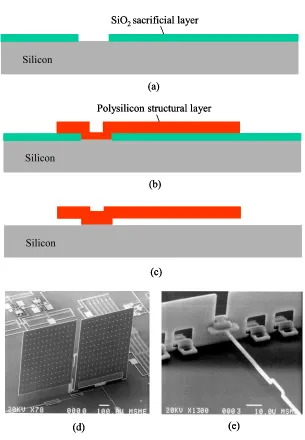
1.1.2.2 Surface Micromachining Technology
Surface micromachining technology is used for building micro structures on top
of the substrate. Structures are in general formed using multiple steps of thin-film
processes. The substrate only provides a mechanical support for the surface thin-film
structures and typically does not participate in the processing.
A typical surface micromachining process uses two types of thin-film materials:
structural and sacrificial materials. The structural materials can be polysilicon, SiO2, Si3N4, different types of polymers (parylene, PMMA, Teflon, etc.) or even metals. The sacrificial layers can be polysilicon, phosphosilicate glass (PSG), SiO2, polymers (photoresist and polyimide), or metals. In the beginning of the process, a sacrificial layer
is deposited and patterned on the substrate (Figure 1-3). The structural layer is then
deposited and patterned into desirable forms. Finally, the sacrificial layer is removed by
wet or dry etching to release the target structures. With multiple layers of different
structural materials deposited on top of each other, complicated devices of various
functionalities can be fabricated as shown in Figure 1-3(d,e).
1.1.2.3 Other Technologies
Besides bulk and surface micromachining there are numerous MEMS fabrication
technologies developed for specific applications. For example, LIGA (a German
acronym for Lithographie, Galvanoformung, Abformung) combines the molding method
with X-ray lithography and electroplating. The combination usage of electroplating and
X-ray lithography was first carried out at IBM in 1975 by Romankiw, et al. [14]. The
resist patterns of height up to 20 µm. This work was first done without the molding. The
addition of molding to the lithography and electroplating process was developed by W.
Ehrfeld, et al. [15]. The process is capable of yielding an extremely high-aspect-ratio structure (at least 100:1).
Silicon
(c)
(d) (e)
Silicon
SiO2 sacrificial layer
(a)
Silicon
Polysilicon structural layer
(b)
Silicon
(c)
(d) (e)
Silicon
(c) Silicon
(c)
(d) (e)
(d) (e)
Silicon
SiO2 sacrificial layer
(a)
Silicon
Polysilicon structural layer
(b) Silicon
SiO2 sacrificial layer
(a)
Silicon
Polysilicon structural layer
(b)
Figure 1-3: Surface micromachining technology, (a) deposition and patterning of SiO2 sacrificial layer, (b) deposition and patterning of polysilicon structural layer, (c)
Besides LIGA, some representative technologies include silicon-silicon fusion
bonding [16], silicon-glass anodic bonding [17], 3-D stereolithography [18], micro
electrical discharge machining (EDM) [19], laser micromachining [20], plastic injection
molding [21], etc.
1.1.2.4 Summary
MEMS fabrication technologies introduced above including bulk
micromachining, surface micromachining, and others can be combined in a single
process flow to make complicated micro structures to serve versatile application needs.
For example, Figure 1-4 shows a silicon-micromachined neurochip upon which cultured
mammalian neurons can be continuously and individually monitored and stimulated [22].
The neurochip is based upon a surface-micromachined 4x4 array of metal electrodes,
each of which has a bulk-micromachined well structure (created by EDP etch) designed
to hold a single mature cell body while permitting normal outgrowth of neural processes.
(a) (b)
20 µm
100 µm
Figure 1-4: Integrated surface/bulk micromachining technology. (a) SEM of a neurochip
cleaved to reveal the cross-section of a well. (b) Micrograph of a hippocampal culture on
1.1.3 Market and Products of MEMS Technology
In 1959, Richard Feynman gave his famous speech titled “There’s plenty of room
at the bottom,” at Caltech, in which he declared the tremendous application opportunities
in the miniaturization of machines [23]. In 1965, the first MEMS device, a resonant gate
transistor, was demonstrated [24]. In 1982, Kurt Peterson’s groundbreaking paper
“Silicon as a mechanical material,” [1] summarized many micromachining developments
to that date, which greatly increased the awareness of MEMS. In 1989, researchers at the
University of California Berkeley demonstrated the first IC-processed electrostatic
micro-motors [25, 26], after which a wide variety of MEMS devices, technologies, and
applications have been developed.
Over the past decade, various MEMS applications such as hard disk read/write
heads, ink-jet printer head, pressure sensors, and accelerometers have proven their values
in the marketplace. The fast-growing MEMS market and potential MEMS applications
have attracted more and more researchers and funding resources into this field which
effectively speeds up the commercialization of MEMS products. Table 1-2 lists some of
the main reasons why miniaturization presents opportunities for product innovation in
many application areas.
Figure 1-5 summarizes the results of 13 market studies published between 1990
and 2000 [28]. The wide disparity in totals comes from the different definitions of what
is considered to be MEMS in various studies. A broader, beyond silicon, definition of
products, which was used in the NEXUS report, results in the higher number of totals.
The silicon-based MEMS products are actually only a small part of the total projected
markets. According to the latest NEXUS market analysis for MEMS and Microsystems
published in 2005, the MEMS market will grow from $33 billion in 2004 to $57 billion in
2009 with a growth rate of 11% per year [29]. The main drive for the market growth
comes from the increasing consumer needs for read/write heads, micro displays and
inkjet heads. Figure 1-6 shows the market breakout for 1st-level-packaged MEMS and
MST products [29].
Table 1-2: Advantages of miniaturization technologies [27].
• Minimizing of energy and materials consumption during manufacturing • Redundancy and arrays
• Integration with electronics, simplifying systems • Increased sensor selectivity and sensitivity • Minimally invasive medical devices • Wider dynamic range
• Exploring new phenomena in the micro domain for applications • Improved accuracy and reliability
• Self-assembly and biomimetics with nanochemistry • More intelligent materials with structures at the nanoscale
It is important to note that while MEMS borrows fabrication technologies from
the IC world, it has a very different market character. The cost of ICs can be lowered
when the quantity of parts numbers in the millions per year. For silicon-based sensors to
succeed on the same scale as ICs, one must then concentrate on mass-consumption
products such as cars, air conditioners, toys, etc. However, about 50,000 types of sensors
exist to measure 100 different physical and chemical parameters, so often only 1,000 to
10,000 units are needed for each type of sensor per year. Therefore fragmentation
Figure 1-5: Various microsystems market studies from 1990 to 2000 [28].
sources
system Telecom
1.2 Lab-on-a-Chip
System by MEMS Technology
Over the past decade, MEMS has grown rapidly to cover a wide variety of
applications in many fields such as MOEMS (Micro-Optical-Electro-Mechanical
System), RF-MEMS, Bio-MEMS, and Lab-on-a-Chip System (LOC). Among all MEMS
applications, LOC is one of the most exciting and promising fields, which has attracted
tremendous research resources from industry and academia.
1.2.1 Applications of Lab-on-a-Chip System
The concept of lab-on-a-chip is the miniaturization and integration of the
complete functionality of a chemistry or biology lab, such as sample preparation,
reactions, separations, and detection, onto a single chip. The advantages of LOC
compared with its desktop counterparts are manyfold. For example, the system physical
size is significantly smaller and therefore of much higher portability. Power, sample,
reagent consumption and operational costs are greatly reduced [30]. Faster analysis is
achievable due to the significantly smaller system fluidic dead/swept volume. Also,
because of the large surface to volume ratio in microfluidics, analysis sensitivity and limit
of detection can be improved. Finally, the batch-fabrication of LOC using MEMS
technology effectively reduces manufacturing cost and accordingly the LOC systems are
highly disposable.
The birth date of the first LOC system can be traced back to 1979 when a
miniaturized gas chromatography system was demonstrated [31]. Today, LOC has
grown tremendously into a large, multidisciplinary field. The field is extensively
include proteomics and genomics research, high-throughput screening (HTS) of drug
candidates, point-of-care (POC) diagnostics, drug delivery, environment monitoring,
industrial online analysis, food safety, bio-defense, etc. Table 1-3 lists some of the
prominent LOC companies and their technologies/products [27].
Table 1-3: LOC companies [27].
Company Product
Aclara Biosciences
(Mountain View, CA) Plastic microfluidic chips (LabCard) for drug screening and genomic applications Agilent Technologies
(Palo Alto, CA)
Manufacturing and marketing instruments for Caliper Technologies’ LabChips
Amersham Pharmacia Biotech/Molecular Dynamics
(Piscataway, NJ)
Researching microchannel electrophoresis DNA sequencing devices
Applied Biosystems (Foster City, CA)
Collaborating with Aclara Biosciences to develop and market LabCard Systems
Caliper Technologies (Mountain View, CA)
Lab-on-chip devices, moving small volumes of liquids using electrical and pressure; applications include DNA and RNA analysis and protein separations
Cepheid
(Sunnyvale, CA)
DNA analysis systems based on microfluidics and microelectronics technology, emphasis on sample preparation and real time PCR
Tecan Boston (Medford, MA)
Lab-on-a-disc technology that uses centripetal force to move liquids; supporting a wide variety of bioanalytical applications
Burstein Technologies
(Irvine, CA) Lab-on-a-disk technology with emphasis on diagnostics Gyros
(Sweden)
Lab-on-a-disk technology that uses centripetal force to move liquids; supporting a wide variety of bioanalytical applications
Orchid Biosciences (Princeton, NJ)
Focusing on a microfluidic system for combinatorial drug synthesis
Micronics (Redmond, WA)
Microfluidics systems for diagnostics, analytical chemistry, and process applications
Nanogen
1.2.2 Challenges and Outlooks
While it is clear that LOC systems possess many advantages, producing a
commercial LOC system that can readily be used to replace a conventional chemical lab
or macro system is surely not an easy task. Some of the major challenges include: 1)
on-chip sample preparation, 2) world-to-on-chip interfacing, 3) on-on-chip optical detection, and 4)
on-chip components integration.
On-chip sample preparation turns out to be an extremely challenging task for all
LOC systems. Before any analysis, impurities in the raw sample (underground water, sea
water, blood, urine, saliva, etc.) need to be removed so that the target composition can be
appropriately processed and analyzed. Those impurities can be dirt particles, cells,
proteins, ions, or others. While this sample purification task might be straightforward for
manual processing in a conventional chemical lab, it is extremely difficult to carry out on
LOC systems. Different impurities require different procedures and facilities to remove
and therefore sample preparation needs to be handled on a case by case basis. Trace level
impurities that stays with the sample might interfere the sensing of sample species and
jeopardize the quantification accuracy and reproducibility. Two reviews on sample
preparation in microfluidic systems are given in [35, 36].
Let’s assume that raw samples are processed off-chip by conventional procedures
and are ready for analysis, the next problem is to deliver/couple the processed samples,
reagents, and conventional macro-scale tubing to the LOC system. This procedure is
often referred to as “world-to-chip interfacing,” which remains a challenging issue for
LOC. For example, the sample volume processed in the LOC system can be as small as 1
LOC system using the macro tubing and pumps where a fluidic swept/dead volume of a
few µL can be easily found. Also, in the case of high pressure LOC applications such as
liquid chromatography, world-to-chip interfacing needs to withstand operational pressure
as high as 1,000 psi without leaking or fracture. Any fluidic leak rate larger than 10
nL/min can significantly degrade the overall LOC performance. Therefore, robust and
small-swept-volume world-to-chip interfacing technology needs to be developed [37].
Optical detection such as UV absorption and laser-induced fluorescence detection
are frequently used sensing tools in chemistry and biology for a broad range of analytes.
The limit of detection (LOD) of optical detection is defined by the minimum sensible
amount of photons that are collected by the photo detector per unit time. For the
microfluidic system, since the sample volume is much smaller than the macrofluidic
system, it can be expected that its lowest sensible analyte concentration will be much
higher than that of macrofluidic system. To compensate for this drawback, techniques to
increase on-chip optical path or analyte concentration need to be developed. Furthermore,
many of today’s optical detection setups for LOC are still using off-chip light sources and
detectors. This introduces complexities in optical alignments between the on-chip
microfluidic cell and off-chip optical components. To avoid the alignment issue, light
source and detectors need to be fabricated on the chip, which can be quite challenging as
well.
Finally, most of the developments in LOC so far have been focused on discrete
devices, such as channels, valves, pumps, flow sensors, pressure sensors, and
electrochemical sensors, etc. To realize a complete LOC concept, however, all necessary
chip. It is understandable that the more components to be integrated on a chip the more
difficult and likely lower-yield the process will be. Well, the multichip module (MCM)
approach [38] is surely an alternative to be used for complicated systems. The major
advantage of it is that the fabrication process for each chip will be much simpler and each
component of the system can be designed or replaced individually with maximum
flexibility. However, the MCM approach also introduces complexities such as
microfluidic coupling between chips. A major goal of this thesis is to demonstrate with
real examples (microchip HPLC systems) that reliable MEMS processes can be designed
to achieve extensive components integration for LOC applications.
1.3 Parylene as a Microstructure Material
1.3.1 Introduction to Parylene
Parylene (poly-para-xylylene) was discovered in 1947 and commercialized by
Union Carbide Corporation in 1965. Parylene has been used in several industries because
of its unique properties. One of its primary applications is PCB (printed circuit board)
coating for the electronics industry, where parylene coating isolates the delicate
electronic devices from moisture and corrosive environments. Figure 1-7 shows the
chemical structures of the three most frequently used parylene types: parylene N,
parylene C, and parylene D.
CH2 CH2
Cl
n
CH2 CH2
Cl
n
Parylene C
CH2 CH2
Cl
n Cl
CH2 CH2
Cl
n Cl
Parylene D
CH2 CH2
n
CH2 CH2
n
Parylene N
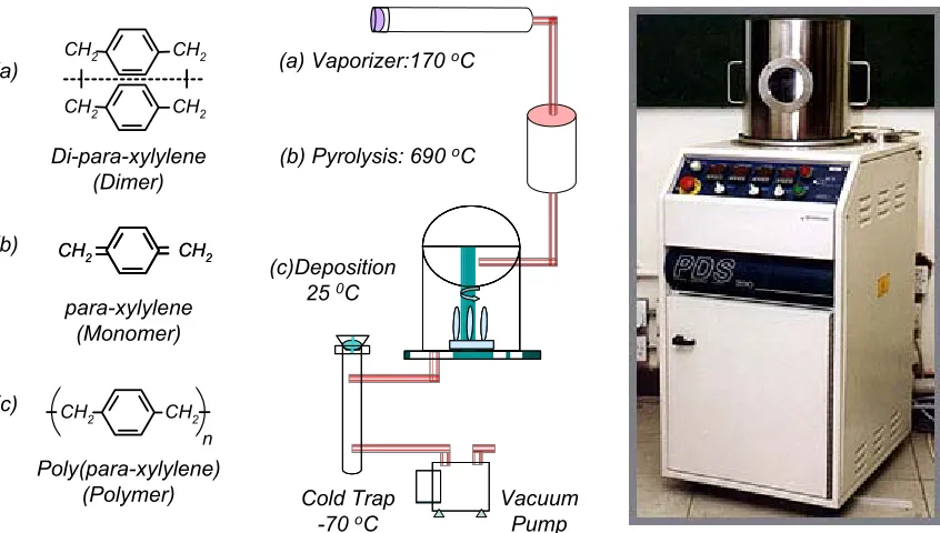
Figure 1-8 shows the parylene deposition procedures, the involved chemical
processes, and the instrument. The process starts with placing parylene dimer
(di-para-xylylene), a stable compound in granular form, into the vaporizer. The substrate to be
coated with parylene is put into the deposition chamber. The whole system is then
pumped down to medium vacuum (8-10 mTorr). The dimer is heated in the vaporizer
and sublimed into vapor at around 170 °C. The dimer vapor enters the pyrolysis furnace
that is maintained at 690 °C, where the dimers are cleaved into identical monomers
(para-xylylene). In the room-temperature deposition chamber, the monomers reunite on all
exposed surfaces in the form of polymers (poly-para-xylylene). Deposition chamber
pressure is around 23 mTorr. Additional components of the system include a mechanical
vacuum pump and associated cold trap to take away extra monomer vapor. Although
parylene N structure is used in Figure 1-8, the deposition process is almost identical for
all three common types of parylene, except for some slight differences in pyrolysis
temperature and deposition pressure.
Typical parylene coating thickness in a single deposition run ranges from 0.1 to
20 microns. Sub-micron parylene deposition is trickier because thickness uniformity can
be a concern. In general, the coating thickness is in proportion to the amount of dimer
used. Chamber condition including cleanness, base pressure, and temperature fluctuation
can result in a slight deposition rate change. The normal deposition rate of parylene C
under a deposition vapor pressure of 23 mTorr is about 5 µm per hour. The deposition
rate is directly proportional to the square of the monomer concentration in the chamber
and inversely proportional to the absolute temperature of the substrate on which parylene
CH2 CH2 n
Di-para-xylylene (Dimer)
para-xylylene (Monomer)
Poly(para-xylylene) (Polymer)
CH2 CH2
CH2 CH2
CH2 CH2
CH2 CH2
(a)
(c) (b)
(a) Vaporizer:170oC
(b) Pyrolysis: 690oC
(c)Deposition 25 0C
Cold Trap -70oC
Vacuum Pump
Figure 1-8: Parylene deposition system and the involved chemical processes.
Since parylene thin film is deposited using chemical vapor deposition (CVD), the
deposited film is highly conformal. As mentioned earlier, parylene is an excellent barrier
to gas and moisture. Compared with PDMS (polydimethylsiloxane), which is another
popular material for microfluidic devices, the gas permeability of parylene is more than
four orders of magnitude smaller and moisture permeability is ten times smaller.
Parylene is extremely inert to most chemicals and solvents used in chemical or biological
laboratories. Manufacturer’s study [40] shows that solvents have a minor swelling effect
on parylene N, C, and D with a 3% maximum increase in film thickness. The swelling is
completely reversible after the solvents are removed from parylene by vacuum drying.
Furthermore, parylene is biocompatible (USP Class VI), which makes it a good candidate
As for mechanical properties, parylene has an elongation break of 200%. This
mechanical flexibility makes it a durable material for composing MEMS microfluidic and
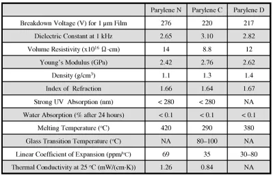
actuation devices. Parylene is also an excellent electrical and thermal insulator. The
electrical breakdown voltage of a 1-µm-thick parylene layer is over 200 volts. The room
temperature thermal conductivity of parylene C (0.84 mW/cm-K) is only three times as
big as static air (0.30 mW/cm-K). In terms of optical properties, parylene is pretty much
transparent in the visible light range. However, parylene begins to absorb light with
wavelength shorter than 280 nm significantly, which limits some of its UV applications.
The difference in chemical structures between parylene N, C, and D as shown in
Figure 1-7 actually results in different thin-film properties. For example, parylene N has
the lowest gas/moisture permeability. However, parylene N also has the lowest
deposition rate which is not favorable in a mass production process. In terms of choosing
a micromachining material from the three parylene species, parylene C has a good
combination of electrical and physical properties plus a low permeability to moisture and
other corrosive gases. Parylene C also has higher deposition rate than parylene N, and D.
Therefore, parylene C is often chosen to fabricate microstructures. In our lab, parylene C
was chosen 99% of the time to build devices and the deposition parameters have been
well characterized so to guarantee good thin film qualities which include film
transparency, thickness uniformity/accuracy, and adhesion properties to assorted
substrates. Parylene C was as well used exclusively in this thesis to build devices.
Detailed electrical, mechanical, thermal, optical, and other properties can be
found on a parylene vendor’s website [39]. A list of selected properties for parylene N, C,
Table 1-4: Properties for parylene N, C, and D.
1.3.2 Applications of Parylene Thin Film in MEMS
As mentioned in the previous section, parylene thin film is deposited using a room
temperature CVD process that makes parylene deposition a post-CMOS compatible
process. Besides, parylene thin film can be easily patterned using a conventional
lithography process plus oxygen plasma etching (with photoresist or metal as the mask).
Combining with other MEMS surface micromachining technologies introduced earlier,
one can build assorted microstructures using parylene as the structural material. The
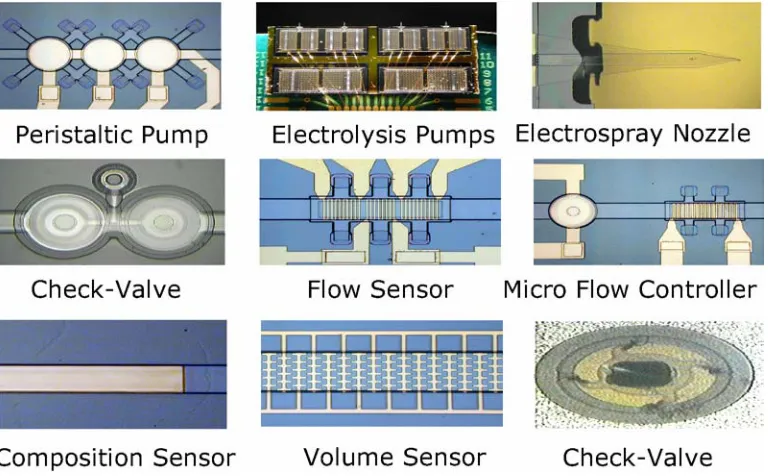
conformal coating characteristics of parylene and its mechanical robustness make it a
favorable structural material and technology in microfluidics. Parylene microfluidic
devices such as channels, pumps, valves, filters, pressure and flow sensors, mass flow
controllers, electrospray nozzles, and gas chromatography columns have been
parylene technology provides a straightforward process solution for integrating various
microfluidic components on a single chip. Moreover, the bio-compatibility of parylene
makes it a perfect material for building biological sensing or implantable devices [47].
Figure 1-9: Parylene microfluidic devices.
In this thesis, parylene technology is explored thoroughly to build MEMS
lab-on-a-chip high-performance liquid chromatography (HPLC) system. Parylene technology is
chosen here mainly due to its great chemical resistance, mechanical robustness, optical
transparency, and its ease of process integration, which are all crucial factors in making a
1.4 Bibliography
[1] K. E. Petersen, "Silicon as a mechanical material," Proceedings of the IEEE, vol.
70, pp. 420-457, 1982.
[2] G. T. A. Kovacs, N. I. Maluf, and K. E. Petersen, "Bulk micromachining of
silicon," Proceedings of the IEEE, vol. 86, pp. 1536-1551, 1998.
[3] H. Robbins and B. Schwartz, "Chemical Etching of Silicon 2. The System HF,
HNO3, H2O, and CH3COOH," Journal of the Electrochemical Society, vol. 107, pp. 108-111, 1960.
[4] H. F. Winters and J. W. Coburn, "Etching of Silicon with XeF2 Vapor," Applied Physics Letters, vol. 34, pp. 70-73, 1979.
[5] D. E. Ibbotson, J. A. Mucha, D. L. Flamm, and J. M. Cook, "Plasmaless Dry
Etching of Silicon with Fluorine-Containing Compounds," Journal of Applied
Physics, vol. 56, pp. 2939-2942, 1984.
[6] X. Q. Wang, X. Yang, K. Walsh, and Y. C. Tai, "Gas phase silicon etching with
bromine trifluoride," presented at 9th International Conference on Solid-State
Sensors and Actuators (Transducers '97), Chicago, USA, 1997.
[7] C. Y. Shih, T. A. Harder, and Y. C. Tai, "Yield strength of thin-film parylene-C,"
Microsystem Technologies, vol. 10, pp. 407-411, 2004.
[8] T. J. Yao, X. Yang, and Y. C. Tai, "BrF3 dry release technology for large freestanding parylene microstructures and electrostatic actuators," Sensors and
Actuators a-Physical, vol. 97-8, pp. 771-775, 2002.
[9] K. E. Bean, "Anisotropic Etching of Silicon," IEEE Transactions on Electron
[10] K. R. Williams and R. S. Muller, "Etch rates for micromachining processing,"
Journal of Microelectromechanical Systems, vol. 5, pp. 256-269, 1996.
[11] U. Schnakenberg, W. Benecke, and B. Lochel, "Nh4Oh-Based Etchants for
Silicon Micromachining," Sensors and Actuators A-Physical, vol. 23, pp.
1031-1035, 1990.
[12] S. A. McAuley, H. Ashraf, L. Atabo, A. Chambers, S. Hall, J. Hopkins, and G.
Nicholls, "Silicon micromachining using a high-density plasma source," Journal
of Physics D-Applied Physics, vol. 34, pp. 2769-2774, 2001.
[13] M. Last and K. Pister, "2DOF actuated micromirror designed for large DC
deflection," presented at the 3rd International Conference on Micro Opto Electro
Mechanical Systems (MOEMS '99), Mainz, Germany, 1999.
[14] E. Spiller, R. Feder, J. Topalian, E. Castellani, L. Romankiw, and M. Heritage,
"X-Ray Lithography for Bubble-Devices," Solid State Technology, vol. 19, pp.
62, 1976.
[15] E. W. Becker, W. Ehrfeld, D. Munchmeyer, H. Betz, A. Heuberger, S. Pongratz,
W. Glashauser, H. J. Michel, and R. Vonsiemens, "Production of
Separation-Nozzle Systems for Uranium Enrichment by a Combination of X-Ray
Lithography and Galvanoplastics," Naturwissenschaften, vol. 69, pp. 520-523,
1982.
[16] M. Shimbo, K. Furukawa, K. Fukuda, and K. Tanzawa, "Silicon-to-Silicon Direct
Bonding Method," Journal of Applied Physics, vol. 60, pp. 2987-2989, 1986.
[17] T. R. Anthony, "Anodic Bonding of Imperfect Surfaces," Journal of Applied
[18] J. Brook and R. Dandliker, "Submicrometer Holographic Photolithography," Solid
State Technology, vol. 32, pp. 91-94, 1989. [19] E. B. Guitrau, The EDM Handbook, 1997.
[20] R. Srinivasan and V. Maynebanton, "Self-Developing Photoetching of
Poly(Ethylene-Terephthalate) Films by Far Ultraviolet Excimer Laser-Radiation,"
Applied Physics Letters, vol. 41, pp. 576-578, 1982.
[21] P. Hagmann, W. Ehrfeld, and H. Vollmer, "Fabrication of microstructures with
extreme structural heights by reaction injection molding," presented at the 1st
Meeting of the European Polymer Federation, European Symposium on
Polymeric Materials, Lyon, France, 1987.
[22] M. P. Maher, J. Pine, J. Wright, and Y. C. Tai, "The neurochip: a new
multielectrode device for stimulating and recording from cultured neurons,"
Journal of Neuroscience Methods, vol. 87, pp. 45-56, 1999.
[23] R. P. Feynman, "There's plenty of room at the bottom," Journal of
Microelectromechanical Systems, vol. 1, pp. 60-66, 1992.
[24] H. C. Nathanson, W. E. Newell, R. A. Wickstrom, and J. J. R. Davis, "The
resonant gate transistor," IEEE Trans. Electron Devices, vol. 14, pp. 117- 133,
1967.
[25] L.-S. Fan, Y.-C. Tai, and R. S. Muller, "IC-processed electrostatic micromotors,"
Sensors and Actuators, vol. 20, pp. 41-47, 1989.
[26] Y.-C. Tai and R. S. Muller, "IC-processed electrostatic synchronous
[27] M. J. Madou, Fundamentals of Microfabrication, 2nd ed. New York: CRC Press,
2002.
[28] Editors, "Market forecast sees 25% CAGr in MST in 2004," Micromachine
Devices, vol. 5, pp. 12, 2000.
[29] NEXUS, "NEXUS market analysis for MEMS and Microsystems III, 2005-2009,"
2005.
[30] J. Xie, Y. N. Miao, J. Shih, Q. He, J. Liu, Y. C. Tai, and T. D. Lee, "An
electrochemical pumping system for on-chip gradient generation," Analytical
Chemistry, vol. 76, pp. 3756-3763, 2004.
[31] S. C. Terry, J. H. Jerman, and J. B. Angell, "Gas-Chromatographic Air Analyzer
Fabricated on a Silicon-Wafer," IEEE Transactions on Electron Devices, vol. 26,
pp. 1880-1886, 1979.
[32] D. R. Reyes, D. Iossifidis, P. A. Auroux, and A. Manz, "Micro total analysis
systems. 1. Introduction, theory, and technology," Analytical Chemistry, vol. 74,
pp. 2623-2636, 2002.
[33] P. A. Auroux, D. Iossifidis, D. R. Reyes, and A. Manz, "Micro total analysis
systems. 2. Analytical standard operations and applications," Analytical
Chemistry, vol. 74, pp. 2637-2652, 2002.
[34] T. Vilkner, D. Janasek, and A. Manz, "Micro Total Analysis Systems. Recent
Developments," Analytical Chemistry, vol. 76, pp. 3373-3386, 2004.
[35] A. J. de Mello and N. Beard, "Dealing with 'real' samples: sample pre-treatment in
[36] J. Lichtenberg, N. F. de Rooij, and E. Verpoorte, "Sample pretreatment on
microfabricated devices," Talanta, vol. 56, pp. 233-266, 2002.
[37] Q. He, C. Pang, Y. C. Tai, and T. D. Lee, "Ion liquid chromatography on-a-chip
with beads-packed parylene column," presented at the 17th IEEE International
Conference on MicroElectroMechanical Systems (MEMS 2004), Maastricht, The
Netherlands, 2004.
[38] S. Linder, H. Baltes, F. Gnaedinger, and E. Doering, "Fabrication technology for
wafer through-hole interconnections and three-dimensional stacks of chips and
wafers," presented at the 7th IEEE International Conference on Micro Electro
Mechanical Systems (MEMS 1994), Oiso, Japan, 1994.
[39] http://www.scscookson.com/parylene_knowledge/specifications.cfm
[40] Specialty Coating Systems, "Solvent resistance of the parylene." Trade literature.
[41] L. Licklider, X. Q. Wang, A. Desai, Y. C. Tai, and T. D. Lee, "A micromachined
chip-based electrospray source for mass spectrometry," Analytical Chemistry, vol.
72, pp. 367-375, 2000.
[42] J. Xie, Y. Miao, J. Shih, Q. He, J. Liu, Y. C. Tai, and T. D. Lee, "An
Electrochemical Pumping System for On-Chip Gradient Generation," Analytical
Chemistry, vol. 76, pp. 3756-3763, 2004.
[43] H. S. Noh, P. J. Hesketh, and G. C. Frye-Mason, "Parylene gas chromatographic
column for rapid thermal cycling," Journal of Microelectromechanical Systems,
[44] X. Q. Wang and Y. C. Tai, "Normally closed in-channel micro check valve,"
presented at the 13th IEEE International Conference on Micro Electro Mechanical
Systems (MEMS 2000), Miyazaki, Japan, 2000.
[45] J. Xie, X. Yang, X. Q. Wang, and Y. C. Tai, "Surface micromachined leakage
proof parylene check valve," presented at the 14th IEEE International Conference
on Micro Electro Mechanical Systems (MEMS 2001), Interlaken, Switzerland,
2001.
[46] J. Xie, J. Shih, and Y. C. Tai, "Integrated surface-micromachined mass flow
controller," presented at the 16th IEEE International Conference on Micro Electro
Mechanical Systems (MEMS 2003), Kyoto, Japan, 2003.
[47] D. C. Rodger and Y. C. Tai, "Microelectronic packaging for retinal prostheses,"
C
HAPTER
2
EVOLUTION of HPLC TECHNOLOGY
2.1 High-Performance Liquid Chromatography
2.1.1 Introduction
High-Performance Liquid Chromatography (HPLC) is one of the most powerful
analysis tools widely used in fields such as the pharmaceutical industry, food industry,
chemistry, biology, forensic analysis, and clinical analysis. HPLC provides separation,
identification, purification, and quantification of chemical compounds such as proteins,
peptides, ions, polymers, and amino acids as long as samples can be prepared in the
solution format.
Chromatography in general includes all separation techniques in which analytes
partition between different phases that move relative to each other. In most
chromatographic techniques, one phase is stationary and the other phase is mobile. If the
Chromatography (LC). The LC stationary phase is solid or porous with a specific surface
property. The surface property of the stationary phase can be adjusted by bonding
molecules with desirable chemical functional groups to its surface. HPLC means LC
techniques that use a packed bed of stationary phase composed of particles with
dimensions smaller than 10 µm. The small particle size creates a large stationary-phase
surface which dramatically enhances the chromatography efficiency. The densely packed
HPLC column also requires an elevated backpressure to push the mobile phase forward
and therefore HPLC is also called high-pressure liquid chromatography.
The chromatography procedures start with sample injection to the separation
column. Sample molecules adsorb to the stationary phase in the beginning section of the
column and form a narrow sample band. The mobile phase is then injected to elute
sample molecules out of the column. Due to the fact that different sample molecules
have different adsorption strengths to the stationary phase, molecules will migrate in the
column with different speeds and exit the column at different times. A sensor located at
the outlet of the separation column is used to quantitatively sense the eluted sample peaks
and the output data of the sensor is used to plot chromatograms. This process is
illustrated in Figure 2-1.
If the mobile phase chemical composition is constant throughout the elution, the
elution process is called isocratic elution. Obviously, isocratic elution is most
straightforward to carry out compared with other elution strategies where mobile phase
conditions change throughout the elution process. However, when a sample mixture
contains tens of compounds or more, isocratic elution can be problematic. Early peaks
can crowd together with poor peak resolution and late peaks are broad in shape and can
take a long time to elute. Using a mobile phase with weaker elution strength can improve
early peaks resolution since elution time of each peak will be longer and so are the
differences of elution times among peaks. Using a mobile phase with stronger elution
strength, on the other hand, can shorten the elution times of the late peaks. Therefore, by
starting the elution with a weak mobile phase and gradually increasing the mobile-phase
elution strength over the separation process, the chromatography performance can be
significantly improved. This elution strategy is called gradient elution. Depending on
the elution mechanisms, a gradient elution can be generated by changing the mobile
phase parameters such as salt concentration, water/organic solvent ratio, temperature or,
pH values over time.
2.1.2 History
The discovery of liquid chromatography can be traced back to 1903 when the
Russian botanist Mikhail Twsett (1872-1919) observed that colored plant pigments could
be separated on a chalk column where ether was run through as the mobile phase (Figure
2-2) [1]. The separation of pigments appeared as colored bands on the column, which
Figure 2-2: The inventor of chromatography, Twsett, and his chromatographic device.
In 1941, Martin and Synge developed the theoretical background for partition
chromatography and used mathematical formulae to describe the separation process [2],
for which they were awarded the Nobel Prize in chemistry (1952). The development of
the open-column chromatography in the 1940s and thin-layer chromatography in the
1950s greatly improved the speed and resolution of LC, but there were still serious
limitations compared to modern LC methods in terms of resolution and quantitative
analysis capability. By the late 1960s, LC theories and instrumentation were
well-established, which led to the first commercially available liquid chromatography system
in 1969. In 1973, due to the advances in stationary phase fabrication and packing
technologies, high-efficiency columns could be prepared with particle diameters smaller
than 10 µm and reproducible separations were achievable. In the same year, modification
of silica surfaces via silanization became commercially available. These breakthroughs
led to the birth of the first commercial 10 µm reversed-phase HPLC column [3]. Since
then, HPLC has grown to become one of the most important analytical tools in
2.1.3 Theory
2.1.3.1 Analyte Retention and Chromatogram
Each peak in a chromatogram represents the elution of an analyte species.
According to the theory [4], an ideal peak should have a Gaussian curve. The height and
area of a peak are proportional to the concentration and total number of molecules of that
analyte species in the injected sample, respectively.
The retention time of a peak tR is defined as the time length from the beginning of
sample injection to the time that peak maximum occurs in the chromatogram as shown in
Figure 2-3. The breakthrough time t0 is defined as the time that the mobile phase takes to
travel through the column. If the column length is Lc and the mobile phase linear flow
velocity is u, then:
0 c
L t
u
= (2.1)
Analyte 1
Analyte 2
The mobile phase volumetric flow rate F is:
c
F =εuA (2.2)
where Ac is the column cross-sectional area and ε is the column porosity. For cylindrical
columns with an inner diameter (ID) of dc:
2
4
c c
d A =π
(2.3)
The column porosity ε is:
column packing
column
V V
V
ε = − (2.4)
where Vcolumn is the total volume inside the column and Vpacking is the volume occupied by
the solid packing material in the column.
As shown in Figure 2-3, '
R
t is the net/adjusted retention time relative to t0:
'
0
R R
t = −t t (2.5)
0
t , as defined earlier, also represents the time an analyte spends in the mobile phase,
which is identical for all analytes assuming all analytes move at speed u when they are in
the mobile phase. '
R
t represents the time an analyte spends in the stationary phase. The
longer an analyte stays in the stationary phase, the later it will be eluted. Ideally, any two
analytes can be separated and resolved from each other using liquid chromatography
techniques as long as their retention times are different and if the separation column is
long enough.
The retention factor k of an analyte is defined as:
'
0
0 0
R R t t t
k
t t
−
To characterize an analyte, the retention factor k is preferred over the retention time,
because the retention time depends on column length and mobile-phase flow velocity
while retention factor does not. The retention factor is the ratio of the time that an
analyte spends in the stationary phase to the time it spends in the mobile phase, which is
also the ratio of the number of analyte molecules that are at any time in/on the stationary
phase NS to the number of analyte molecules that are in the mobile phase NM:
S M N k
N
= (2.7)
This equation enables us to make the link between the retention factor of an analyte and
the thermodynamics of the separation, which will be discussed as follows.
From equation (2.7), we can relate the numbers of molecules in the stationary
phase and in the mobile phase to their respective concentrations cM and cS:
=
S S S M M M N c V k
N c V
= (2.8)
where VM and VS are the volumes of the mobile phase and stationary phase, respectively.
Their ratio is called the phase ratio ß:
S M V V
β ≡ (2.9)
The ratio of the concentrations cS and cM is the partition coefficient K:
S M c K
c
≡ (2.10)
Therefore the retention factor is the product of the phase ratio and the partition
coefficient:
We also know the relationship between the partition coefficient (equilibrium constant)
and the standard Gibbs free-energy change DG0 associated with this chemical equilibrium
(DG=0):
0 ln
G RT K
∆ = − (2.12)
Therefore, by combining (2.11) and (2.12), the logarithm of the retention factor is a
function of the free energy [5]:
0 0 0
lnk G ln H S ln
RT β RT R β
∆ ∆ ∆
= − + = − + + (2.13)
where DH0 and DS0 are the standard enthalpy and entropy changes associated with the
transfer of the analyte molecules from the mobile phase to the stationary phase, R is the
gas constant, and T is the absolute temperature.
The relative retention a is defined as the ratio of the retention factors of two
analytes:
2 2
1 1
k K k K
α ≡ = (2.14)
The retention factor of the later-eluting analyte is in the numerator, making the value
always larger than one. The relative retention is purely a chemical or thermodynamic
entity that does not depend on the physical parameters of the column anymore. One can
use it to verify whether the chemistry of a separation remains invariant when transferring
the separation from one column to another.
Now we discuss the definition of chromatography peak resolution RS. As shown
in Figure 2-3, w is the peak width. When measured at 13.4% of the height of a Gaussian
two peaks is defined as the ratio of the two-peak maxima distance to the mean of the two
peak widths:
2 1
1 2
1
( )
2
R R S
t t R
w w
− ≡
⋅ +
(2.15)
Even though in (2.15) the peak resolution is defined and calculated in the time domain,
the peak resolution can as well be defined and calculated in the space domain. In that
case, resolution is the ratio of the two-peak maxima distance measured in length units to
the mean of the peak widths measured in length units. In reality, the distance between the
maximums of two peaks increases with the length that they have migrated in the column
while the widths of the peaks increase only with the square root of this length. Therefore,
chromatographic resolution increases with the square root of the distance traveled by the
peaks [4].
2.1.3.2 Height Equivalent to a Theoretical Plate
The height equivalent to a theoretical plate (HETP), H, can be treated as the
distance over which a chromatographic equilibrium cycle is achieved. The smaller the H
value, the higher the column efficiency.
As mentioned earlier, chromatographic band (peak) width is proportional to its
Gaussian distribution standard deviation σ . Because σ (in space domain) increases
with the square root of the length a peak has traveled in the column, L, the peak variance
2
σ increases linearly with the length it has traveled. The smaller the slope of σ2 vs. L
words, one can use shorter column length to achieve complete separation of two peaks.
The slope mentioned above (variance per unit length) is defined to be the HETP or H:
2
H L
σ
≡ (2.16)
The number of theoretical plates (or plate count) N is calculated by dividing the
column length Lc by H :
2
2
c c c L L N
H σ
≡ = (2.17)
where sc is the peak standard deviation (in space domain) at the end of the column. In
practice, plate count N can be calculated conveniently from the chromatogram:
2
16
( )
tR Nw
= (2.18)
The plate count N is a measure of the quality of a separation that is based on a
single peak. The plate count obtained from a non-retained peak is a measure of the
column packing efficiency. From (2.17) it is clear that higherN or higher separation
capability can be obtained using a longer column or reducing the peak variance.
Approaches to reduce peak variance or the band-broadening effect will be discussed in
2.1.3.4.
2.1.3.3 Reduced/Dimensionless Parameters
The concepts of reduced/dimensionless parameters such as reduced plate height or
reduced velocity are powerful ideas that allow us to compare columns to each other under
a broad range of mobile-phase conditions and over a range of stationary-phase particle
p
H h
d
≡ (2.19)
where dp is the stationary-phase particle diameter. h represents the number of layers of
stationary-phase particle packing over which a complete chromatographic equilibrium
cycle is obtained. A column with good stationary-phase packing usually has an h value
from 2 to 5. The reduced velocity v is defined as:
p
M ud v
D
≡ (2.20)
where DM is the analyte diffusion coefficient in the mobile phase.
One of the most frequently used reduced/dimensionless parameters is the
dimensionless flow resistance Ф, which is used to replace permeability:
2
p c Pd L uη
∆
Φ ≡ (2.21)
where ∆P is the pressure drop across the column length, η is the mobile phase viscosity.
Φ is between 500 (spherical beads) and 1,000 (irregular beads) for slurry-packed
columns containing totally porous particles and about 300 if non-porous particles are
used [6]. A much greater value of Φ (say 5,000) indicates a blockage somewhere in the
flow path. This equation can also be rearranged to estimate column backpressure:
2 c p L u P d η Φ
∆ = (2.22)
2.1.3.4 Band-Broadening Phenomenon
All chromatographic bands or peaks will continue to broaden as the bands move
a larger plate height and or lower column separation efficiency. Therefore, it is important <
![Figure 1-6: Market breakout for 1st-level-packaged MEMS and MST products [29].](https://thumb-us.123doks.com/thumbv2/123dok_us/1131193.1141780/29.612.157.490.68.404/figure-market-breakout-level-packaged-mems-mst-products.webp)
![Figure 2-3: Chromatogram and its characteristic features [4].](https://thumb-us.123doks.com/thumbv2/123dok_us/1131193.1141780/50.612.132.523.368.683/figure-chromatogram-characteristic-features.webp)