Available online: https://edupediapublications.org/journals/index.php/IJR/ P a g e | 2293
Design and Implementation of Novel Area Efficient
Scan Based Lbist
Using Lp Lfsr
B.Gayatri Devi
1M.Saritha Devi
2[email protected]
1[email protected]
21
PG SCHOLAR, VLSI&ES, Godavari Institute of Engineering and Technology (Rajahmundry)
2Assistant Professor, Department of ECE, Godavari Institute of Engineering and Technology
(Rajahmundry)
Abstract: Testing is a fundamental step in Very-Large-Scale Integration (VLSI) design. There are two major steps in VLSI testing. They are Test Generation (TG) and Test Application (TA) . The objective of TG is to produce test patterns for adequate testing and TA is the process of applying those test patterns to the CUT and analyzing the output response. The whole process is performed by LBIST. To handle the increasing complexity of testing VLSI circuits is to incorporate Logic Built-In Self Test (LBIST) structures. However, LBIST architecture calls for increased area overhead. It is very important to keep this area overhead to a minimum. And by applying test vectors Power Droop (PD) may appear in LBIST which will generate a delay affect on the circuit under test (CUT) and it is recognized as a fault. So In this paper, we designed a novel area efficient scan-based LBIST, and it is achieved by using the LP-LFSR and also by proper modification of test vectors. As a result, 72.5% of area and power droop (pd) of proposed system is diminished than the existing method and by SA high fault coverage is also achieved. The proposed design architecture has been coded in VERILOG HDL and the software used is Xilinx 13.2.
Index Terms—Testing, VLSI, LP LFSR, Power droop(PD), LBIST, CUT, Test Generation, Test Application, SA.
I. INTRODUCTION
LBIST stands for Logic Built-In-Self-Test. It is achieving importance by providing self-test capability to logic thus, the chip can test itself without any external equipment and also by finding the faults in a circuit design reduces the difficulty in VLSI testing. Now-a-days logic blocks at-speed test are performed by using Logic BIST (LBIST), which can take the form of either combinational LBIST or scan-based LBIST. It
depends on the CUT which is either a combinational circuit or a sequential one with scan.
There are two basic capture-clocking schemes in scan based LBIST. They are: 1) the skewed-load (also called as launch-on-shift (LOS)) scheme and 2) the board-side (also called as launch-on-capture (LOC)) scheme.
In skewed-load schemes, Test Vectors (TV) are applied to the CUT at the prior clock of the shift phase, and the CUT response is sampled on the scan chains at the following capture.
In the board-side scheme, first, the TV are first loaded into the scan chains(SC) during the shift phase; then, in a following capture phase, they are applied to the CUT at a launch, and the CUT response is captured on the scan chains in a following capture . Here in this paper, sequential CUTs with scan-based LBIST adopting an board-side scheme, which is frequently adopted for high speed performance microprocessors.
The increase in area and power droop (PD) are serious concerns for ICs’ testing. Excessive power droop (PD) will lead to IC fail, due to the abrupt changes in circuit activity (CA). So there is need to reduce the excessive pd and area.
In the literature, several solutions have been proposed to reduce PD, for combinational LBIST, while fewer approaches exist for scan-based LBIST. These techniques require very high area.
In this paper, TG is done by using LP-LFSR which produces the modified test vectors to minimize the circuit activity and only one of the flip-flops in the LFSR register is enabled during each shift operation to reduce the switching activities of the CUT and consumes less area as compared to the normal LFSR.
Available online: https://edupediapublications.org/journals/index.php/IJR/ P a g e | 2294
Existing Method, In Section IV Proposed Work, V
results are shown finally, some conclusions are drawn in Section VI.
II. LITERATURE SURVEY
Y. Sato, S. Wang, T. Kato, K. Miyase, and S. Kajihara, “Low power BIST for scan-shift and capture power”, Nov. 2012[2],proposed a Low-power test technology which has been investigated deeply to achieve an accurate and efficient testing. Although many sophisticated methods are proposed for scan-test, there are not so many for logic BIST because of its uncontrollable randomness. However, logic BIST currently becomes vital for system debug or field test. This paper proposes a novel low power BIST technology that reduces shift-power by eliminating the specified high-frequency parts of vectors and also reduces capture power. The authors show that the proposed technology not only reduces test power but also keeps test coverage with little loss.
N. Z. Basturkmen, S. M. Reddy, and I. Pomeranz, “A low power pseudorandom BIST technique,” Jul. 2002[9] , presents a pseudo-random BIST scheme for scan designs, which reduces the peak power consumption as well as the average power consumption as measured by the switching activity in the circuit. The method reduces the switching activity in the scan chains and the activity in the circuit under test by limiting the scan shifts to a portion of the scan chain structure using scan chain disable. Experimental results on various benchmark circuits demonstrate that the technique reduces the switching activity caused by scan shifts.. For scan designs, a high level of switching activity is created in the circuit during scan shifts, which increases power consumption considerably. The authors show the experimental results on various benchmark circuits demonstrate that the technique reduces the switching activity caused by scan shifts.
J. Rajski, J. Tyszer, G. Mrugalski, and B. Nadeau-Dostie, “Test generator with preselected toggling for low power built-in self-test,” in Proc. Eur. Test
Symp., May 2012[21], This paper presents a new
pseudorandom test pattern generator with preselected toggling (PRESTO) activity. It is comprised of a linear finite state machine (a linear feedback shift register or a ring generator) driving an appropriate phase shifter and armed with a number of features that allows this device to produce binary sequences with low toggling (switching) rates while preserving test coverage achievable by the best-to-date conventional BIST-based PRPGs with negligible impact on test application time.
III.
EXISTING SYSTEM
We adapted the widely used scan-based LBIST architecture presented in Fig.1. The state flip-flops of the CUT are converted into scan flip-flops, and arranged into many short scan chains (scan chains in Fig. 1).
Fig.1.Block Diagram of the adapted Scan Based Logic BIST architecture.
Available online: https://edupediapublications.org/journals/index.php/IJR/ P a g e | 2295
Fig. 2. Internal structure of Flip Flops and signals’ timing
As for the scan FFs, this method requires that, during shift phases, the last test vector is maintained to apply for the CUT at their outputs. This is guaranteed by the scan-FF in [24], which is frequently employed in microprocessors [24].The internal structure of this FF is shown in Fig. 2. It consists of two sub blocks, namely, the scan portion and the system portion, each consisting of a master-slave FF composed of two latches (Latches LA and LB for the scan portion, and latches PH2 and PH1 for the system portion) [24]. The clocking scheme adopted to implement an board side scheme is also reported in Fig. 2. It consists of a shift phase (Scan Enable = 1) and a capture phase (Scan Enable = 0).
The goal of method is to reduce the PD which may generate faults during at- speed test with scan-based LBIST. Such a PD occurs after the application of a test vector to the CUT. This occurs at the launch CK (Update pulse in Fig. 2) with in capture phases. The generated PD is proportional to the CA induced by the application of a test vector.
In existing method a mathematical description is derived, for that the following assumptions are made for Conventional LBIST.
1) All scan chains have the same number of scan FFs.
2) The maximum circuit activity between two following test vectors
𝑇𝑖𝑚 and
𝑇
𝑖+1𝑚 is the same for allscan chains ( m = 1 ... s ).
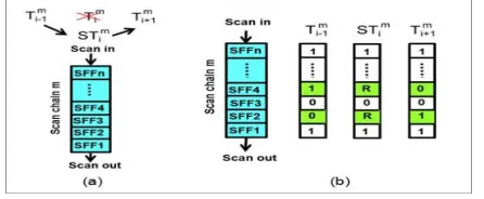
For each scan chain m ( m = 1 ... s ) , one Substitute Test Vector (STV) S𝑇𝑖𝑚 replaces the
original test vector 𝑇𝑖𝑚to be applied to the CUT at the I
th capture phase regarding to Conventional Logic BIST (Fig.3). In this method, the STV S𝑇𝑖𝑚to be asserted
in the Scan-Chain (SC) m and applied to the CUT at the ith capture phase is builded based on the structure of test vectors 𝑇𝑖−1𝑚 and 𝑇𝑖+1 𝑚 to be applied at
the ( i − 1)th and ( i + 1)th capture phases.
Fig. 3. (a) Sequence of STV filling each SC m, (b) bits in the STV S𝑇𝑖𝑚and in the Test Vectors applied
at the last/following capture phase (T m
i−1/T mi+1). Denoting by S𝑇𝑖𝑚 ( j ) , 𝑇𝑖−1𝑚 ( j ) ,and 𝑇𝑖+1𝑚 ( j) the logic
value of the j th bit in test vectors S𝑇𝑖𝑚 , 𝑇𝑖−1𝑚 ,and 𝑇𝑖+1𝑚 ,
respectively, STim ( j ) is chosen as follows 𝑆𝑇𝑖𝑚(𝑗) =
{𝑇𝑖−1
𝑚 (𝑗), 𝐼𝑓 𝑇
𝑖−1𝑚 (𝑗) = 𝑇𝑖+1𝑚
𝑅 , 𝐼𝑓 𝑇𝑖−1𝑚 (𝑗) ≠ 𝑇𝑖+1𝑚
where R denotes a random bit.
Therefore, in all bit positions j in which test vectors 𝑇𝑖−1𝑚 and 𝑇𝑖+1𝑚 , present the same logic value S𝑇𝑖𝑚
maintains the same logic value as in the prior test vector 𝑇𝑖−1𝑚 . First , in the bit positions j in which TV
𝑇𝑖−1𝑚 and 𝑇𝑖+1𝑚 differ, and S𝑇𝑖𝑚assumes a random
logic value R . The bit R can simply come from one of the outputs of the LFSR. Beginning from the (i − 1) th capture phase (Fig. 3), the STV sequence in each scan chain m will be as follows :
𝑇𝑖−1𝑚 − 𝑆𝑇𝑖𝑚− 𝑇𝑖+1𝑚 − 𝑆𝑇𝑖+2𝑚 − 𝑇𝑖+3𝑚 …….
Therefore, the number of bits changing logic value between the following test vectors with the new sequence 𝑇𝑖−1𝑚 − 𝑆𝑇𝑖𝑚− 𝑇𝑖+1𝑚 will be same, or lesser
than, those with the earliest TV sequence 𝑇𝑖−1𝑚 −
𝑇𝑖𝑚−𝑇𝑖+1𝑚 of Conventional LBIST.
The random bit R in 𝑆𝑇𝑖𝑚in the bit positions where
𝑇𝑖−1𝑚 and 𝑇
𝑖+1𝑚 differ allows the new sequence
Available online: https://edupediapublications.org/journals/index.php/IJR/ P a g e | 2296
original sequence. Therefore, the number of test
vectors required to achieve a target FC does not increase compared with the application of the original test sequence. The maximum CF between the following test vectors loaded in each SC in Conventional LBIST (𝐶𝐹𝑐𝑜𝑛𝑆𝐶 ) is reduced to a
half(𝐶𝐹𝑐𝑜𝑛𝑆𝐶/2) by this approach. Consequently,
denoting by 𝐶𝐹 𝑆𝑇𝑡𝑜𝑡 the maximum CF between any two
successive test vectors applied to the CUT at successive capture phases, for our approach with ST vector, it is as follows,
𝐶𝐹 𝑆𝑇𝑡𝑜𝑡=𝐶𝐹𝑐𝑜𝑛𝑡𝑜𝑡/2
Where 𝐶𝐹𝑆𝑇𝑡𝑜𝑡is the max CF obtained.
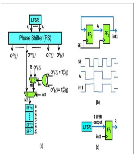
The presence of a Phase Shifter feeding the scan-chains of the CUT. Denoting by 𝑂𝑚 (m = 1 ...s) the Phase
Shifter output feeding the scan chain m, the logic value 𝑇𝑖𝑚(j) in the jth position of the ith test vector of the
scan chain m is given by
𝑇𝑖𝑚(𝑗) = 𝑂𝑚(𝜉) (1)
where ξ = n(i − 1) + j is the overall number of shift CKs from the starting of the test. By this way, the values loaded in the jth position of SC m in the shift phases before the (i-1) th, the ith, and the (i + 1)th capture phases will be well matched to the logic value present at the output 𝑂𝑚of the Phase Shifter, after ξ −
n, ξ, and ξ + n shift CKs, respectively, counted from the beginning of the test. Thus, for each SC m and capture phase i, we can express the logic values present in the jth position of the previous and the next test vectors 𝑇𝑖−1𝑚 (j) and 𝑇𝑖+1𝑚 (j), respectively as
𝑇𝑖−1𝑚 (𝑗) = 𝑂𝑚(𝜉 − 𝑛); 𝑇𝑖+1𝑚 (𝑗) = 𝑂𝑚(𝜉 + 𝑛). (2)
Since the Phase Shifter gives to its outputs many past/future values of each output 𝑂𝑚, we can determine
the values of 𝑂𝑚(ξ − n) and 𝑂𝑚(ξ + n) from the current
value present at two proper Phase Shifter outputs. Therefore, there exist two PS outputs 𝑂𝑘and 𝑂𝑝, with k
= p = m, such that
𝑂𝑚(𝜉 − 𝑛) =
𝑂𝑘(𝜉); 𝑂𝑚(𝜉 + 𝑛) = 𝑂𝑃(𝜉). (3)
The equations in (2) and (3) are used in deriving a existing method.
As an example, Fig. 4(a) shows a possible implementation of existing method, for the case in which the depth of the longest chain(s) is n.
Fig. 4. (a) Schematic of existing method (b) possible scheme to generate signal int1, and (c) strategy to generate the random bit R.
This method consists two multiplexers (M1 and M2) and an XOR gate for each scan chain m. M2 allows us to load the following in the scan chain m:
1) Either the test vectors 𝑇𝑖−1𝑚 and 𝑇𝑖+1𝑚 generated by
the Phase Shifter during the shift phases before the (i −1)th and (i +1)th capture phases, by setting the selection signal int1 = 0;
2) Or the Substitute Test vector 𝑆𝑇𝑖𝑚provided by
M1 during the shift phases before the ith capture phase, by setting int1 = 1. Particularly, the signal int1 is generated in such a way that it switches from 0 to 1 (and vice versa) at the following capture phases. The XOR gate used to compare the logic value at the PS output 𝑂𝑘(ξ ) [equal to 𝑇
𝑖−1𝑚 (j)] with the logic value
at the PS output 𝑂𝑝(ξ ) [equal to 𝑇
𝑖+1𝑚 (j)] at each shift
Available online: https://edupediapublications.org/journals/index.php/IJR/ P a g e | 2297
In Fig. 4(b) int1 generation is depicted, where FF1
and FF2 denote D FFs. At first, set FF1 to 1 and FF2 to 0 (int1 = 0). FF1 and FF2 are clocked by the SE signal. Thus, at each Scan Enable rising edge, int1 switches from 0 to 1 at intervals.
And in Fig. 4(c) a realizable scheme is shown to generate the bit R. One LFSR output feeds an FF (FF3), which is clocked by the int1 signal. At each rising edge of int1, FF3 samples on R a new value present at the considered LFSR output, and it keeps it till the following int1 rising edge. This way, the similar
R value is used during a entire shift phase.
This scheme used to generate R results in a highly unequal number of 0s or 1s in each Substitute Test vector, depending on whether R is 0 or 1.
IV. PROPOSED SYSTEM
In the extension method to reduce the area of the LOGIC BIST LP-LFSR is used in the place of normal LFSR based architecture which resulted in high fault coverage and the area of the scan based Logic BIST is diminished.
Fig.5.BLOCK DIAGRAM of PROPOSED SYSTEM A block diagram of proposed system consists of SEVEN Blocks. They are:
1. BIST CONTROLLER (BC)
A BC is used to generate the test vectors to activate all the blocks. It plays crucial role in LBIST. Whenever an IC is powered up (signal start BIST is made active) the controller starts the BIST procedure. Once the test is over, the status line is made high if fault is found.
2. PSEUDO RANDOM PATTERN GENERATOR(PRPG):
Vector from BC is used to initialize the PRPG block. In this paper, PRPG is implemented by using LP-LFSR. PRPG generates the test patterns in random manner which are fed to the circuit to be tested.
LP-LFSR:
In this paper we designed a novel architecture with Low Power Linear feedback shift register [LP-LFSR] which generates test patterns with reduced circuit activities reduces the power and uses only one flip-flop during shift operation to reduce the switching activities reduces the area.
In LP-LFSR, the counter is initialized with 0’s and generates test patterns in random sequence. A code generator and counter are controlled by common clock signal [CLK]. The output of counter is applied as input to a NOR-gate structure and a code generator. When all the bits of counter output are Zero, the NOR-gate output is one. Only when the NOR-gate output is one, the clock signal is applied to activate the LP-LFSR which generates the next sequence. The sequence generated from LP-LFSR is Exclusive–OR (XOR) with the sequence generated from code generator. The patterns generated from the Exclusive–OR (XOR) are the final output test patterns.
3. PHASE SHIFTER (PS):
The Phase Shifter (PS) is used to reduce the connection among the test vectors applied to adjacent scan-chains, is composed by an XOR network expanding the number of outputs of the LP- LFSR in order to match the number of scan chains
4. CIRCUIT UNDER TEST (CUT):
It is the major block where testing typically consists of applying set of test stimuli (input patterns and test vectors) and it consists of scan chains and combinational logic.
5. SPACE COMPACTOR (SC):
The Space Compactor compacts the outputs of the CUT to match the number of inputs of the MISR.
Available online: https://edupediapublications.org/journals/index.php/IJR/ P a g e | 2298
MISR produces compressed output that is
compared with the expected outputs (Golden signature) using a comparator to check for faulty or fault-free circuit.
7. TRUE RESPONSE ANALYZER (TRA) : TRA is the output of the circuit which compares or analyzes the test responses to determine correctness of the CUT. If TRA matches output is zero(pass) else 0 (fail).
By this way all the patterns get checked and if output is equal then we can say that CUT is working properly.
If the CUT is not faulty then test pin becomes zero that means testing is done and we can apply input to the CUT and we can use it.
V.
RESULTSCompared to using normal LFSR, by using LP-LFSR in proposed system the area is reduced compared to the existing system as shown in table 1, the number of flip-flops are reduced so area decreased by 72.5%
AREA ESTIMATED GRAPH
Fig.11. Overall Comparison of AREA between Existing and Proposed work
Different blocks of proposed system are designed coded in VERILOG HDL, simulated in I simulator and Xilinx ISE is the software tool used for FPGA synthesis..
RTL SCHEMATIC
TECHNOLOGY SCHEMATIC
Available online: https://edupediapublications.org/journals/index.php/IJR/ P a g e | 2299
VI. CONCLUSION
This paper presents a novel SCAN BASED LBIST architecture where every component is implemented and simulated using Xilinx 13.2. Software and ISimulator. The Scan Based LBIST circuit is designed using Low Power LFSR. Here LP- LFSR is used as a pseudorandom sequence generator, TRA is used to make verification of the circuit and Signature Analysis gives High Fault Coverage. Proposed architecture gives better performance than the existing method by 72.5% area is diminshed.
REFERENCES
[1] J. Rajski, J. Tyszer, G. Mrugalski, and B. Nadeau-Dostie, “Test generator with preselected toggling for low power built-in self-test,” in Proc. Eur. Test Symp., May 2012, pp. 1–6.
[2] Y. Sato, S. Wang, T. Kato, K. Miyase, and S. Kajihara, “Low power BIST for scan-shift and capture power,” in Proc. IEEE 21st Asian Test Symp., Nov. 2012, pp. 173–178.
[3] E. K. Moghaddam, J. Rajski, M. Kassab, and S. M. Reddy, “At-speed scan test with low switching activity,” in Proc. IEEE VLSI Test Symp., Apr. 2010, pp. 177–182.
[4] S. Balatsouka, V. Tenentes, X. Kavousianos, and K. Chakrabarty, “Defect aware X-filling for low-power scan testing,” in Proc. Design, Autom. Test Eur. Conf. Exhibit., Mar. 2010, pp. 873–878. [5] I. Polian, A. Czutro, S. Kundu, and B. Becker, “Power droop testing,” IEEE Design Test Comput., vol. 24, no. 3, pp. 276–284, May/Jun. 2007.
[6] X. Wen et al., “On pinpoint capture power management in at-speed scan test generation,” in Proc. IEEE Int. Test Conf., Nov. 2012, pp. 1–10. [7] S. Kiamehr, F. Firouzi, and M. B. Tahoori, “A layout-aware X-filling approach for dynamic power supply noise reduction in at-speed scan testing,” in Proc. IEEE Eur. Test Symp., May 2013, pp. 1–6.
[8] M. Nourani, M. Tehranipoor, and N. Ahmed, “Low-transition test pattern generation for BIST-based applications,” IEEE Trans. Comput., vol. 57, no. 3, pp. 303–315, Mar. 2008.
[9] N. Z. Basturkmen, S. M. Reddy, and I. Pomeranz, “A low power pseudorandom BIST technique,” in Proc. 8th IEEE Int. On-Line Test. Workshop, Jul. 2002, pp. 140–144.
[10] J. Rajski, N. Tamarapalli, and J. Tyszer, “Automated synthesis of large phase shifters for built-in self-test,” in Proc. Int. Test Conf., Oct. 1998, pp. 1047–1056.
[11] P. Girard, L. Guiller, C. Landrault, S. Pravossoudovitch, and H. J. Wunderlich, “A modified clock scheme for a low power BIST test pattern generator,” in Proc. IEEE VLSI Test Symp., Apr./May 2001, pp. 306–311.
[12] G. Hetherington, T. Fryars, N. Tamarapalli, M. Kassab, A. Hassan, and J. Rajski, “Logic BIST for large industrial designs: Real issues and case studies,” in Proc. Int. Test Conf., 1999, pp. 358–367. [13] M. Tehranipoor, M. Nourani, and N. Ahmed, “Low transition LFSR for BIST-based applications,” in Proc. 14th Asian Test Symp., Dec. 2005, pp. 138–143.
[14] Y. Huang and X. Lin, “Programmable logic BIST for at-speed test,” in Proc. 16th Asian Test Symp., Oct. 2007, pp. 295–300. [15] X. Lin, E. Moghaddam, N. Mukherjee, B. Nadeau-Dostie, J. Rajski, and J. Tyszer, “Power aware embedded test,” in Proc. IEEE Asian Test Symp., Nov. 2011, pp. 511–516.
[16] X. Lin, “Power supply droop and its impacts on structural at-speed testing,” in Proc. 21st Asian Test Symp., Nov. 2012, pp. 239– 244.
[17] Mentor Graphics. (2011). Tessent LogicBIST: At-Speed Pseudorandom Pattern Embedded Logic Test. [Online]. Available: http://www.mentor. com/products/silicon yield/pro ducts/ upload/logicbist-ds.pdf
[18] B. Nadeau-Dostie, K. Takeshita, and J.-F. Cote, “Power-aware at-speed scan test methodology for circuits with synchronous clocks,” in Proc. IEEE Int. Test Conf., Oct. 2008, pp. 1–10, paper 9.3. [
19] M. Omaña, D. Rossi, E. Beniamino, C. Metra, C. Tirumurti, and R. Galivanche, “Power droop reduction during launch-on-shift scanbased logic BIST,” in Proc. IEEE Int. Symp. Defect Fault Tolerance VLSI Nanotechnol. Syst., Oct. 2014, pp. 21–26. [20] M. Omaña, D. Rossi, E. Beniamino, C. Metra, C. Tirumurti, and R. Galivanche, “Low-cost and high-reduction approaches for power droop during launch-on-shift scan-based logic BIST,” IEEE Trans. Comput., to be published.
[21] J. Rajski, J. Tyszer, G. Mrugalski, and B. Nadeau-Dostie, “Test generator with preselected toggling for low power built-in self-test,” in Proc. IEEE VLSI Test Symp., Apr. 2012, pp. 1–6.
[22] E. Kalligeros, D. Kaseridis, X. Kavousianos, and D. Nikolos, “Reseeding-based test set embedding with reduced test sequences,” in Proc. IEEE Int. Symp. Quality Electron. Design, Mar. 2005, pp. 226–231.
[23] M. Omaña, D. Rossi, F. Fuzzi, C. Metra, C. Tirumurti, and R. Galivache, “Novel approach to reduce power droop during scan-based logic BIST,” in Proc. IEEE Eur. Test Symp. (ETS), May 2013, pp. 1–6.
[24] M. Zhang et al., “Sequential element design with built-in soft error resilience,” IEEE Trans. Very Large Scale Integr. (VLSI) Syst., vol. 14, no. 12, pp. 1368–1378, Dec. 2006.
Available online: https://edupediapublications.org/journals/index.php/IJR/ P a g e | 2300
[26] X. Lin, R. Press, J. Rajski, P. Reuter, T. Rinderknecht,
B.Swanson, and N. Tamarapalli, "High-Frequency, At-Speed Scan Testing," in D&T of Computers, Sept.- Oct. 2003, pp. 17-25.
[27].Gerstendörfer S. and Wunderlich H. -J., ‘Minimized power consumption for scan-based BIST,’ J. Electron. Test., vol. 16, no. 3, pp. 203, July1999.
[28] B. Koenemann, “LFSR-Coded Test Patterns for Scan Design,” in Proc. European Test Conf., 1991, pp. 237-242. [29] V.Harish, S.Sowjanya. “Power Optimization of LFSR for fault coverage circuit with efficient hardware utilization”, IJCSIET--International
Journal of Computer Science information and Engg., Technologies ISSN 2277-4408 || 01112014-038. [30] Nagaraj s vannal, saroja v siddamal, shruti v bidaralli, mahalaxmi sbhille, “Design and testing of combinational Logic circuits using built in self Test scheme for fpgas,” 2015 fifth international conference on communication systems and network technologies, 2015.
[31]Swapna S, Sunilkumar S Manvi, “Review of LP-TPG
Using LP-LFSR for Switching Activities”, Volume 5, Issue 2, February 2015 ISSN: 2277 128X ,International Journal of Advanced Research in Computer Science and Software Engineering.