Design and Implementation of Low Power Single Phase Clock
Distributon
B.Vidya Sagar Goud & Mr. G.Sai Kumar
1.Pg Scholar, Department Of Ece, Ashoka Institute Of Engineering And Technology Malkapur(V), Choutuppal(M), Nalgonda(D)
2.Assistant Professor, Department Of Ece, Ashoka Institute Of Engineering And Technology Malkapur(V), Choutuppal(M), Nalgonda(D)
ABSTRACT
The clock distribution network consumes nearly 70% of the total power consumed by the IC since this is the only signal which has the highest switching activity. Normally for a multi clock domain network we develop a multiple PLL to cater the need, this project aim for developing a low power single clock multiband network which will supply for the multi clock domain network. This project is highly useful and recommended for communication applications like Bluetooth, Zigbee. WLAN frequency synthesizers are proposed based on pulse-swallow topology and the designed is modeled using Verilog simulated using Modelsim and implemented in Xilinx.
I INTRODUCTION
LAN (WLAN) in the multigigahertz bands such as HiperLAN II and IEEE 802.11a/b/g, are recognized as leading standards for high-rate data transmissions, and standards like IEEE802.15.4 are recognized for low-rate data
power compared to static dividers. The TSPC and E-TSPC designs are able to drive the dynamic latch with a single clock phase and avoid the skew problem. However, the adoption of single-phase clock latches in frequency dividers has been limited to PLLs with applications below 5 GHz ..Proposed dynamic logic multiband flexible Divider. The frequency synthesizer uses an E-TSPC prescaler as the first-stage divider, but the divider consumes around 6.25 mW. Most IEEE 802.11a/b/g frequency synthesizers employ SCL dividers as their first stage while dynamic latches are not yet adopted for multiband synthesizers. In this paper, a Dynamic logic multiband flexible integer-n divider based on pulse-swallow topology is proposed which uses a low-power wideband 2/3 prescaler and a wideband multimodulus 32/33/47/48 prescaler as shown in Fig.1 The divider also uses an improved low power loadable bit-cell for the Swallow S-counter. II.DESIGN CONSIDERATIONS
The key parameters of high-speed digital circuits are the propagation delay and power consumption. The maximum operating frequency of a digital circuit is calculated and is given by
f max = 1/tpLH+tpHL (1)
Where tpLH and tpHL are the propagation delays of gates, respectively. The total power consumption of the CMOS digital circuits is determined by the switching and short circuit power. The switching power is linearly Wproportional to the operating frequency and is given by the sum of switching power at each output node as in P
switching = ∑ fclkCLiV 2 dd (2)
Where n is the number of switching nodes, fclk is the clock frequency,CLi the load capacitance at the output node of the ith stage, and vdd is the supply voltage. Normally the shortcircuit power occurs in dynamic circuits when there exists direct paths from the supply to ground which is given by
PSC=ISC*vdd (3)
capacitance, but it consumes significantly more power than the TSPC circuit does for a given transistor size. The following analysis is based on the latest design using the popular and low-cost 0.18µ CMOS process.
A.Swallow (S) Counter The 6-bit s-counter shown in Fig.4.consists of six asynchronous loadable bit-cells, a NOR-embedded DFF and additional logic gates to allow it to be programmable from 0 to 31 for low-frequency band and from 0 to 47 for the highfrequency band. The asynchronous bit cell used in this design shown in Fig.4.is similar to the bit-cell except it uses two additional transistors M6 and M7whose inputs are controlled by the logic signal MOD. If MOD is logically high, nodes S1 and S2 switch to logic “0” and the bit-cell does not perform any function. The MOD signal goes logically high only when the S-counter finishes counting down to zero. If MOD and LD are logically low, the bit-cell acts as a divide-by-2 unit. If MOD is logically low and LD is logically high, the input bit PI is transferred to the output. In the initial state, MOD=0, the multimodulus prescaler selects the divide-by-N+1 mode (divide-by-33 or divide-by- 48) and P, S counters start down counting the input clock cycles. When the S-counter finishes counting, MOD switches to logic “1” and the prescaler changes to the divide-by-n mode (divide-by-32
or divide-47) for the remaining P-S clock cycles. During this mode, since Scounter is idle, transistors M6 and M7 which are controlled by MOD, keep the nodes S1 and S2 at logic “0,” thus saving the switching power in S-counter for a period of (N*(P-S)) clock cycles. Here, the programmable input (PI) is used to load the counter to a specified value from 0 to 31 for the lower band and 0 to 48 for the higher band of operation.
III. Programmable (P) Counter
(2.4 GHz) while an 8-bit S-counter would be needed for the high frequency band(5–5.825 GHz) with a fixed 5-bit S-counter. Thus, the multimodulus32/33/47/48 prescaler eases the design complexity of the P-counter.
1)When Sel=‟0‟: When Sel=‟0‟ the output from N4 gate is given to the prescaler and the multimodulus prescaler selects 32/33 mode and the division ratio is controlled by MOD signal. When MOD=1 the output from N4 gate switches to logic „1‟ and the prescaler operates in divide-by-2 for entire operation. i.e., now division ratio of 32 (N) is performed. Similarly when MOD=0, MC remains high for first 30 input clock cycles and goes low for 3 input clock cycles. Thus division ratio of 33(N+1) is performed. N and
N+1 are given by 32 (AD*N1) N 331))
(1*(N11)*N1) ((AD 1N 2)When Sel=1: When Sel=1, the inverted output from N4 gate is given to the input of 2/3 prescaler and multimodulus prescaler operates in 47/48 mode. MOD signal controls the division ratio. When MOD=1 and MC=1 prescaler operated in divide-by-3 for the entire input cycles and division ratio of 48(N+1) is performed. When MOD=1 and MC=0 divideby- 2 is selected for entire input clock cycles for prescaler and the division ratio of 47(N) is performed. N and N+1 are given by 1
IV.SIMULATION RESULTS
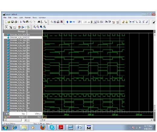
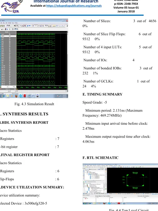
Fig. 4.1 Simulation Result
Fig. 4.3 Simulation Result
A. SYNTHESIS RESULTS
B.HDL SYNTHESIS REPORT
Macro Statistics
# Registers : 7
1-bit register : 7
C.FINAL REGISTER REPORT
Macro Statistics
# Registers : 6
Flip-Flops : 6
D.DEVICE UTILIZATION SUMMARY:
Device utilization summary:
Selected Device : 3s500efg320-5
Number of Slices: 3 out of 4656 0%
Number of Slice Flip Flops: 6 out of 9312 0%
Number of 4 input LUTs: 5 out of 9312 0%
Number of IOs: 4
Number of bonded IOBs: 3 out of 232 1%
Number of GCLKs: 1 out of 24 4%
E. TIMING SUMMARY
Speed Grade: -5
Minimum period: 2.131ns (Maximum Frequency: 469.274MHz)
Minimum input arrival time before clock: 2.470ns
Maximum output required time after clock: 4.063ns
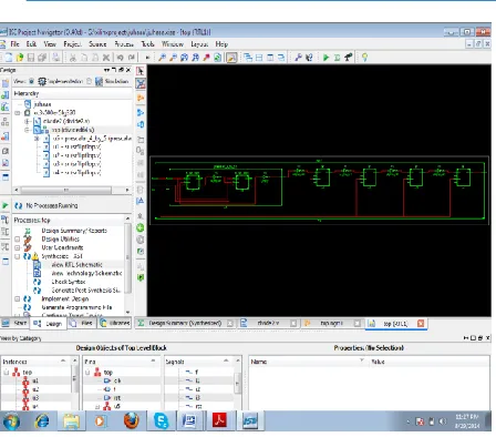
F. RTL SCHEMATIC
Fig4.5 Rtl Schematic diagram
G.TECHNOLOGY SCHEMATIC
Fig. 4.6 Technology Schematic
IV CONCLUSION
In this paper, a wideband 2/3 prescaler is verified in the design of proposed wide band multi modulus 32/33/47/48 prescaler. A dynamic
logic multiband flex-ible integer N divider is designed which uses the wide-band 2/3 prescaler, multi modulus 32/33/47/48 prescaler, and is silicon verified using the 0.18μm CMOS technology. Since the multi modulus 32/33/47/48 prescaler has maximum operating frequency of 6.2 GHz, the values of P- and S-counters can actually be programmed to divide over the whole range of frequencies from 1 to 6.2 GHz with finest resolution of 1 MHz and variable chan-nel spacing. However, since interest lies in the 2.4- and 5–5.825-GHz bands of operation, the P- and S-counters are programmed accordingly. The proposed multiband flexible divider also uses an improved loadable bit-cell for Swallow S-counter and consumes a power of 0.96 and 2.2 mW in 2.4- and 5-GHz bands, respectively, and provides a solution to the low power PLL synthesizers for Bluetooth, Zigbee, IEEE 802.15.4, and IEEE 802.11a/ b/g WLAN applications with variable channel spacing.
REFERENCES:
1.H. R. Rateghet al., “A CMOS frequency synthesizer with an injectedlocked frequency divider for 5-GHz wir-less LAN receiver,” IEEE J. Solid-State Circuits, vol. 35, no. 5, pp. 780– 787, May 2000.
divider and differential switched capacitors,” IEEE Trans. Circuits Syst. I, Reg. Papers, vol. 56, no. 2, pp. 320–326, Feb. 2009.
3.L. Lai Kan Leung et al., “A 1-V 9.7-mW CMOS fre-quency synthesizer for IEEE 802.11a transceivers,” IEEE Trans. Microw. Theory Tech., vol. 56, no. 1, pp. 39–48, Jan. 2008. 4.M. Alioto and G. Palumbo, Model and Design of Bipo-lar and MOS Current-Mode Logic Digital Circuits. New York: Springer, 2005. 5.Y. Ji-renet al., “Atrue single-phase-clock dynamicC-MOScircuit technique,” IEEE J. Solid-State Circuits, vol. 24, no. 2, pp. 62–70, Feb.1989.
6.S. Pelleranoet al., “A 13.5-mW 5 GHz frequency synthesizer with dynamic-logic frequency divider,” IEEE J. Solid-State Circuits, vol. 39, no. 2, pp. 378– 383, Feb. 2004.
7.V. K. Manthenaet al., “A low power fully program-mable 1 MHz resolution 2.4 GHz CMOS PLL frequency synthesizer,” in Proc. IEEE Biomed. Circuits Syst. Conf., Nov. 2007, pp. 187–190.
8.S. Shin et al., “4.2 mW frequency synthesizer for 2.4 GHz ZigBee application with fast settling time performance,” in IEEE MTT-S Int. Microw. Symp. Dig. , Jun. 2006, pp. 411–414.
9.S. Vikaset al., “1 V 7-mW dual-band fast-locked frequency synthesizer,” in Proc. 15th ACM Symp. VLSI, 2005, pp. 431–435.
10. V. K. Manthenaet al., “A 1.8-V 6.5-GHz low power wide band singlephase clock CMOS 2/3 prescaler,” in IEEE 53rd Midwest Symp. Circuits Syst., Aug. 2010, pp. 149–152.
11.J. M. Rabaeyet al., “Digital integrated circuits, a design perspective,” in Ser. Electron and VLSI, 2nd ed. Upper Saddle River, NJ: Prentice- Hall, 2003. 12.X. P. Yu et al., “Design and optimization of the extended true singlephase clock-based prescaler,” IEEE Trans. Microw. Theory Tech., vol. 56, no. 11, pp. 3828–3835, Nov. 2006.