Do-254 Implementation of High Speed Vedic
Multiplier
Shashidhar Shivanagi1, Dr. A.B.Kalpana2, Kumaraswamy KV3
PG Student [VLSI], Dept. of ECE, Bangalore Institute of Technology, Bangalore, Karnataka, India1
Assistant Professor, Dept. of ECE, Bangalore Institute of Technology, Bangalore, Karnataka, India2
Technical Manager, Trident Tech Labs, Bangalore, Karnataka, India3
ABSTRACT: We know that the multipliers have an important role in applications like filters, ALUs, that the multiplier should be very high speed. This paper presents the high speed Vedic Multiplier which has modified architecture with carry save adders (CSAs). The proposed Vedic Multiplier gives better results as compared to conventional multipliers. The design is implemented in Verilog according to DO-254 coding guidelines, simulated with industrial standard simulator QuestaSim and synthesized using a combination of Precision Synthesis RTL Plus and Xilinx ISE. DO-254 standard compliance is done using Mentor’s HDL Designer tool suite. The adder sub block gives a speed of 3.597ns which is 57.88%, 76.39%, 82% improvement than the existing adder for 8-bit, 16-bit and 32-bit adder respectively. Area of the adder has been reduced by 8.96% for 8-bit, 45.28% for 16-bit and 22.42% for 32 bit. The performance of proposed multiplier block has risen by 85%, 89.67% and 94.17% for 8-bit, 16-bit and 32-bit respectively. This improvement in performance trades off with a slight increase in area of 17%, 12% and 14% for 8-bit, 16-bit and 32-bit multiplier block respectively, DO-254 compliance done.
KEYWORDS: FIR filter, Vedic multiplier, Carry Save Adder, DO-254
I.INTRODUCTION
Any kind of processors needs the high speed multipliers. It is observed that the computers, mobiles stop working suddenly. The main reason behind this is the processors which are in the computers and mobiles are slow. To increase the speed of the processors it needs the high speed multipliers. This reason gave more interest to design high speed multipliers. In many of the applications like multiply and accumulate (MAC), Processors, Filters the multipliers role is very important.
In[1] few decades the multipliers have been designed but these multipliers have more cross product terms and the they have more area, power and also more time to give the expected output results. The more delay reason behind this is that the critical path increase because of more incomplete products.
In [2][3][4] and [5] a new approach multiplier design based on the Vedic mathematics sutras to overcome these fash. Vedic mathematics is a primitive and well-known approach that gives laudable solutions. Swami Barathi Krishna Tirthaji Maharaj(1884-1960) is a putative mathematician found and isolated primitive Vedic mathematics into 16 simple sutras(formulae) those are related to Analytical, Geometry, algebra, arithmetic. These sutras can be applicable in different fields of engineering.
In Vedic mathematics the incomplete products are calculated quickly and added by using the adders accordingly. The paper introduces the high speed Vedic multiplier using the Uradhva Tiryakbhyam sutra. It uses the Carry Save Adders (CSAs) to add the incomplete product which exaggerates the speed of the multiplier.
II.RELATED WORK
A. VEDIC MATHEMATICS
There are four Vedas, i) Rigveda, ii)Yajurvaeda, iii) Samaveda, iv) Atharvaveda. Merlot which is Atharvaveda is an origin of 16 formulae of Vedic mathematics.
Vedic mathematics is very interesting topic. The Vedic mathematics consumes less time to calculate any problems, because of this it has become more and more putative and it is very simple one. In this Atharvaveda there are 16 sutras one of which is Uradhva Tiryakbhyam. This sutra generates the incomplete products concurrently. The Uradhva Tiryakbhyam is the Sanskrit word which stands for vertically and crosswise. The Fig.1 clearly interprets the method of multiplication using the Uradhva Tiryakbhyam for two 8 bit numbers dot multiplication.
B. CARRY SAVE ADDER
There are many different kind of adders are present to add the numbers. To add ‘m’ numbers of ‘n’ bit wide, first it adds two numbers then adds this result with the next number and so on till the ‘m’ number. This kind of addition consumes m-1 adders for the gate delay of O(mlgn). Instead add the numbers with the help of tree structures the gate delay is of O (lgm.lgn).
With the help of Carry Save Adder the delay still more reduces. This Carry Save Adder takes three numbers at a time to add instead of two numbers. Suppose the three numbers x+y+z then carry save adder will convert it into two numbers c+s such that x+y+z=c+s, and the total gate delay will be of O(1) time. In carry save adder, instead of propagating the carries to the next step that saves it till the very last step.
Fig1. Depicts of two 8 bit numbers multiplication using Uradhva Tiryakbhyam sutra.
The Fig.2 depicts the addition of three 8 bit numbers using the Carry Save Adder. The vital point in CSA is that, the each c and s can be found independently from all other carries and sum bits. This is called (3,2) counter because it makes three numbers into two.
We need m-2 CSA blocks to add m numbers and each CSAs blocks may have many one bit CSA in parallel. Finally we need Carry Lookahead Adder (CLA) as the carry propagation block. Note that each time we enter into CSA block the number increases in size by 1 bit. Because of this reason till the CLA block the number will be at most n+m-2 bits. The last CLA will take the gate delay of O(lg(n+m))time. Therefore the final sum will be with gate delay of O(m+lg(n+m)).
C. INTRODUCTION TO DO-254
DO-254 is a standard guidance for designing the avionics hardware. DO-254 is also called as DO254 or D0254. There are five design assurance levels(DAL) are present viz. level A, level B, level C, level D and level E.
To meet level A criteria, approximately design should meet 20 to 30% of systems and 40% of hardware implementation DO-254 compliance. To meet level B design should meet 20% of system, 30% of hardware implementation, for level C design should meet 25% of system, 20% of hardware implementation, for level D design should meet 20% of system, 10% of hardware implementation and for level Edesign should meet 10% of system, 5% of hardware implementation.
III. PROPOSED METHODOLOGY
The proposed multiplier is based on the Uradhva Tiryakbhyam sutra to get the incomplete products and these incomplete products will be added with help of the Carry Save Adders. In the first stage of addition of incomplete adders we have 8 bit CSA which are from {q0[7:4,4’b0},q1,q3. In the second stage of addition we have 9 bit CSA because {c1,1’b0},{1’b0,s1} and {1’b0,q3} will be added.
Then the last stage of addition CSA has the Carry Lookahaed Adder which is of 10 bit adder. The inputs for the last stage CLA are {c2,1’b0} and {1’b0,s2}.This gives lower nibble of the product directly from the q0 which is q0[3:0] and other 11 bits of product will be from the 10 bit Carry Lookahead Adder is as shown in Fig.3.
IV. RESULTS
To compare different adders performance, area of Ling adder, Brent Adder and Ripple Carry adder and the different multipliers like Vedic, Array and Booth multipliers[5] and the proposed Adder and the Multiplier were designed using the Verilog. Table-I is comparison of adders and Table II is comparison of multipliers
Simulation results of the three 8-bit carry save adder is as shown in Fig.4. The proposed Vedic multiplier is as shown in Fig.5
Three 8-bit numbers addition Technical Schematic of Carry Save Adder is as shown in Fig.6. Three 8-bit Number additions RTL Schematic of Carry Save Adder is as shown in Fig.7
Fig4. Three 8-bit numbers addition simulation result of Carry Save AdderFig 5. 8x8 proposed Vedic Multiplier Simulation result Save Adder
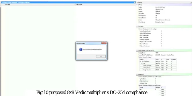
The 8x8 proposed Vedic Multiplier Technical Schematic is as shown in Fig.8, 8x8 proposed Vedic Multiplier RTL Schematic is as shown in Fig.9 and 8x8 proposed Vedic multiplier’s DO-254 compliance is as shown in Fig.10
V.CONCLUSIONANDFUTUREWORK
In the proposed paper a modified Vedic multiplier has been implemented and is compared with the existing Vedic multiplier, Array multiplier and Booth multiplier. The modified Vedic multiplier architecture includes Carry save adders (CSAs). The adder sub block gives a speed of 3.597ns which is 57.88%, 76.39%, 82% improvement than the existing adder for 8-bit, 16-bit and 32-bit adder respectively. Area of the adder has been reduced by 8.96% for 8-bit, 45.28% for 16-bit and 22.42% for 32 bit. The performance of proposed multiplier block has risen by 85%, 89.67% and 94.17% for 8-bit, 16-bit and 32-bit respectively. This improvement in performance trades off with a slight increase in
Fig 8.Proposed 8x8 Vedic Multiplier TechnicalFig 9. Proposed 8x8 Vedic Multiplier RTL Schematic
Fig.10 proposed 8x8 Vedic multiplier’s DO-254 compliance
area of 17%, 12% and 14% for 8-bit, 16-bit and 32-bit multiplier block respectively, DO-254 compliance done. Further the multipliers can be extended to 64 bit, 128 bit.
REFERENCES
[1] Swee, K. L. S. , Lo HaiHiung, ”Performance Comparison Review of 32-Bit Multiplier Designs”, 4th International Conference on Intelligent and Advanced Systems (ICIAS), 2012 , IEEE proc. , vol. 2, pp 836-841
[2] Vengadapathiraj.MRajendhiran.V, Gururaj.M, VinothKannan.A, Mohamed Nizar.S. “DESIGN AND FPGA IMPLEMENTATION OF HIGH SPEED 128X 128 BITS VEDIC MULTIPLIER USING CARRY LOOK-AHEAD ADDER”. International Journal of Advanced Research in Electronics and Communication Engineering (IJARECE) Volume 4, Issue 2, February 2015.
[3] Mr. Sumit C. Katkar, Prof. PragatiKene, Prof. ShubhanginiUgale,” DESIGN OF EFFICIENT 64 BIT MAC UNIT USING VEDIC MULTIPLIER FOR DSP APPLICATION – A REVIEW”. ISSN 2348 – 9928 IJAICT Volume 1, Issue 9, January 2015 Doi:01.0401/ijaict.2015.09.07 Published on 05 (02) 2015.
[4] C. Suba, S. Karthick, M. Prakash, “Analysis of Different Bit Carry Lookahead Adder with Reconfigurability in Low Power VLSI Using Verilog Code”. International Journal of Innovative Research in Computer and Communication Engineering (An ISO 3297: 2007 Certified Organization) Vol. 2, Issue 11, November 2014 Copyright to IJIRCCE www.ijircce.com 6365.
[5] DeepaYagain, Dr. Vijaya Krishna A, “FIR Filter Design Based on Retiming & Automation Using VLSI Design Metrices”. 2013 International Conference on Technology,Informatics,Management, Engineering & Environment (TIME-E 2013) Bandung, Indonesia,June 23-26,2013 [6] VaijyanathKunchigi, LinganagoudaKulkarni ,Subhash Kulkarni,”32-BIT MAC UNIT DESIGN USING VEDIC MULTIPLIER”. International
Journal of Scientific and Research Publications, Volume 3, Issue 2, February 2013 1 ISSN 2250-3153.
[7] P.Jagadeesh Mr.S.avi Dr. Kittur Harish Mallkarjun, “Design of High performance 64 bit MA Unit. 2013 Interntional Conference on Circuits, Power and Computing Technologies [ICCPCT-2013].
[8] G.Ganesh Kumar, V.Charishma,” Design of High Speed Vedic Multiplier using Vedic Mathematics Techniques”. International Journal of Scientific and Research Publications, Volume 2, Issue 3, March 2012 1 ISSN 2250-3153
[9] ArushiSomani, Dheeraj Jain, Sanjay Jaiswal, KumkumVerma and Swati Kasht,” Compare Vedic Multipliers with Conventional Hierarchical array of array multiplier”. International Journal of Computer Technology and Electronics Engineering (IJCTEE) Volume 2, Issue 6.
[10] SumitVaidya and Deepak Dandekar, “DELAY-POWER PERFORMANCE COMPARISON OF MULTIPLIERS IN VLSI CIRCUIT DESIGN. International Journal of Computer Networks & Communications (IJCNC), Vol.2, No.4, July 2010.
[11] Anveshkumar, Ashishraman, “Low Power ALU Design by Ancient Mathematics” 978-1-4244-5586-7/10/$26.00 2010 IEEE. [12] Prof. Loh, “Carry-Save Addition” CS3220 - Processor Design - Spring 2005 February 2, 2005.
[13] Rundal Fulton, Roy Vandermolen, “Airborne Electronic Hardware Design Assurence” CRC Press Taylor & Francis Group Boco Raton London New York.
BIOGRAPHY
Shashidhar Shivanagireceived his B.E. degree in Electronics and Communication Engineering from East Point College of Engineering and Technology in 2013. He is presently pursuing his final year M.Tech in VLSI Design and Embedded Systems from Bangalore Institute of Technology and the proposed research work in this paper is part of his M.Tech thesis. His area of interestsincludes very-large-scale integration digital circuit design and Verilog based projects.
Dr. A.B.Kalpana received B.E, Degree from Bangalore University, In 1995, M.E, Degree from U.V.C.E, Bangalore in 2001, Ph.D in 2014 in the Department of Applied Electronics, Gulbarga University, Gulbarga, INDIA.Currently she is working as Assistant Professor in the Department of Electronics and Communication, Bangalore Institute of Technology, Bangalore, INDIA, her research interests include Analysis and Design of VLSI circuits and power electronics. She has published up to18 national and international conference and journal papers.