A Variable Gain-CMOS Instrumentation
Amplifier: Case Study
Anuj Singh Yadav 1, D.K.Mishra2
M. Tech Student, E & I Department, Shri G.S. Institute of Technology and Science, Indore, India 1
Professor & Head, E & I Department, Shri G.S. Institute of Technology and Science, Indore, India2
ABSTRACT: In this paper we have designed and implement the variable gain instrumentational amplifier for high frequency application. Front end amplifier required to have a high input impedance through which intended current is measured, signal coming from the tissue of human body is applied to an IA through electrodes, before going for an imaging. So that the signal can be boost up, detectable and immune to noise. For imaging of cancer biomarkers it is necessary to measure bioimpedance over a wide range of frequency 10 KHz to 2 MHz. The circuit is intended for a wideband bioimpedance imaging application, required gain up to 40dB. Other than this it is giving a 100 dB CMRR at the high frequency of 8MHz with low power dissipation of 567 μw, low input referred noise and minimum area of
0.000985 mm-square. This local current feedback variable gain IA is compared with two IA (Current feedback IA and indirect current feedback IA) and is comparatively more stable, higher CMRR value. This amplifier is a boon to bioimpedance imaging, EIT and other bio-medical applications.
KEYWORDS: Cancer biomarkers, CMOS, bioimpedance, high CMRR, instrumentation amplifier (IA), local current feedback, imaging, Electrical Impedence Tomography (EIT), Electro Cardio Graph (ECG).
I. INTRODUCTION
Instrumentation amplifiers (in-amps) amplify the difference between two signals. These differential signals typically emanate from sensors such as resistive bridges or thermocouples.
An instrumentation (or instrumentational) amplifier is a type of differential amplifier that has been outfitted with input buffer amplifiers, which eliminate the need for input impedance matching and thus make the amplifier particularly suitable for use in measurement and test equipment. Additional characteristics include very low DC offset, low drift, low noise, very high open-loop gain, very high common-mode rejection ratio, and very high input impedances. Instrumentation amplifiers are used where great accuracy and stability of the circuit both short and long-term are required.
The specification of common mode rejection ratio (CMRR) is a measure of the extent to which common mode signals are rejected by an amplifier. An instrumentation amplifier is a closed-loop gain block that has a differential input and an output that is single-ended with respect to a reference terminal. Most commonly, the impedances of the two input terminals are balanced and have high values, typically 1000G ohms, or greater. The input bias currents should also be low, typically 1 nA to 50 nA. As with operational amplifiers, output impedance is very low, nominally only a few milliohms, at low frequencies. Unlike an op amp, for which closed-loop gain is determined by external resistors connected between its inverting input and its output, an in-amp employs an internal feedback resistor network that is isolated from its signal input terminals. With the input signal applied across the two differential inputs, gain is either preset internally or is user set (via pins) by an internal or external gain resistor, which is also isolated from the signal inputs.
impedence to avoid the part of produced current into the circuit, which would cause erroneous faults. Thus IA is required. The main focus is on to detect the micro volts (μvolts) differential signal of the body tissue in the presence of milli-volts (mv) common mode interring signal at working frequency of few Hz to MHz.
Common-mode rejection (CMR), the property of cancelling out any signals that are common (the same potential on both inputs), while amplifying any signals that are differential (a potential difference between the inputs), is the most important function of an instrumentation amplifier provides. Both dc and ac common-mode rejection are important in-amp specifications. Any errors due to dc common-mode voltage (i.e., dc voltage present at both inputs) will be reduced 80 dB to 120 dB by any modern in-amp of decent quality. In-amps are widely used in medical equipment such as EKG and EEG monitors, blood pressure monitors, and defibrillators.
II. RELATED WORK
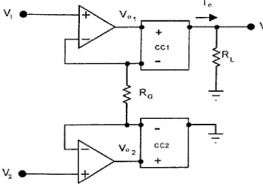
An enhanced current-mode instrumentation amplifier is shown in fig 1. The circuit is based on a current conveyor operational amplifier combined configuration that offers significant improvement in accuracy as compared with the basic current-mode instrumentation amplifier based on current conveyors only.
In Fig 1 It comprises of two op amps working in conjunction with current conveyors. In practice, this circuit will also need a buffered output. Each current conveyor has its input circuit within the negative feedback loop of an op amp. The high loop gain of the op amp ensures that the current through the input resistors Rx at the inverting inputs of the current conveyors is determined solely by the external resistor Rg in conjunction with the differential input voltage. The overall effect of this is Rx that is eliminated from the circuit transfer function.
Fig. 1: Current-mode instrumentation amplifier using operational amplifiers and current conveyors.
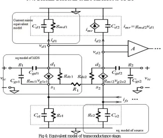
Fig. 2 shows the simplified circuit schematic of the local current feedback IA [17]. The input transconductor stage uses a simple current mirror load (drain network) and current source biasing (source network). The sensing amplifier serves to exactly balance the drain currents of transistors Mi1 and Mi2 by adjusting the complementary currents I1 and I2. A direct result of this is that the input differential voltage is forced across resistor R1 and hence Mi1 and Mi2 of the input stage essentially acts as a unity-gain buffer.
Fig. 2: Simplified model of a instrumentation amplifier with current feedback [17]
The common-mode gain characteristics of the IA due to random mismatches can be analyzed by focusing only on the input stage. This is because the mismatch effects of the sensing amplifier A and the output transcondutance stage are greatly suppressed by the high gain of the local feedback loops. Fig. 2 shows the small-signal model of the IA’s input stage where it is assumed that the output conductances of Md1, 2 are much less than their corresponding transconductances. The voltages at the drain terminals, d1 and d2, are sensed by the amplifier A which drives the differential feedback current ifs. The feedback path is via the source terminals s1 and s2. In the figure, gmi1,2 and gds1,2 are respectively the transconductances and drain-source conductances of the input transistors Mi1 and Mi2.gmd1,2 are the transconductances of the drain transistors Md1 and Md2.gs1,2 are the output conductances of the current sources I1 and I2 . All parasitic capacitances are included to allow a study of the high-frequency mismatch characteristics. Cs1,2 and Cd1,2 are respectively the gate-source and gate-drain capacitances of the input transistors Mi1 and Mi2, and Cs1,2 and Cd1,2 are respectively the total capacitances of the source and drain terminals, including those from the input and load/source transistors as well as the amplifier stages that are connected to the terminals.
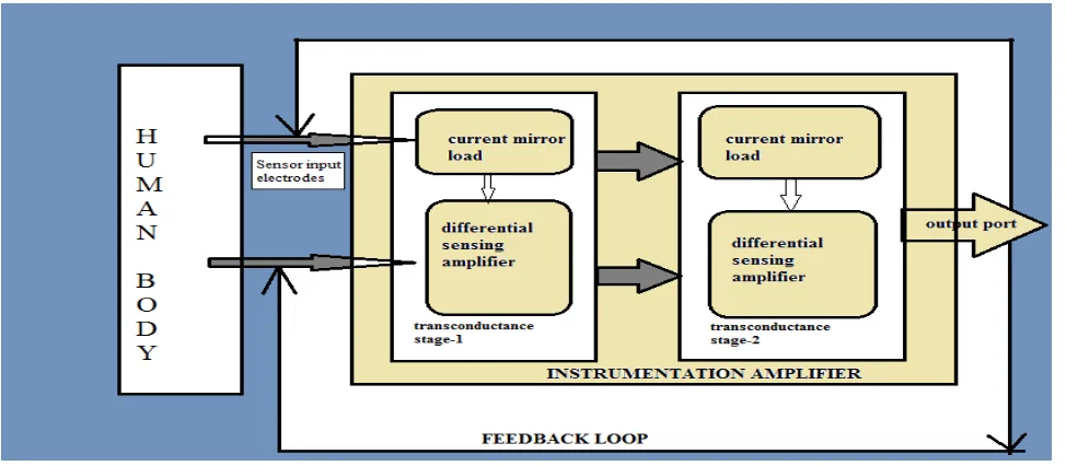
III.BLOCK DIAGRAM OF PROPOSED WORK
Fig 3: Block diagram of the proposed IA
to detect even micro-voltage signal in the presence of milli-voltage common mode signal; which is a challenging task. So a high input impedance IA is required. Sensing input is fed to a transconducting stage with local current feedback. Local current feedback has various advantages over resistor feedback in terms of balancing and degree of matching.
Both the direct and indirect current feedback IA topologies are subjected to a number of parasitic poles associated with each of the stages around the loop. As a result, this complicates the frequency compensation and poses a limitation on high-frequency operation. On the contrary, in the local current feedback IA topology, each local loop contains a smaller number of internal parasitic poles and thus, this topology potentially offers a higher operating BW for a given current consumption. For these reasons we have chosen the local current feedback IA topology implemented with a current mirror load (drain load) in the input transconductor.
Sensing differential amplifier will sense the small signal and provide it a sufficient gain by matching the drain currents of both the transconductance stages. Current mirror load is provided at each stage to provide better stability by feedback and thus reduced the parasitic. It is also insensitive towards offset voltages where resistive load are sensitive towards offset voltages.
IV.MATHEMATICAL CALCULATIONS OF IA
Fig 4: Equivalent model of transconductance stage.
A set of equations governing the common-mode gain characteristics of the IA can be formulated by first applying KCL at the drain and source terminals of the input stage. Next, to obtain the equations for the common-mode signal responses, we take the sum between the drain equations at d1 and d2, and between the source equations at s1 and s2. Similarly, toobtain the equation for the differential-mode signal response, we take the difference between the drain equations at d1 and d2, and between the source equations at s1 and s2. These sum and difference equations of the KCL node equations enable us to understand the underlying mechanism that leads to a finite common-mode gain due to component mismatches. In particular, the sum equations will be employed to determine the common-mode voltages of the IA. If there are mismatches, the common-mode voltages will give rise to differential current injections into the circuit. Subsequently, the difference equations will be employed to determine the circuit response, and hence the finite common-mode gain of the IA can be computed.
Applying KCL at node s1 in fig 2, we get;
SCs2 * Vs2 + Gs2 * Vs2 + Gmi2 * Vs2 – Gds2 * Vd2 + Gds2 * Vs2 = Gmi2 * Vic2 + SCgs2 * Vic2 ...eq(2)
As the two MOSes are identical therefore their internal parameters are also equal. For common mode gain the circuit is open circuited at the midway of R1 resistor . hence removing the suffixes 1 and 2. Adding equation 1 and 2 (also for common mode gain Vs = [Vs1+Vs2]/2) ...eq(3) we get,
2[SCs * Vs + Gs * Vs + Gmi * Vs – Gds * Vd + Gds * Vs] = 2[Gmi * Vic + SCgs * Vic] ...eq(4) [SCs * Vs + Gs * Vs + Gmi * Vs – Gds * Vd + Gds * Vs] = [Gmi * Vic + SCgs * Vic] ...eq(5) Taking Vs common from LHS and Vic from RHS;
[SCs + Gs + Gmi – Gds + Gds] * Vs = [Gmi + SCgs] * Vic ...eq(6) Applying KCL at node d1 in fig2, we get;
Gds1 * Vs1 + Gmi1 * Vs1 – Gmd1 * Vd1 - Gds1 * Vd1 – SCgd1 * Vd1 – SCd1 * Vd1 = Gmi1 * Vic1 – SCgd1 * Vic1 ...eq(7) Applying KCL at node d2 in fig 2, we get;
Gds2 * Vs2 + Gmi2 * Vs2 – Gmd2 * Vd2 - Gds2 * Vd2 – SCgd2 * Vd2 – SCd2 * Vd2 = Gmi2 * Vic2 – SCgd2 * Vic2 ...eq(8) As the two MOSes are identical therefore their internal parameters are also equal. For common mode gain the circuit is open circuited at the midway of R1 resistor . hence removing the suffixes 1 and 2. Adding equation 1 and 2 (also for common mode gain Vd = [Vd1+Vd2]/2) ...eq(9) we get,
2[Gds * Vs + Gmi * Vs – Gmd * Vd - Gds * Vd – SCgd * Vd – SCd * Vd] = 2[Gmi * Vic – SCgd * Vic] ...eq(10)
[Gds * Vs + Gmi * Vs – Gmd * Vd - Gds * Vd – SCgd * Vd – SCd * Vd] = [Gmi * Vic – SCgd * Vic]...eq(11) Taking Vd common from LHS and Vic from RHS;
[Gds + Gmi] * Vs –[ Gmd - Gds – SCgd – SCd] * Vd = [Gmi – SCgd ]* Vic ...eq(12)
From eq(6) and (12) we get the two unknown and two equation , we can easily calculate Vd and Vs from here and hence common-mode gain.
Now moving towards differential gain we have to consider the in between resistor R1 i.e short circuited , considering dVd = dVd1 – dVd2...eq(13), dVs = Vs1 – Vs2...eq(14) and the feedback current Ifs.
Applying KCL at node s1 and s2, we get;
[Gmi * Vs1 + 2/R1 * Vs1 + Gds * Vs1 + Gs * Vs1 + SCgs * Vs1 + SCs * Vs1- Gmi * Vs2 + 2/R1 * Vs2 + Gds * Vs2 + Gs * Vs2 + SCgs * Vs2 + SCs * Vs2]/2 – Gds * (Vd1) + Gds * (Vd2) – Ifs = Gds * (Vd - Vs) – Gmi * (Vic - Vs) + Gs* Vs + SCgs * (Vic - Vs) + SCs* Vs...eq(15) From (13) and (14) we get;
(Gmi + 2/R1 + Gds + Gs + SCgs + SCs) * dVs/2 – Gds * (dVd/2) – Ifs = Gds * (Vd - Vs) – Gmi * (Vic - Vs) + Gs* Vs + SCgs * (Vic - Vs) + SCs* Vs...eq(16)
Applying KCL at node d1 and d2, we get;
[Gmi * Vs1- Gmi * Vs2 + Gds * Vs1 – Gds * Vs2]/2 - [Gds * Vd1 + SCd * Vd1 + SCgd * Vd1 - Gds * Vd2 - SCd * Vd2 + SCgd* Vd2]/2 – Ifd = Gmi (Vic - Vs) + Gds (Vd - Vs) + Gmd * Vd – SCgd * (Vic - Vd) + SCd * Vd...eq(17) From eq (13) and (14) we get;
(Gmi + Gds) * dVs/2 – (Gds + SCgd + SCd) * dVd/2 – ifd = Gmi (Vic - Vs) + Gds (Vd - Vs) + Gmd * Vd – SCgd * (Vic - Vd) + SCd * Vd...eq(18) Hence from equation 16 and 18 we can easily calculate the differential gain. Following this, we have dVd = Vd1-Vd2~0, i.e., a differential-mode virtual ground condition.
respectively the total capacitances of the source and drain terminals, ifs is the differential feedback current, Gmd is the transconductance of the drain transistors.
V. DESIGNING OF INSTRUMENTATION AMPLIFIERS: ANALYSIS
We have designed three different IA in this paper. Fig 5 shows the direct current feedback instrumentation amplifier. It is often used in low power biomedical applications. Transistors connected to the input terminals and resistors in between them form a voltage to current converter with a transconductance of 1/R1. Another voltage to current converter is formed between bottom two transistor pairs with a transconductance of 1/R2, which provides feedback from the output.
Fig 5: schematic diagram of direct current feedback IA
The gain of the current feedback IA is given by the mathematical expression:
{(Vout-Vref)/Vin} = {(R3 + R4)/R4}(G1/G2) where G1 is the transconductance composed of M1, M2 and R1, G2 is the transconductance composed of M3, M4 and R2. In this circuit M1, M2 are always biased at the same drain current I, while transistors M3, M4 carry a signal dependent drain current. This difference in the bias currents can be a source of nonlinearity. The cascading of two voltage to current converters decreases the input common mode voltage range.
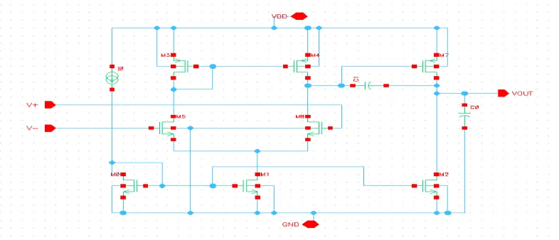
Fig 6 shows the schematic diagram of two stage opamp which is used in direct and indirect feedback instrumentation amplifiers to provide large loop gain. 2 stage opamp provides a gain of 50 dB; consists of two capacitors of C0 and C1 where C0 = 8pF and C1 = 3pF. Total of 5 NMOS and 3 PMOS are placed, a dc current source is provided at the current mirror load to maintain the drain current of differential amplifier stage, also at last voltage buffer is used.
Fig 7 shows the indirect current feedback instrumentation amplifier. The gain equation is same as in direct one, {(Vout-Vref)/Vin} = {(R3 + R4)/R4}(G1/G2). In this approach the transistors M1 and M2, M3 and M4 carry a signal dependent drain current, thereby eliminating this source of non-linearity, while the minimum supply voltage and input voltage ranges are also relaxed. Here input common mode voltage and reference common mode voltage are independent with each other. So to achieve this we have to give more current dissipation. Hence it is used where good linearity and gain accuracy is required.
Fig 7: schematic diagram of indirect current feedback IA
Fig 8 & 9 are the schematic of proposed instrumentation amplifier with given specification, sizes of MOS, resistors, capacitors. It is designed in virtuoso design environment, using 180nm technology. Library files included is UMC18CMOS technology files, all the components are placed from the same library files. Three terminal resistors and capacitors are used and 3rd terminal is connected to VDD as body is of P-type. Total of 33 MOS with 10 resistors and 2 capacitors are required with a power supply of 1.8V.
Fig 8: test bench simulation with resistor banks for R0 & R1
There are basically two approaches for designing of an IA. One is resistive feedback {3 opamp circuit of IA [11]} and second approach is current feedback [16]. Here we are using current feedback because of few reasons and disadvantages of resistive feedback circuits like CMRR is reduced by degree of matching of the resistors but in current feedback there is perfect isolation between input and output and balancing technique is also achieved.
In local current feedback IA there are few number of internal parasitic poles and thus this circuit offers a higher 3dB frequency and operating bandwidth. While in case of other feedback such as direct and indirect feedback [4] there are more number of poles associated with each stage and hence operating bandwidth reduces. Fig 1 current feedback is implemented with current mirror load transconductor [7]. One positive point of current mirror is insensitive to input offset voltage of loop amplifier. It also provides a large loop gain due to its higher impedence output node.
Ultimately sensing amplifier has relatively low gain and which will provide better stability, high bandwidth, hence power-area efficient.
Table 1: UMC18_CMOS technology components used
S.NO DNFTCMOS USED DRAIN CURRENT REGION OF OPERATION W/L RATIO 1. M1 NMOS 56.74μA 2(SATURATION) 2μm/180nm 2. M2 NMOS 22.06μA 2 540nm/180nm
3. M3 NMOS 75.01μA 2 3μm/180nm 4. M4 NMOS 14.99μA 2 3μm/180nm 5. M5 NMOS 1.79μA 2 240nm/240nm
6. M6 NMOS 1.79μA 2 240nm/540nm
7. M7 NMOS 1.55μA 2 240nm/540nm
8. M8 NMOS 18μA 2 2μm/180nm 9. M9 NMOS 10.37μA 2 500nm/180nm
10. M2B NMOS(capacitor) 0A(Shorted) 1(LINEAR) 240nm/180nm
11. M11 PMOS -13.33μA 2 10μm/180nm 12. M12 PMOS -13.33μA 2 10μm/180nm 13. M13 PMOS -75.07μA 2 10μm/180nm 14. M14 PMOS -1.79μA 2 10μm/180nm 15. M15 PMOS -1.79μA 2 1μm/180nm 16. M16 PMOS -12.34μA 2 10μm/180nm 17. M17 PMOS -1.79μA 2 240nm/180nm
18. M18 PMOS -1.55μA 1 240nm/540nm
19. M19 PMOS -18μA 1 1μm/180nm 20. M20 PMOS -10.37μA 2 5μm/180nm 21. M21 PMOS -10.37μA 2 5μm/180nm 22. M22 PMOS -5.41μA 2 1μm/180nm 23. M23 PMOS -58.74μA 1 5μm/180nm 24. M24 PMOS -22.06μA 1 5μm/180nm 25. M25 NMOS 10.37μA 2 540nm/180nm
VI.SIMULATED RESULTS OF IA
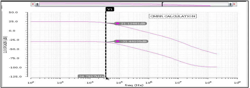
CMRR is defined as the ratio of differential gain to common mode gain. (CMRR = Ad/Ac), fig 10 shows Ad and Ac but they are in dB so we have to use logarithms identity rules here. Therefore CMRR = Ad-[-Ac]
Fig 10: CMRR analysis and bandwidth of direct feedback IA
From fig 10 CMRR at 34.7857 KHz cut-off frequency = 21.12-[-31.46]. Hence CMRR = 52.58 dB, which is comparatively low for a imaging amplifier. In order to achieve a high rejection over common mode signals CMRR should be above 80 dB. However power dissipation for this IA is minimum (222 micro-watts); hence it is used in low power applications where low power is the fundamental aim of the device.
Fig 11: CMRR analysis and bandwidth of indirect feedback IA
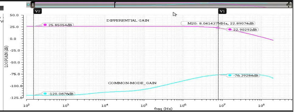
Fig11 shows CMRR at 47.52 KHz cut-off frequency = 35.77-[-27.844]. Hence CMRR = 63.614 dB, which is also comparatively low for an imaging amplifier. In order to achieve a high rejection over common mode signals CMRR should be above 80 dB. Fig 12 shows CMRR analysis of the proposed IA at R0 = 400 ohms and R1 = 20 K ohms and cut-off frequency of 8 MHz.
Fig 12: CMRR analysis and bandwidth of proposed variable-gain IA
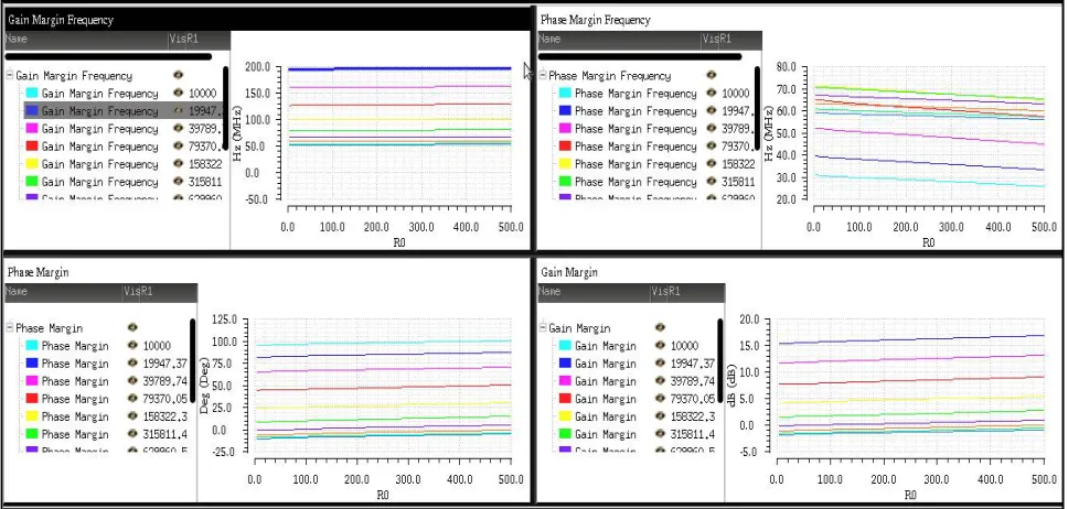
Fig 13: stability summary of the proposed variable-gain IA
Hence, gain of the IA would be the same as earlier one at higher temperature ranges also. This is a necessity of the circuit to be fabricated, which will provide better stability to the amplifiers that are going to work in noisy and tough conditions. Fig 13 shows the stability criterion in terms of frequency response, where gain margin and phase margin should be positive. Above 5 dB of GM and for the PM of above 10 degree, the system will be stable. From the figure it can be conclude that for different R0 and R1 values; Wpc(phase cross-over frequency) > Wgc(gain cross-over frequency) and GM,PM are positive that indicates the system is stable enough, provided the loop gain should be high, MOS transistors operates in saturation region and bandwidth of the IA is enough for the requirement of operation. Graph clearly shows that for which value of R0 and R1 the system is unstable (That is GM & PM is negative).
Fig 14: variable gain v/s frequency curve of variable-gain IA
response. Its slew rate should be infinite ideally. Slew rate is defined as the ratio of change in output voltage with respect to time. Here it is 38.3V/μS.
Fig 15: IIP3 analysis of the proposed variable-gain IA
For good linearity, the maximum differential input ranges is restricted to the value 2*Is*R1. Where current here is drain
current of source transistor 22.04μA, voltage is therefore 2.2mv and above this harmonic distortion may occur. IIP3 analysis is also shown below fig 15 of 37.93dBm which is good enough. Hence high degree of linearity is obtained.
The intercept point is obtained graphically by plotting the output power versus the input power both on logarithmic scales (e.g., decibels) shown in fig 15. Two curves are drawn; one for the linearly amplified signal at an input tone frequency, one for a nonlinear product.Both curves are extended with straight lines of slope 1 and n (3 for a third-order intercept point). The point where the curves intersect is the intercept point. It can be read off from the input or output power axis, leading to input or output intercept point, respectively (IIP3/OIP3).
When comparing systems or devices for linearity, then, a higher intercept point is better. This device with an input-referred third-order intercept point of 37.82dBm is driven with a test signal of −30 dBm. This power is 67.82 dB below the intercept point; therefore nonlinear products will appear at approximately 2x67.82 dB below the test signal power at the device output (in other words, 3×67.82 dB below the output-referred third-order intercept point).
Fig 16: noise response of input and output ports of proposed IA
noise effect is low at both the ports; hence we can neglect its effect easily in the results. There is circuit noise internal to the subcomponents in the front end. This noise will add on to the AWGN, cause interference, and further degrade the SNR. Circuit noise is associated with the electrical components that build the subcomponents, such as resistors and MOS transistors.
Fig 17 is the layout of IA with minimum area with no DRC errors. Resistors are placed apart from power supply in order to achieve low mismatches and minimum resistive layers are used with proper design rules specifications. As circuit designers we must carefully consider how to draw layout for critical/sensitive parts of the circuit in order to get robust and predictable performance.
Fig 17: Layout of the proposed variable gain IA
Table 2: CMRR summary of instrumentation amplifiers at their cutoff frequencies
S.NO INSTRUMENTATION AMPS COMMON-MODE GAIN DIFF.GAIN CMRR 01. Direct current feedback IA -30 dB 25 dB 55 dB
02. Indirect current feedback IA -27 dB 36 dB 63 dB
03. Variable gain IA(local current feedback) -76 dB 24 dB 100 dB Table 3: Results of proposed variable gain IA
VII. CONCLUSION AND FUTURE WORK
We have presented a variable gain amplifier with two resistor banks, which will provide variable gain to the IA. Different values of R0 and R1 are considered to obtain the variable gain from 15 to 50 dB. Stability criterion is kept in mind while designing a high bandwidth IA of 8MHz. It gives the information about the stability of the circuit. With varying gain we have to trade off between gain and stability. Other than this it is giving a 100 dB CMRR at the high
S.NO PARAMETERS SPECIFICATIONS RESULTS OBTAINED 1. Process technology - 180nm technology
2. CMRR >80 dB at 2MHz 100dB at 8.03MHz
3. Differential gain >30 dB 15-45 dB
4. Common-mode gain - -76 dB at 8.03MHz
5. Slew Rate >2V/μS 38.3V/μS 6. Area Minimum as possible 0.000985mm-sq
7. Power dissipation <1mw 567μw 8. Bandwidth ~2 to 10 MHz 8.03 MHz
9. Supply voltage 1.8V 1.8V
10. Input referred noise <20μV 9.77μV 11. Gain Margin Should be positive >5 dB
12. Phase Margin Should be positive >10 degrees
13. Wgc - Varies as per diff. gain
frequency of 8MHz with low power dissipation of 567 μw, low input referred noise and minimum area of 0.000985 mm-square. This local current feedback variable gain IA is compared with two IA (Current feedback IA and indirect current feedback IA) and is comparatively more stable, higher CMRR value. This amplifier is a boon to bioimpedance imaging, EIT and other bio-medical applications.
REFERENCES
[1]. B. D.Miller and R. L. Sample, “Instrumentation amplifier IC designed for oxygen sensor interface requirements,” IEEE J. Solid-State Circuits, vol. 16, no. 6, pp. 677–681, Dec. 1981.
[2]. V. Schaffer, M. F. Snoeij, M. V. Ivanov, and D. T. Trifonov, “A 36 V programmable instrumentation amplifier with sub-20 V offset and a CMRR in excess of 120 dB at all gain settings,” IEEE J. Solid-StateCircuits, vol. 44, no. 7, pp. 2036–2046, Jul. 2009.
[3]. J.-M. Redouté and M. Steyaert, “An instrumentation amplifier input circuit with a high immunity to EMI,” in Proc. 2008 Int. Symp. Electromagn.Compatibility—EMC Eur., Hamburg, Germany, Sep. 2008, pp. 1–6.
[4]. J. F. Witte, J. H. Huijsing, and K. A. A. Makinwa, “A current-feedback instrumentation amplifier with 5 V offset for bidirectional highside current-sensing,” IEEE J. Solid-State Circuits, vol. 43, no. 12, pp. 2769–2775, Dec. 2008.
[5]. M. Rahal and A. Demosthenous, “A synchronous chopping demodulator and implementation for high-frequency inductive position sensors,”
IEEE Trans. Instrum.Meas., vol. 58, no. 10, pp. 3693–3701,Oct. 2009.
[6]. M. S. J. Steyaert, W. M. C. Sansen, and C. Zhongyuan, “A micropower low-noise monolithic instrumentation amplifier for medical purposes,”
IEEE J. Solid-State Circuits, vol. SC-22, no. 6, pp. 1163–1168, Dec. 1987.
[7]. R. Martins, S. Selberherr, and F. A. Vaz, “A CMOS IC for portable EEG acquisition systems,” IEEE Trans. Instrum. Meas., vol. 47, no. 5, pp. 1191–1196, Oct. 1998.
[8]. C.-J. Yen, W.-Y. Chung, and M. C. Chi, “Micro-power low-offset instrumentation amplifier IC design for biomedical system applications,”
IEEE Trans. Circuits Syst. I, Reg. Papers, vol. 51, no. 4, pp. 691–699, Apr. 2004.
[9]. K. A. Ng and P. K. Chan, “A CMOS analog front-end IC for portable EEG/ECG monitoring applications,” IEEE Trans. Circuits Syst. I, Reg. Papers, vol. 52, no. 11, pp. 2335–2347, Nov. 2005.
[10]. R. F. Yazicioglu, P. Merken, R. Puers, and C. V. Hoof, “A 60 W 60 nV Hz readout front-end for portable biopotential acquisition systems,”
IEEE J. Solid-State Circuits, vol. 42, no. 5, pp. 1100–1110, May 2007.
[11]. C.-C. Wang, C.-C. Huang, J.-S. Liou, Y.-J. Ciou, I-Y. Huang, C.-P. Li, Y.-C. Lee, and W.-J.Wu, “A mini-invasive long-term bladder urine pressure measurement ASIC and system,” IEEE Trans. Biomed. CircuitsSyst., vol. 2, no. 1, pp. 44–49, Mar. 2008.
[12]. H. Hong, M. Rahal, A. Demosthenous, and R. Bayford, “Comparison of a new integrated current source with the modified Howland circuit for EIT applications,” Physiol. Meas., vol. 30, no. 10, pp. 999–1007, Oct. 2009.
[13] M. Rahal, A. Demosthenous, and R. Bayford, “An integrated common mode feedback topology for multi-frequency bioimpedance imaging,” in
Proc. 35th Eur. Solid-State Circuits Conf. (ESSCIRC’09), Athens, Greece, pp. 416–419.
[14]. R. Bayford, “Bioimpedance tomography (electrical impedance tomography),” Annu. Rev. Biomed. Eng., vol. 8, pp. 63–91, Aug. 2006. [15]. S. Grimns and Ø. G. Martinsen, Bioimpedance & Bioelectricity Basics. London, U.K.: Academic, 2000.
[16]. Analogue IC Design: The Current-Mode Approach, C. Toumazou, F. J. Lidgey, and D. G. Haigh, Eds. London, U.K.: Peter Peregrinus Ltd., 1990, ch. 16, pp. 569–595.