Available online:
http://edupediapublications.org/journals/index.php/IJR/
P a g e | 3171Dynamic Composite Resistive Switching
Characteristics of Multiple Interconnected
Memristors
N Khadar Basha
1& T Ramashri
21
Department of ECE, SVUCE, Andhra Pradesh, India
2
Professor, Department of ECE, SVUCE, Andhra Pradesh, India.
Abstract:
In novel technologies, the memristive technology is most promising one it, fulfils nanoscale requirements - scaling down to less than 10 nm, low power consumption, low energy switching characteristics and nonvolatile nature. Memristor became one of the basic fundamental building unit for designing logic circuits and memory devices. Memristive devices are envisioned to provide new functionalities at the nanoscale based on the possibility to tune their resistivity continuously. More researchers focusing only the modelling of the memristor and a very few papers published on the composite behavior of memristors but not completely explained. Important efforts are still needed to understand the switching mechanism. In this paper, we analysis the composite memristive voltage-dependent switching behavior by considering memristor as a single structural element. Serial and parallel connected memristors composite characteristics are investigated because of its various application of as basic memory element in crossbar architectures. Complementary Resistive Switch (CRS) and Anti-parallel Resistive Switch (ARS) are the composite memristors use in logic circuit design and memory circuit elements.
Keywords
switching characteristics; composite; memristive;
Ant-parallel Resistive Switch; Complementary
Resistive Switch;
1.
Introduction
Memristor is the most important element due to its ubiquity and its usage in diverse areas of science, engineering and biotechnology. Resistive switching mechanism of memristor plays major role in
designing non-volatile memory [1]-[2] and
reconfigurable circuits and architectures [3]-[6]. Memristors are primarily used in computations due to its dynamic resistance and the interconnected memristors improve efficiency [7]. The switching
characteristics of memristor are studied in [8]-[9] and multiple interconnected memristor are studied in [10]. The composite memristors are used to design programmable state devices. Memristor consist of two terminals with two states, Low Resistance State (LRS) considered as Logic ‘1’ or ON state and High Resistance State (HRS) represents logic ‘0’ or OFF state of memristor [11]. As shown in figure 1 the memristor is a two terminal device consists of two layers of oxide region, top layer is doped with
oxygen vacancy it act as conductor. The oxygen
Figure. 1 (a) Memristor Symbol (b) Physical Structure of Memristor (c) ON State Memristor (d) OFF State Memristor
Available online:
http://edupediapublications.org/journals/index.php/IJR/
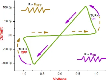
P a g e | 3172and the layer appears as undoped, hence it has high resistance. This state is called OFF state of memristor or High Resistance State (HRS) as shown in figure 1(d). Depends on the applied voltage and forward/reverse biasing, the transition between this states can be changed, the memristance switching range is in between LRS and HRS, i.e LRS<Rmem<HRS and this range is controlled by SET (Vths) and RESET (Vthr) threshold voltages in voltage controlled devices. Once the memristance reaches it boundary its value cannot change further. The memristance depends on the how much voltage and time duration of applied voltage to the memristor terminals. It retains it memristance without continues applying voltage. When bipolar voltage is applied then the memristor exhibit hysteresis curve in V-I characteristics. This pinched hysteresis is fingerprint for memristor. When the input voltage is kept in the operating region (Vin < |Vths| and |Vthr|), the device stays in its current state. Setting the input voltage outside of the operation region, past a threshold value, the device enters into the switching region, (Vin > |Vths| and |VTR|), with a subsequent changing
of its state (ON to OFF, or OFF to ON) as shown in figure 2.
Figure. 2 Switching behavior of memristor
2.
Switching Dynamics of Single
Memristor
The electrical characteristics of memristor are difficult to understand due to the nonlinear behavior characteristics of flux and charge, before designing different memristor circuit topologies, it is necessary to understand the dynamic switching characteristics of single memristor, series and parallel connected memristors under different initial states under forward/reverse biased condition.
SPICE model of memristor with threshold is important for designing complementary resistive switches, crossbar architectures but very few models are available with threshold and they also designed with fixed threshold voltage which are applicable for
only particular input signals [12]-[13]. The spice model with threshold switching characteristics which we designed is works fine with different threshold
voltages, over wide range of input voltage and frequencies [14].
Figure. 3 (a) A 3V Triangular wave signal applied to memristor. (b) Current through the memristor. (c) Change in memristance according to the input signal.
(d) V-I characteristics of memristor.
Now we start analysis with single memristor by applying 3V triangular signal to the memristor. The spice model of memristor we set The SET voltage (Vths) and the RESET voltage (Vthr) are 0.7V and -0.7V respectively. The results are observed as shown in figure 2. Initially there is no current flow through memristor, the current starts when the applied voltage greater than Vths and again the device stops current when the applied voltage is |Vthr| as shown in figure 3(b) and the corresponding resistance change is observed in the figure 3(c), the resistance is low between the SET and RESET interval of the applied voltage. The V-I characteristics of memristor is important to one to analysis the memristor. At origin of XY graph voltage and current are zero, as the voltage is increases then no significant current change is observed below Vths. When the voltage is in between Vths and |Vthr|, then the current change according to the applied voltage (ON state) i.e. the device act as linear device in this region. When the applied voltage is greater than the |Vthr| then there is no current flows and once again the device is in OFF state as shown in figure 3(d).
The initial state of memristor plays important role along with biasing in the analysis of memristive circuit design. Hence we start analysis with single memristor under forward/reverse biased voltage source of 3V triangular wave signal with initial ON/OFF state as shown in figure 4. We study the fallowing dynamic characteristics of memristor:
0.0 0.5 1.0 1.5 2.0
-1.5 -1.0 -0.5 0.0 0.5 1.0 1.5
0.0 0.5 1.0 1.5 2.0
-400.0µ -200.0µ 0.0 200.0µ 400.0µ 600.0µ 800.0µ
0.0 0.5 1.0 1.5 2.0
0.0 50.0k 100.0k 150.0k 200.0k 250.0k
-1.5 -1.0 -0.5 0.0 0.5 1.0 1.5
-400.0µ -200.0µ 0.0 200.0µ 400.0µ 600.0µ 800.0µ
Voltage
Time a
Current
Time b
Memristanc
e
Time c
Current
Available online:
http://edupediapublications.org/journals/index.php/IJR/
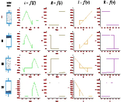
P a g e | 3173Current (I)-Time, Memristance (R)-Time, Current (I)-Voltage (V) and Memristance (R)-Voltage (V) as shown in figure 4. The first column of the figure represent the initial state of memristor as ON state or OFF state as explained in figure 1(c) and 1(d), this is done by using initial value of memristance is minimum and maximum respectively in the spice model [3]. The second and third columns represent change in current and memristance as a function of
time respectively. The third and fourth column represent current and resistance as a function of voltage respectively.
Figure. 4 Switching dynamics of single memristor under different biasing conditions and different initial
states.
As shown in figure 4(I), the memristor is initially in ON state and the 3V triangular wave source is forward biased, hence the current pass through the device in certain interval of time and stops at which time the applied voltage reaches Vthr as shown in figure 4(a). The initial memristance of device is low because the device is in ON state and the device change its resistance state at the time of the applied voltage is equal to RESET voltage as shown in figure 4(b). In the V-I characteristics of memristor as shown in figure 4(c), at the origin both voltage and current are zero, as the voltage is increases then the current is also increases regardless of Vths because the device is initially in ON state and as the voltage is decreases its current is also decreases until the voltage reaches Vthr, hence in ON state the device act as linear device until the applied voltage reaches Vthr. When the applied voltage reaches then the current becomes less and the device transits to OFF state. As shown in figure 4(d) as the voltage increases then the voltage then the resistance is less because initially the device is in ON state and has low resistance state and no further resistance is decreases. When the voltage is equal to Vthr then the resistance of memristor is increases to maximum and
then the voltage increases or decreases it resistance is maximum. In overall when the memristor is initially in ON state and forward biased then the Vths only cable to change the state of memristor.
A 3V triangular wave source is connected in forward biased to initially OFF state memristor, the characteristics are observed as shown in figure 4(II). The current flows through the device only a particular interval of time where the applied voltage is in between the threshold voltages, no current flows through device above the threshold ranges as shown in figure 4(e). The memristance also low at the time interval of that the current flow through the device as shown in figure 4(f). The hysteresis curve as shown in figure 4(g), as the voltage increases, upto Vths there is very less current flow. Further increases the voltage, the current also sharply increases and then according to voltage the current changes. When the applied voltage reaches Vthr then the current is again low. The voltage-resistance curve as shown in figure 4(h), due to the OFF state of memristor the initially it has high resistance, when the voltage reaches Vths then the resistance is low as the voltage increases the resistance is low and as the voltage decreases then the current resistance is low until the voltage reaches the Vthr and gain the resistance increases. From above analysis, when the memristor is initially in OFF state and forward biased, then to turn ON and turn OFF the device Vths and Vthr plays major role respectively.
Available online:
http://edupediapublications.org/journals/index.php/IJR/
P a g e | 3174A 3V triangular wave source is reversed biased to the initial OFF state memristor, the characteristics are observed as shown in figure 4(IV). Initially there is no current flow the device due to OFF state and no state occurs until the time interval of voltage is equal to reset voltage as shown in figure 4(m). The memristor memristance can change an interval of time at which the applied voltage is equal to the Vthr as shown in figure 4(n). The V-I characteristics of this condition are observed as shown in figure 4(o), as the voltage increases the no current change and when the voltage in decreases again the current change is less upto the voltage is equal to Vthr, then after the current changes according to the applied voltage. As shown in figure 4(p) initially the resistance is high as the voltage increases there is no state change occur, when the voltage is decreases the resistance is high until the voltage is equal to Vthr, then after the resistance is low.
3.
Switching characteristics of series
connected memristors
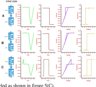
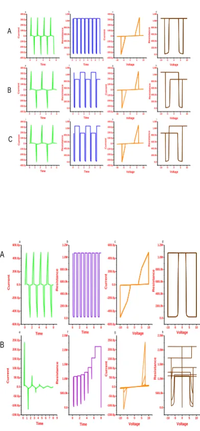
Let start analysis with the simplest structure which consists of two memristors only. Both memristors are connected in series and 3V AC triangular voltage signal applied. Based on the initial state/condition of memristors, three possible combinations ON/ON, ON/OFF and OFF/OFF are examined. Memristors are connected in series, due to its internal resistance of memristors the voltage is divided like voltage divider circuit.
As shown in the above figure 5(A), both memristors are initially off state, the voltage is divided equally because of equal internal resistances and when the voltage exceeds threshold voltage Vths (1.4V) then both will be turned ON or switch their internal states. When the applied voltage is greater than composite threshold voltage of memristors then they toggle states as shown in figure 5(a-d). In a series connected memristors, the total or composite threshold voltage is the sum to their individual threshold voltages, i.e. If n is the number of memristors connected in series then their composite
threshold is , and total composite
memristance
The memristors are initialized as OFF/ON as shown in figure 5(C). The state change of the upper memristor occurs much quicker at lower voltages because of the high ratio of memristance at the boundary. The lower memristor remains same in that
state as shown in figure 5(g). At RESET voltages both devices switch its stages from ON to OFF state simultaneously.
In the case of memristors are initialized as ON/ON, during positive applied voltage the states cannot change. By applying RESET voltage the state
toggled as shown in figure 5(C).
Figure. 5 Characteristics of forward biased series connected memristors.
Similar to forward biased condition, we examine the composite memristors behavior under reverse bias as shown in figure 6. Initially both memristor are set in OFF condition as shown in figure 6(A), for the positive half cycle, they don’t effect because they already in HRS (max resistance state) so there is no effect. Both devices switch states only when the applied voltage is less than the composite RESET voltages (greater than the |Vthr|). When the memristor are initially in OFF/ON condition for the positive half cycle, second memristor switches from on state to off state hence state change occurs very fast and OFF to ON memristance ratio increases. However, owing to the high memristance ratio, the corresponding voltage drop on this device never exceeds its RESET threshold; thus the total memristance remains equal to ROFF + RON ≈ ROFF. As shown in figure 6(C) the composite serial reversed biased memristors characteristics are opposite behavior of ON/ON forward biased condition as shown in figure 5(C).
We may conclude from all above observations that when the memristor are connected with the same polarities in either forward or reverse bias, then their behavior is same as the single memristor but the switching properties are composite.
0.00.51.01.52.0
-800.0µ -700.0µ -600.0µ -500.0µ -400.0µ -300.0µ -200.0µ -100.0µ 0.0 100.0µ
0.00.51.01.52.0
0 100k 200k 300k 400k 500k
-3-2-10123
-800.0µ -700.0µ -600.0µ -500.0µ -400.0µ -300.0µ -200.0µ -100.0µ 0.0 100.0µ
-3-2-10123
0 100k 200k 300k 400k 500k
0.00.51.01.52.0
-800.0µ -700.0µ -600.0µ -500.0µ -400.0µ -300.0µ -200.0µ -100.0µ 0.0 100.0µ
0.00.51.01.52.0
0.0 50.0k 100.0k 150.0k 200.0k 250.0k
-3-2-10123
-800.0µ -700.0µ -600.0µ -500.0µ -400.0µ -300.0µ -200.0µ -100.0µ 0.0 100.0µ
-3-2-10123
0.0 50.0k 100.0k 150.0k 200.0k 250.0k
0.00.51.01.52.0
-800.0µ -600.0µ -400.0µ -200.0µ 0.0 200.0µ 400.0µ
0.00.51.01.52.0
0.0 50.0k 100.0k 150.0k 200.0k 250.0k
-3-2-10123
-800.0µ -600.0µ -400.0µ -200.0µ 0.0 200.0µ 400.0µ
-3-2-10123
0.0 50.0k 100.0k 150.0k 200.0k 250.0k
Cu
rr
en
t
Time
a
Res
is
tan
ce
Time
b
Cu
rr
en
t
Voltage
c
Res
is
tan
ce
Voltage
d
Cu
rr
en
t
Time
e
Res
is
tan
ce
Time
f
Cu
rr
en
t
Voltage
g
Res
is
tan
ce
Voltage
h
+ -+
-OFF
OFF
+ -+
-OFF
ON
+ -+
-ON
ON C B
Cu
rr
en
t
Time
i
Res
is
tan
ce
Time
j
Cu
rr
en
t
Voltage
k
Res
is
tan
ce
Voltage
l
Initial state
Available online:
http://edupediapublications.org/journals/index.php/IJR/
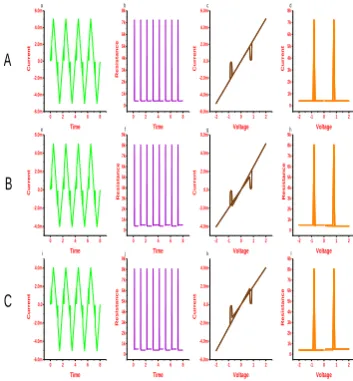
P a g e | 3175Now we observe the competitive memristor behavior by connecting in opposite polarities under the 3V AC triangular voltage sweep as shown in figure 7. Both devices are in opposite and initialized as OFF/OFF, for positive applied voltage, when it is greater than Vthr, the upper memristor switches ON and its memristance decreases, due to it a small voltage drop occurs which causes threshold voltage quickly and lower memristor remains in OFF condition. For the negative half cycle, lower memristor switches to low memristance state and the upper memristance from its intermediate state to high memristance state. The lower device starts switching first, initially it has high resistance, and draws almost all the applied voltage. The voltage drop decreases as its resistance reduces. At a particular point of time, voltage greater than the |Vthr|, switching process initiated. Subsequently, the upper memristor draws most of the entire applied voltage and its resistance increases, hence the voltage drop on the lower memristor never exceeds its threshold, due to this
process spike like structure form.
Figure. 6 Characteristics of reverse biased series connected memristors
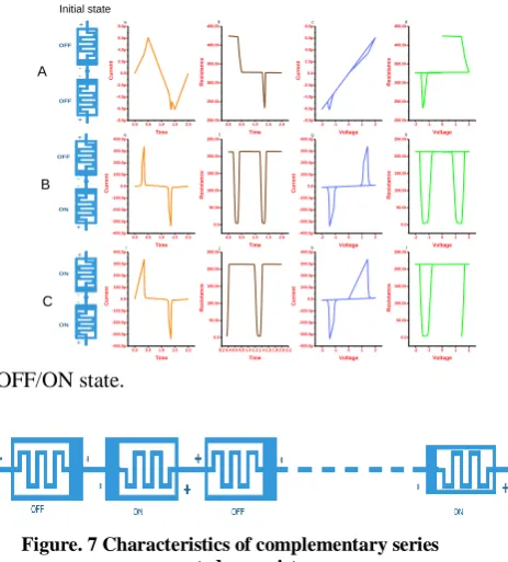
When both devices are initialized OFF/ON and reverse connected then acts as complementary devices, they change states exactly reciprocal way such that form composite V-I characteristics perfectly symmetrical. For positive voltage greater than Vths the upper memristor switches from OFF to ON state and lower memristor switches from ON to OFF state. Then after the memristors exhibit ohmic behavior within the composite threshold voltage, then goes back to the initial state. This functionality is useful for designing complementary resistive switch. In this case except for two voltage intervals, current is linear with voltage.
Both devices are initialized in ON/ON condition, i.e. low memristance stage, there is no state change
occurs until applied voltage reaches threshold voltage then the bottom memristor changes its state, the remaining operation is same as discussed earlier. After a complete sweep, the memristors are in
OFF/ON state.
Figure. 7 Characteristics of complementary series connected memristors
Figure. 8 Schematic of multi CRS circuits
We study the multiple CRS memristors connected in series connection under AC Triangular pulses as shown in the figure 8, the simulation results for ten memristor are observed as shown in figure 9. When the equal number of forward polarity memristors and reverse polarity memristors are connected in series then the circuits have more conduction interval along the voltage axis compared to the single CRS. When the applied voltage is more than the accumulated threshold voltage then only the state change occurs. Due to symmetrical distribution between the CRC memristors, the total composite memristance remains same as shown in figure 9(B).
The forward polarity memristors are greater and lesser than the reverse polarity memristors in CRS circuit the simulation results are observed as shown in figure 9(B) and 9(C) respectively. In the case of forward polarity memristors are greater than reverse polarity memristors, during the positive cycle, a shorter current pulse occurs and wider current pulse occurs during negative pulse of applied voltage. In this case of forward polarity memristor are lesser than reverse polarity memristor, a wider current pulse during positive cycle occurs and during the negative cycle a shorter current occurs. So from the above results, we observe that specific high current lobes can be widened or shorten by adding or removing forward or reverse polarity memristor and also we can change dominating duration.
0.00.51.0 1.52.0 -0.0004 -0.0002 0.0000 0.0002 0.0004 0.0006 0.0008
0.00.51.0 1.52.0 0 100k 200k 300k 400k 500k
-3-2-10123 -400.0µ -200.0µ 0.0 200.0µ 400.0µ 600.0µ 800.0µ
-3-2-10123 0 100k 200k 300k 400k 500k
0.00.51.0 1.52.0 -400.0µ -200.0µ 0.0 200.0µ 400.0µ 600.0µ 800.0µ
0.00.51.0 1.52.0 0.0 50.0k 100.0k 150.0k 200.0k 250.0k
-3-2-10123 -400.0µ -200.0µ 0.0 200.0µ 400.0µ 600.0µ 800.0µ
-3-2-10123 0.0 50.0k 100.0k 150.0k 200.0k 250.0k
0.00.51.0 1.52.0 -400.0µ -200.0µ 0.0 200.0µ 400.0µ 600.0µ 800.0µ
0.00.51.0 1.52.0 0.0 50.0k 100.0k 150.0k 200.0k 250.0k
-3-2-10123 -400.0µ -200.0µ 0.0 200.0µ 400.0µ 600.0µ 800.0µ
-3-2-10123 0.0 50.0k 100.0k 150.0k 200.0k 250.0k Cu rr ent Time a Res is tance Time b Cu rr ent Voltage c Res is tance Voltage d + -+ -OFF OFF + -+ -OFF ON + -+ -ON ON C B Cu rr ent Time e A Initial state Res is tance Time f C u rr e n t V(in1) g Res is tance Voltage h Cu rr ent Time i Res is tance Time j Cu rr ent Voltage k Res is tance Voltage l
0.00.51.01.52.0
-8.0µ -6.0µ -4.0µ -2.0µ 0.0 2.0µ 4.0µ 6.0µ 8.0µ
0.00.51.01.5 2.0
200.0k 250.0k 300.0k 350.0k 400.0k 450.0k
-2 -1 0 1 2
-8.0µ -6.0µ -4.0µ -2.0µ 0.0 2.0µ 4.0µ 6.0µ 8.0µ
-2 -1 0 1 2
200.0k 250.0k 300.0k 350.0k 400.0k 450.0k
0.00.51.01.52.0
-400.0µ -300.0µ -200.0µ -100.0µ 0.0 100.0µ 200.0µ 300.0µ 400.0µ
0.00.51.01.5 2.0
0.0 50.0k 100.0k 150.0k 200.0k 250.0k
-2 -1 0 1 2
-400.0µ -300.0µ -200.0µ -100.0µ 0.0 100.0µ 200.0µ 300.0µ 400.0µ
-2 -1 0 1 2
0.0 50.0k 100.0k 150.0k 200.0k 250.0k
0.00.51.01.52.0
-400.0µ -300.0µ -200.0µ -100.0µ 0.0 100.0µ 200.0µ 300.0µ 400.0µ
0.2 0.4 0.6 0.8 1.0 1.2 1.4 1.6 1.8 2.0 2.2 0.0 50.0k 100.0k 150.0k 200.0k 250.0k
-2 -1 0 1 2
-400.0µ -300.0µ -200.0µ -100.0µ 0.0 100.0µ 200.0µ 300.0µ 400.0µ
-2 -1 0 1 2
Available online:
http://edupediapublications.org/journals/index.php/IJR/
P a g e | 3176Figure 9. Characteristics of multiple CRS circuits.
Figure 10. Characteristics of Multi CRS Memristors with Asymmetric threshold voltages
Until now we analysis the characteristics with equal magnitude of SET and RESET voltages, when
we change the threshold voltages as Vthr|< |Vthr|. i.e
SET and RESET voltages are 0.5V and -1V respectively, then for both positive and negative voltage cycles, it creates a high conduction interval as shown in figure 10(A). When we change the SET and RESET voltage 1V and -0.5v respectively then the current reduced with increasing the time due to the shrinking of high conducting lobes as shown in figure 10(B).
4.
Switching Characteristics of Parallel
Connected Memristors
We e analyze the behavior of parallel connected
memristor by assuming memristor as a single structural element. In a parallel connection, the same voltage is present across all devices, hence ON resistance plays a major role, whereas in series connection the total resistance plays a major role in behavior and switching operation.
Figure 11. Characteristics of forward parallel connected memristors.
By considering a memristor as a smallest configuration element, the simulation results of two parallel interconnected memristors under AC triangular voltage is seen in figure 11. When two memristors are connected in forward polarity and initial states OFF/OFF then both memristors change their states to gather as shown in figure 11(A), so the I-V plots are same as single memristor IV plot, due to the parallel connection of memristors the total internal resistance of the circuit becomes half of initial states, hence the current becomes double and maintains the same memristance ratio. As shown in figure 10(B), one memristor is in HRS and another is LRS, due to the parallel connection for devices the total memristance is less than LRS memristance. Hence, for positive voltage less than the SET voltage, ON state device memristance reduces and another memristor switches from OFF to ON. Both of them switches states from ON to OFF for Vthr. When both devices are in LRS i.e. ON state, for positive voltage there is no effect on state because both are already in ON state shown in figure 11(C), for negative voltage their switching behavior is same as seen in the previous example.
0 2 4 6 8
-600.0µ -400.0µ -200.0µ 0.0 200.0µ 400.0µ 600.0µ
0 2 4 6 8
0.0 200.0k 400.0k 600.0k 800.0k 1.0M 1.2M
-10 -5 0 5 10
-600.0µ -400.0µ -200.0µ 0.0 200.0µ 400.0µ 600.0µ
-10 -5 0 5 10
0.0 200.0k 400.0k 600.0k 800.0k 1.0M 1.2M
0 1 2 3 4 5 6 7 8 9 -150.0µ -100.0µ -50.0µ 0.0 50.0µ 100.0µ 150.0µ 200.0µ 250.0µ
0 2 4 6 8
0.0 500.0k 1.0M 1.5M 2.0M 2.5M
-10 -5 0 5 10
-150.0µ -100.0µ -50.0µ 0.0 50.0µ 100.0µ 150.0µ 200.0µ 250.0µ
-10 -5 0 5 10
0.0 500.0k 1.0M 1.5M 2.0M 2.5M Current Time a A B Resistanc e Time b Voltage Current c Resistanc e Voltage d Time Current e Time Resistanc e f Voltage Current g Voltage Resistanc e h
0 2 4 6 8
-400.0µ -300.0µ -200.0µ -100.0µ 0.0 100.0µ 200.0µ 300.0µ 400.0µ
012345678 0.0 200.0k 400.0k 600.0k 800.0k 1.0M 1.2M
-10 -5 0 5 10 -400.0µ -300.0µ -200.0µ -100.0µ 0.0 100.0µ 200.0µ 300.0µ 400.0µ
-10 -5 0 5 10 0.0 200.0k 400.0k 600.0k 800.0k 1.0M 1.2M
0 1 2 3 4 5 -400.0µ -300.0µ -200.0µ -100.0µ 0.0 100.0µ 200.0µ 300.0µ 400.0µ
0 1 2 3 4 5 0.0 200.0k 400.0k 600.0k 800.0k 1.0M 1.2M
-10 -5 0 5 10 -400.0µ -300.0µ -200.0µ -100.0µ 0.0 100.0µ 200.0µ 300.0µ 400.0µ
-10 -5 0 5 10 0.0 200.0k 400.0k 600.0k 800.0k 1.0M 1.2M
0 1 2 3 4 5 -400.0µ -300.0µ -200.0µ -100.0µ 0.0 100.0µ 200.0µ 300.0µ 400.0µ
0 1 2 3 4 5 0.0 200.0k 400.0k 600.0k 800.0k 1.0M 1.2M
-10 -5 0 5 10 -400.0µ -300.0µ -200.0µ -100.0µ 0.0 100.0µ 200.0µ 300.0µ 400.0µ
-10 -5 0 5 10 0.0 200.0k 400.0k 600.0k 800.0k 1.0M 1.2M Current Time a Resistance Time b Voltage Current c Voltage Resistance d Current Time e Resistance Time f Voltage Current g Resistance Voltage h Current Time i Resistance Time j Voltage Current k Voltage Resistance l A B C
0.00.5 1.01.52.0 -1.0m -500.0µ 0.0 500.0µ 1.0m 1.5m
0.00.51.0 1.52.0 0.0 20.0k 40.0k 60.0k 80.0k 100.0k 120.0k
-1.5 -1.0 -0.5 0.0 0.5 1.0 1.5 -1.0m -500.0µ 0.0 500.0µ 1.0m 1.5m
-1.5 -1.0 -0.5 0.0 0.5 1.0 1.5 0.0 20.0k 40.0k 60.0k 80.0k 100.0k 120.0k
0.00.5 1.01.52.0 -1.0m -500.0µ 0.0 500.0µ 1.0m 1.5m
0.00.51.0 1.52.0 0.0 20.0k 40.0k 60.0k 80.0k 100.0k 120.0k
-1.5 -1.0 -0.5 0.0 0.5 1.0 1.5 -1.0m -500.0µ 0.0 500.0µ 1.0m 1.5m
-1.5 -1.0 -0.5 0.0 0.5 1.0 1.5 0.0 20.0k 40.0k 60.0k 80.0k 100.0k 120.0k
0.00.5 1.01.52.0 -1.0m -500.0µ 0.0 500.0µ 1.0m 1.5m
0.00.51.0 1.52.0 0.0 20.0k 40.0k 60.0k 80.0k 100.0k 120.0k
-1.5 -1.0 -0.5 0.0 0.5 1.0 1.5 -1.0m -500.0µ 0.0 500.0µ 1.0m 1.5m
Available online:
http://edupediapublications.org/journals/index.php/IJR/
P a g e | 3177Reverse bias connected parallel pair of
memristors composite response is shown in figure 12. In the first case, both devices are initially in OFF
state, hence for positive voltage there is no effect on it and for reverse voltage both devices are switching their states simultaneously as shown in figure 12(A). In the second case, we initialize a memristor as HRS and another as LRS, for positive voltage the HRS device is turned ON and for negative voltage only they change state simultaneously as shown in figure
12(B). In last case, both devices are initialize as both are in LRS, its switching operation is in opposite to behavior of the first case.
Figure 13. Characteristics of anti-parallel connected memristors.
So overall the negative voltage plays major role to change state, regardless of the initial state of memristors as connected in parallel reversed biased.
Figure 14. Schematic of multiple pairs of ARS circuits.
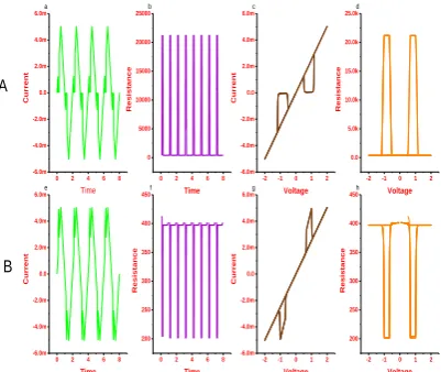
We examine the analysis by connecting two memristors in anti-parallel configuration as shown in figure 13. As we know the devices connected in opposite polarity have their switching characteristics in opposite manner, i.e. For applied voltage one
device is in ON state and another is in OFF state and vice versa, hence they form a spike like transitions for current and resistance and one device is almost in ON state, it plays major role in state change. In the first case as shown in figure 13(A), both devices are connected in anti-parallel and both are initially HRS, for positive voltage upto threshold, there is no state change occurs and both are in HRS, applied voltage is greater than threshold voltage the device which is forward biased change its state from OFF state to ON state and for negative voltage both change their states simultaneously. In the second case, forward biased device is in HRS and reversed device is LRS. This configuration is called anti parallel resistive switch (ARS) configuration. This is most important for designing logic gates and circuits like CRS concept. The V-I characteristics form truncated ohmic behavior, But it has the opposite characteristics to the CRS. After a complete cycle of input voltage the anti-parallel pair of memristors can work as ARS.
A single pair of anti-parallel memristors are necessary to form ARS. Now we will examine ten
pairs of anti-parallel memristor characteristics. In each ARS, the two memristors have equal thresholds, forward biased memristor is in HRS and reverse biased memristor is in LHS, the arrangement is as shown in figure 14. From the simulation results as shown in figure 15(A), We observe its functionality is same as single ARS and the current flowing through the circuit is five times of single ARS configurations because of the composite resistance is the parallel combination of five on resistances.
Figure 15. Characteristics of Multiple pairs of ARS circuits.
When one more forward biased and reverse biased memristor is added to multiple pairs of ARS circuits, it creates an additional memristance level As
0.00.51.01.52.0 -2.0m -1.5m -1.0m -500.0µ 0.0
0.00.5 1.0 1.5 2.0 0.0 20.0k 40.0k 60.0k 80.0k 100.0k 120.0k
-2 -1 0 1 2 -2.0m -1.5m -1.0m -500.0µ 0.0
-2 -1 0 1 2 0.0 20.0k 40.0k 60.0k 80.0k 100.0k 120.0k
0.00.51.01.52.0 -2.0m -1.5m -1.0m -500.0µ 0.0 500.0µ
0.00.5 1.0 1.5 2.0 0.0 20.0k 40.0k 60.0k 80.0k 100.0k 120.0k
-2 -1 0 1 2 -2.0m -1.5m -1.0m -500.0µ 0.0 500.0µ
-2 -1 0 1 2 0.0 20.0k 40.0k 60.0k 80.0k 100.0k 120.0k
0.00.51.01.52.0 -2.0m -1.5m -1.0m -500.0µ 0.0 500.0µ 1.0m
0.00.5 1.0 1.5 2.0 0.0 20.0k 40.0k 60.0k 80.0k 100.0k 120.0k
-2 -1 0 1 2 -2.0m -1.5m -1.0m -500.0µ 0.0 500.0µ 1.0m
-2 -1 0 1 2 0.0 20.0k 40.0k 60.0k 80.0k 100.0k 120.0k Cu r ren t Time a Res is tan ce Time b Cu r ren t Voltage c Res is tan ce Voltage d Cu r r en t Time e Res is tan ce Time f Cu r r en t Voltage g Res is tan ce Voltage h Cu r ren t Time i Res is tan ce Time j Cu r ren t Voltage k C B + -+ -ON ON + -+ -OFF ON + -+ -OFF OFF Res is tan ce Voltage l Initial state A
0 2 4 6 8
-6.0m -4.0m -2.0m 0.0 2.0m 4.0m 6.0m
0 2 4 6 8
0 1k 2k 3k 4k 5k 6k 7k 8k
-2 -1 0 1 2
-6.0m -4.0m -2.0m 0.0 2.0m 4.0m 6.0m
-2 -1 0 1 2
0 1k 2k 3k 4k 5k 6k 7k 8k
0 2 4 6 8
-4.0m -2.0m 0.0 2.0m 4.0m 6.0m
0 2 4 6 8
0 1k 2k 3k 4k 5k 6k 7k 8k 9k
-2 -1 0 1 2
-4.0m -2.0m 0.0 2.0m 4.0m 6.0m
-2 -1 0 1 2
0 1k 2k 3k 4k 5k 6k 7k 8k 9k
0 2 4 6 8
-6.0m -4.0m -2.0m 0.0 2.0m 4.0m
0 2 4 6 8
0 1k 2k 3k 4k 5k 6k 7k 8k 9k
-2 -1 0 1 2
-6.0m -4.0m -2.0m 0.0 2.0m 4.0m
-2 -1 0 1 2
Available online:
http://edupediapublications.org/journals/index.php/IJR/
P a g e | 3178shown in the figure 15(B) and 15(C) in the V-I characteristics and resistance characteristics. For a small voltage interval all the devices are in OFF state, before and after this interval it creates low and high memristance state. This configuration is useful for designing programmable logics in addition to logic LOW and HIGH, i.e. it creates three different memristance levels low, medium and high. From the simulation results of pair of ARS, its switching thresholds are small.
Figure 16. Characteristics of multi ARS circuits with asymmetry threshold voltages.
We examine the effect of the unequal threshold voltages on multiple (ten) pairs ARS circuit as shown in figure 16, we set the Vths and Vthr as 1V and -0.5v respectively. When |Vthr|< Vths then more current flows due to effective memristance ratio value is small as shown in figure 16(A). When |Vthr|> Vths then they create extensive low conduction intervals as shown in figure 16(B).
5.
Conclusion
In this paper we analyzed multiple interconnected memristors characteristics depends upon the orientation of device, circuit topology, current internal memristance and switching behavior by using SPICE tools. This analysis is very useful for implementing memristor logic gates and circuits by using the concept of CRS and ARS. Efficient parallel computing system can be designed by crossbar structure, memristor as a basic element in CRS.
6.
References
[1] Leon Chua, Resistive switching memories are memristors, Applied Physics, Vol.102 (2011), pp 765-783.
[2] Y. V. Pershin and M. Di Ventra, Memory effects in complex materials and nanoscale systems, advanced physics, Vol. 60(2011), 145-154.
[3] Y. V. Pershin and M. Di ventra, Practical approach to programmable analog circuits with memristors, IEEE transaction on circuits and systems, Vol. 57(2010), 1857-1864.
[4] M. Gholipour, N. Masoumi, Design investigation of nanoelectronic circuits using crossbar based nanoarchitectures, microelectronics journal, Vol. 44(2013), 190-200.
[5] K. H. Kim, S. Gaba, D. Wheeler, J. M. Cruz-albrecht, T. Hussain, N. Srinivasa and W. Lu, A functional hybrid memristor crossbar-array/CMOS system for data storage and neuromorphic applications, Nano letters, Vol. 12(2012), 389-395.
[6] U. Ruhrmair, C. Jaeger, M. Stutzmann, P. Lugli and G. Csaba. Applications of high capacity crossbar memories in crypography, IEEE transactions on Nanotechonology, Vol. 10(2011), 489-498.
[7] Y. V. pershin and M. Di Ventra, Solving mazes with memristors: a massively parallel approach, Physical Review, Vol 84(2011), 1-6.
[8] C. Yakopcic, T. M. Teha, and G. Subramanyam and R. E. Pino, Generalized Memristive device spice model and its application in circuit design, IEEE transaction on computer aidd design of integrated circuits and systems, Vol. 32(2013), 1201-1214.
[9] Wei-Hong Yin, Li-Dan Wang and Shu-Kai Duan, Characteristics of memristor series-parallel connection circuit with applications, Applied Mechanics and materials, Vol. 284-287(2013), 2485-2489.
[10] J. R. Heath, P. J. Kuekes, G. S. Snider, R. S. Williams, A defect tolerant computer architecture: opportunities for nanotechnology, Science, Vol. 280(1998), 1716-1721.
[11] M. D. Pickett, D. B. Strukov, J. L. Borghetti, J. J. Yang, G. S. Snider, D. R. Stewart and R. S. Wiliams, Switching dynamics in titanium dioxide memristive devices, Journal of applied physics, Vol. 106(2009), 392-297.
[12] J. Mustafa and R. Waser, A novel reference scheme for reading passive resistive crossbar memories, IEEE transaction on nanotechnology, Vol. 5(2006), 687-691.
[13] R. E. Pino, J. W. Bohl, N. McDonld, B. Wysocki, P. Rozwood, K. A. Campbell, A. Oblea and A. Timilsina, Compact method for modeling and simulation of memristor devices: ion conductor chalcognide based memristor devices, IEEE internatonal symposium on nanoscale architectures, Anaheim, CA, USA, 2010.
0 2 4 6 8
-6.0m -4.0m -2.0m 0.0 2.0m 4.0m 6.0m
0 2 4 6 8
0 5000 10000 15000 20000 25000
-2 -1 0 1 2
-6.0m -4.0m -2.0m 0.0 2.0m 4.0m 6.0m
-2 -1 0 1 2
0.0 5.0k 10.0k 15.0k 20.0k 25.0k
0 2 4 6 8
-6.0m -4.0m -2.0m 0.0 2.0m 4.0m 6.0m
0 2 4 6 8
200 250 300 350 400 450
-2 -1 0 1 2
-6.0m -4.0m -2.0m 0.0 2.0m 4.0m 6.0m
-2 -1 0 1 2
200 250 300 350 400 450
Current
Time
a
Resistanc
e
Time b
Current
Voltage c
Resistanc
e
Voltage d
Current
Time e
Resistanc
e
Time f
Current
Voltage g
Resistanc
e
Voltage h
A