ISSN (Print) : 2320 – 3765 ISSN (Online): 2278 – 8875
I
nternational
J
ournal of
A
dvanced
R
esearch in
E
lectrical,
E
lectronics and
I
nstrumentation
E
ngineering
(An ISO 3297: 2007 Certified Organization)
Vol. 4, Issue 4, April 2015
A New Methodology for Asynchronous
Systems
C S Manikandababu1, Lakshman K V2
Assistant Professor, Dept. of ECE, Sri Ramakrishna Engineering College, Coimbatore, Tamilnadu, India1 PG Student [VLSI], Dept. of ECE, Sri Ramakrishna Engineering College, Coimbatore, Tamilnadu, India2
ABSTRACT: As design systems have grown in complexity and clock speeds are constantly increasing, several limitations to the conceptual framework of synchronous design have begun to be noticed. Some notable problems due to higher performance demand are clock skew, power dissipation, interfacing difficulties and worst case performance. It is therefore not a surprise that the area of asynchronous circuits and systems, which generally do not suffer from these problems, is experiencing a significant resurgence of interest and research activity. Here we take into account new research concept which improves digital system implementations, which is basically asynchronous digital design. Asynchronous systems can be realized using clock-less chip implementation techniques which avoids the clock. This system gives importance to the arrival of data and sequence, only when required, thus reducing power consumption, EMI etc. The proposed methodology ensures the validity of the data by taking care of glitches, delays and hazards. The design of a new methodology for asynchronous system development and implementation of a simple ALU with the proposed methodology is discussed in this paper.
KEYWORDS: Asynchronous Design, Clock less system, Data completion, Null Convention Logic, Threshold gate.
I. INTRODUCTION
ITRS (International Technology Roadmap for Semiconductors) predicts likely shift from synchronous to asynchronous design styles, in order to increase circuit robustness, decrease power, and alleviate many clock-related issues. Furthermore, ITRS states that asynchronous circuits will account for 19% of chip area within the next 5 years, and 30% of chip area within the next 10 years. Functional improvement and performance balancing are crucial to successful microprocessor designs. According to Moore’s law, by 2017 CMOS clock frequency will be around 28.7 GHz. Rapid developments in VLSI technology caused smaller circuits and increased speed of communication.
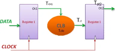
Traditional digital system designs in synchronous domain use pipelining and multithreading to increase throughput. Higher clock frequencies degrade the performance by way of clock-skew, glitches, meta-stability, hazards etc [3]. The clock-skew results in the violation of setup and hold time. Consider a Synchronous system, typically modelled by a register followed by a combinatorial logic as shown in Fig 1.
Fig 1.Block diagram of Synchronous pipeline system
ISSN (Print) : 2320 – 3765 ISSN (Online): 2278 – 8875
I
nternational
J
ournal of
A
dvanced
R
esearch in
E
lectrical,
E
lectronics and
I
nstrumentation
E
ngineering
(An ISO 3297: 2007 Certified Organization)
Vol. 4, Issue 4, April 2015
Minimum computation cycle time (Tc(min)) depends on the register delay time, combinatorial path delay, set up and hold time.
Tc(min)= Tot1 + Tlb + Tst+ Tot2 Tc(min) : Minimum cycle time
Tot1 : Clock to output delay of register 1 Tlb : Total worst case delay of the logic block Tst : Setup time of register 2
Tot2 : Clock to output delay of register.
Consider Fig 2. Assume that each clock edge arrives at each register at a precise time (tp). The main sources of delays in the clock distribution networks are RC wire delays, LC ringing on the clock nets and buffer delays.
Fig. 2 Skew problems in synchronous domain
Register-1, which is clocked at Tcl1, passes the data to the logic block and after the completion of operation the data is passed to register-2. At that time register-2 passes the previous data to the output terminal. But the wire delays in the clock line results in the latching of incorrect data at register 2. In synchronous system computation time depends on the critical path. Consider three combinatorial blocks with delays in the order of 10s, 20s and 30s, so in the synchronous domain that will work only in 30s delay, which means that Synchronous design styles are in worse case delay type [1][2].
Clock signal is generated by oscillator. Higher rate of clock increases the power consumption and causes EMI. Clock tree distribution overcomes problems in synchronous circuit such as skew and glitches that are present in the global distribution of clock signal. The complex oscillator circuitry, the clock distribution tree and multithreading technique can occupy large logic area and power consumption [3].So we go with clock less/asynchronous systems where all these problems are eliminated.
II. ASYNCHRONOUS SYSTEMS
In the asynchronous design style, logical blocks are not waiting for global clock events; the next block starts the operation when the previous block completes its operation [3]. General rule used in the asynchronous system is that data transfer occurs when the next block returns to idle state and the previous block completes an operation and produces a new value to the input of the succeeding block. This is the basic idea of asynchronous systems [4][5].Asynchronous circuits fall into two main categories: delay-insensitive(DI) and bounded-delay models [4]. DI uses handshaking protocols to achieve control over the circuit. A request signal is sent to previous functional modules requesting a new data after finishing its current operation. The previous block transfer the new data after receiving the request signal if it has completed its current operation. Otherwise the data is held. The delay insensitive circuits are insensitive to propagation delay of gates and wires. Paradigms, like Null Convention Logic(NCL) circuits, assume delays in both logic elements and interconnect to be unbounded, although they assume that wire forks are isochronic [5][6]. This means that wire delays within a component are much fewer than the logic element delays in the component, and this assumption is also valid in nanometer scale technologies. Wires connecting components do not need to adhere to the isochronic fork assumption. NCL circuits often outperform other delay-insensitive methods because they target a wider range of logical operators.
ISSN (Print) : 2320 – 3765 ISSN (Online): 2278 – 8875
I
nternational
J
ournal of
A
dvanced
R
esearch in
E
lectrical,
E
lectronics and
I
nstrumentation
E
ngineering
(An ISO 3297: 2007 Certified Organization)
Vol. 4, Issue 4, April 2015
Fig.3 Delay Insensitive Asynchronous system
Bounded delay model consist of delay lines. The propagation delay of the delay lines should be greater than the propagation delay of the functional block. The Bounded Delay asynchronous logic is shown in the Fig 4.
Fig.4 Bounded Delay Asynchronous system
A. Null Convention Logic(NCL)
NCL provides an asynchronous design methodology by incorporating data and control information into one mixed path such that there is no need for worst-case delay analysis and control path delay matching [1]. NCL relies on symbolic completeness of expression to achieve self-timed behavior. Traditional Boolean logic is not symbolically complete because the output of a Boolean gate is only valid when referenced with time. NCL eliminates this time-reference problem by employing dual-rail or quad-rail signals. A dual-rail signal, D, consists of two mutually exclusive wires, D0 and D1, which may assume any value from the set {DATA0, DATA1, NULL},as shown in Table 1
Table 1. Dual rail Encoding
All NCL systems must satisfy the following two criteria to be delay-insensitive. Input Completeness and Observability.The conditions for Input completeness are :
(i) The outputs of a circuit may not transition from NULL to DATA until all inputs havetransitioned from NULL to DATA.
(ii) The outputs of a circuit may not transition from DATA to NULL until all inputs have transitioned from DATA to NULL.
According to Seitz's "weak conditions" of delay-insensitive signalling, an output can transition without a complete input set as long as all outputs cannot transition before all inputs arrive [14].For Observability, Every gate transition must be observable at one or more circuit outputs, which means that any gate that transitions will cause at least one output to transition. NCL uses threshold gates with hysteresis for its composable logic elements. Such an operator consists of a set condition and a reset condition that the environment must ensure are not both satisfied at the same
WAVEFRONT True Value False Value
DATA 1 1 0
DATA 0 0 1
NULL 0 0
ISSN (Print) : 2320 – 3765 ISSN (Online): 2278 – 8875
I
nternational
J
ournal of
A
dvanced
R
esearch in
E
lectrical,
E
lectronics and
I
nstrumentation
E
ngineering
(An ISO 3297: 2007 Certified Organization)
Vol. 4, Issue 4, April 2015
time. If neither condition is satisfied, then the operator maintains its current state. One type of threshold gate is the THmn gate, where 1 ≤ m ≤ n, as depicted in Fig5. THmn gates have n inputs. At least m of the n inputs must be asserted
before the output will be asserted, which is the gate’s set condition. Because NCL threshold gates are designed with hysteresis, all asserted inputs must be deasserted before the output will be de-asserted, which is the reset condition [5]. Thus, any threshold gate can be represented in terms of its set and reset condition: Z = f + (g • Z*), where f is the set condition, g is the complement of the reset condition, and Z* is the previous value of the output Z. Most threshold gates employ gate internal feedback paths in order to satisfy the hysteresis condition, represented by (g • Z*) in the above equation.As an example, consider the TH23 gate whose output Z is asserted when at least two of its three inputs (i.e., A, B, C) are asserted, remaining asserted until all inputs are deasserted.The TH23 gate is represented by Z = AB + BC + AC + ((A + B + C) • Z*) and is depicted in Fig 6.
Fig.5 Threshold gate
Fig.6 RTL of TH23 gate
Fig.7 NCL System Implementation
ISSN (Print) : 2320 – 3765 ISSN (Online): 2278 – 8875
I
nternational
J
ournal of
A
dvanced
R
esearch in
E
lectrical,
E
lectronics and
I
nstrumentation
E
ngineering
(An ISO 3297: 2007 Certified Organization)
Vol. 4, Issue 4, April 2015
acknowledgement mechanism of register interaction ensures a two phase discipline in NCL system functioning and prevents collisions between different Data wave fronts. As seen in Fig 7, NCL system consists of three components: combinational logic, registers, and completion logic, all consisting of threshold gates.
Some of the previous methods were delay insensitive minterm synthesis (DIMS), Seitz’s and Anantharaman’s approaches require the generation of all minterms, no optimization is possible[5]. However, Singh’s and David’s approaches[6] allow for some Boolean optimization to be performed, but they may not facilitate the same potential for optimization provided by NCL’s many state-holding gates. This paper proposes a new methodology for asynchronous digital system design, which overcome all the drawbacks of existing asynchronous digital system.
III.PROPOSED METHODOLOGY
The proposed methodology for Asynchronous System Design is shown in the Fig 8. This methodology starts from Synchronous HDL code to end up with Asynchronous Layout. Technology mapping was done to a custom library. The Single rail to Dual rail conversion was performed as soon as the synchronous HDL netlist was generated. Asynchronous netlist was created in terms of TOOL specific components. Initially, all these components were mapped to generic library to check the functionality and then to a custom library. Thus asynchronous netlist in terms of library components was made. By using P&R tool, asynchronous layout was obtained. To prove this methodology, we considered a simple two bit Arithmetic and Logic Unit(ALU),which perform two operations addition and subtraction. User can make selection on type of operation to be performed.
Fig.8 Proposed Methodology
Once the synchronous code for ALU was provided, synthesis was done. The structural view of synchronous HDL netlist is shown below. It is the single rail netlist. It consists of d-flip-flop, two input and gate, xor gates& multiplexer and an inverter. In addition to that, it has a global clock, meaning to say that, at present the system is synchronous.
Synchronous HDL code
Synchronous HDL Netlist
Asynchronous HDL Netlist in terms of TOOL specific components
Asynchronous Layout
Synthesis
Single rail to Dual Rail Conversion
Technology Mapping
Floor Planning, Place and Route
Asynchronous HDL Netlist in terms of generic components
Generic library
Custom library
Mapping to generic library
ISSN (Print) : 2320 – 3765 ISSN (Online): 2278 – 8875
I
nternational
J
ournal of
A
dvanced
R
esearch in
E
lectrical,
E
lectronics and
I
nstrumentation
E
ngineering
(An ISO 3297: 2007 Certified Organization)
Vol. 4, Issue 4, April 2015
Fig.9 Structural view of Single rail Netlist
In order to make the system asynchronous, we need to remove the clock. So, making the system dual rail and mapping to threshold gates, the system becomes asynchronous.Fig.10 shows structural representation of the asynchronous netlist.TH22 ,TH33w2, TH24comp etc are the NCL threshold gates, drlatr&drlatn are the latches which allows the
system to satisfy the NCL conditions.
Fig.10 Structural view of Asynchronous Netlist
IV.RESULTS
A simple two bit ALU which perform two operations was our design to prove proposed methodology. In order to verify the functional correctness, both synchronous and asynchronous two bit ALUs were simulated and they
clk dff d ck dff d R[1] ck R[0] xor2 a y b B[0] A[0] xor2 a y b xor2 a y b Op B[1] A[1] N7
N8 q q
ISSN (Print) : 2320 – 3765 ISSN (Online): 2278 – 8875
I
nternational
J
ournal of
A
dvanced
R
esearch in
E
lectrical,
E
lectronics and
I
nstrumentation
E
ngineering
(An ISO 3297: 2007 Certified Organization)
Vol. 4, Issue 4, April 2015
showed same result. The simulation results of synchronous and asynchronous designs are depicted in Fig 11&12 respectively.
Fig.11 Simulation result for Synchronous ALU
Fig.12 Simulation result for Asynchronous ALU
After simulation, physical design has to be performed according to methodology. By using existing CAD tools, it is difficult to perform P&R .But fortunately, for NCL circuits, we can perform place and route using existing CAD tools [8].That was another reason for opting NCL circuits. Fig 13 shows the asynchronous layout for two bit ALU.
ISSN (Print) : 2320 – 3765 ISSN (Online): 2278 – 8875
I
nternational
J
ournal of
A
dvanced
R
esearch in
E
lectrical,
E
lectronics and
I
nstrumentation
E
ngineering
(An ISO 3297: 2007 Certified Organization)
Vol. 4, Issue 4, April 2015
V.CHALLENGES
The asynchronous system development is very difficult and complex due to hazard elimination and synchronization. Proper hazard elimination causes large area overhead. In asynchronous design, complex timing analysis makes it difficult to estimate the performance. The system cannot be tested easily. Lack of CAD tools, immature synthesis methodologies and the lack of designer expertise are reasons for asynchronous systems not to be widely used.
VI.CONCLUSION
Asynchronous digital systems are advantageous over synchronous digital systems. EMI, skew and power consumption are reduced in asynchronous systems. But they generally suffer from hazards, data validity issues, high power consumption by the internal sub systems and design complexity. The proposed asynchronous system overcomes all these problems.
REFERENCES
[1]Davis. A, Nowick.S.M“An Introduction to Asynchronous Circuit Design”, 1997
[2] Ad Peeters“Hand shake solution” Asynchronous silicon compilation symposium 20 Years OOTI, March 26, 2009. [3] Adam Megacz, “Clock less Circuits, Berkeley”, EECS, CS150,2009.
[4]Karl M fant, Scott a Brandt “Theseus logic Null convention logic”, Theseus logic.inc 1997.
[5] T.S. Anantharaman, A delay insensitive regular expression recognizer, IEEE VLSI Techn. Bull. September (1986).
[6] N.P. Singh, A design methodology for self-timed systems, Master’s Thesis, MIT/LCS/TR-258, Laboratory for Computer Science, MIT, 1981. [7] Scott C Smith & Jai di,“ Designing asynchronous circuit using Null Convention logic”,synthesis lectures on digital circuits’& systems,Mitchell
a Thornton, servo editor, Morgan & clay pool publishers.