Implementation
of
Parallel-Prefix
Adders using Reverse
Converter
*K.SNEHA **MR.G.BABU **MR.T.SAMMAIAH
*M.TECH Dept of ECE,VAAGDEVI COLLEGE OF ENGINEERING
**Assoc. prof Dept of ECE, VAAGDEVI COLLEGE OF ENGINEERING
***Assoc. prof Dept of ECE, VAAGDEVI COLLEGE OF ENGINEERING
Abstract:
In this project, the implementation of
residue number system reverse converters
based on well-known regular and modular
parallel prefix adders is analyzed. The VLSI
implementation results show a significant
delay reduction and area × time2
improvements, all this at the cost of higher
power consumption, which is the main
reason preventing the use of parallel-prefix
adders to achieve high-speed reverse
converters in nowadays systems. Hence, to
solve the high power consumption problem,
novel specific hybrid parallel-prefix-based
adder components that provide better
tradeoff between delay and power
consumption are here in presented to design
reverse converters. A methodology is also
described to design reverse converters based
on different kinds of prefix adders. This
methodology helps the designer to adjust the
performance of the reverse converter based
on the target application and existing
constraints.
I. INTRODUCTION
The Residue Number System plays a
significant role in the battery based and
portable devices because of its low power
features and its competitive delay. The
Residue number system reverse converter is
using new components methodology for
higher speed operation[1].The RNS consists
of two main components forward and the
reverse converter that are integrated with the
existing digital system. The forward
converter performs the operation of
converting the binary number to the modulo
number whereas the reverse converter
performs the operation of reverse converting
the modulo number to the binary number
which is the hard and time consuming
process compared with the forward
converter. The fundamental RNS concepts
such as 1)RNS definition with properties
and their applications,2)consideration of
modulo set selection,3)design of forward
converter,4)modulo arithmetic
units,4)design of reverse converter are
discussed[2]. The voltage over scaling
(VOS) technique is applied to the residue
number system to achieve high energy
efficiency.
The VOS technique introduces soft errors
which degrades the performance of the
system. To overcome these soft errors a new
technique is implemented called joint
RNS-RPR (JRR) which is the combination of
RNS and the reduced precision redundancy.
This method provides the advantage of
satisfying the basic properties of RNS
includes shorter critical path, reduced
complexity and low power[3].New
architectures are presented for the moduli
sets(2n-1,2n,2n+1) for the conversion from
the residue to the binary equivalents[4].Here
the speed and the cost are major concern.
Distributed arithmetic principles are used to
perform the inner product computation
in[5].The input data which are in the residue
domain which are encoded using the
Thermometer code format and the outputs
are encoded using the One hot code format.
Compared to the conventional method
which used Binary code format, the
proposed system which achieves higher
operating speed.
The residue number system which provides
carry free addition and fully arithmetic
operation [6], for several applications such
as digital signal processing and
cryptography[7]-[11]. In this brief, we
present a comprehensive method which uses
the parallel prefix adder in selected position,
thereby using the shift operation on one bit
module to achieve a fast reverse converter
design. The usage on parallel prefix
structure in the design leads to higher speed
in operation meanwhile it increases the area
and power consumption. In order to
compensate the tradeoff between the speed,
area and power consumption, a novel
specific hybrid parallel prefix based adder
components are used to design the reverse
converter. These hybrid design which
provides the significant reduction in the
power delay product (PDP)metric and leads
to considerable improvements in the area x
time² product(AT²) in comparison with the
traditional converters without using parallel
prefix adders.
II.
PARALLEL PREFIX STRUCTURE
The Residue number system mainly
composed of three main parts such as,
forward converter, modulo arithmeticunits
and reverse converter. On comparing with
the other parts the reverse converter design
is a complex and non modular structure. So
more attention is needed in designing the
reverse converter thereby preventing the
slow operation and compromise the benefits
of the RNS. The parallel prefix structure
helps to achieve the faster operation in the
reverse converter design but causes
increased power consumption. In the
existing system the novel specific hybrid
parallel prefix adder based components are
used to replace the existing components
thereby reducing the power consumption
and getting faster operation.
The Parallel prefix structure consists of three
main blocks, they are preprocessing block,
prefix carry tree and post processing block.
The parallel prefix adder operation begins
with preprocessing stage by generating the
Generate (Gi) and Propogate (Pi) equation
[1] & [3]. The prefix carry tree get
proceeded with the previous block signal to
yield all carry bit signal and these stage
contains three logic complex cells such as
cell compute both the propogate (P(i,j)) and
generate (G(i,j)) by using the equation[3]
&[4].The Gray cell executes only the
generate(G(i,j)).The carry bits generated in
the second stage get passed to the post
processing block thereby generating the sum
using the equation[5].The block diagram is
shown in the
Fig.1
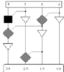
The Brent Kung adder prefix structure is
employed to achieve the higher speed with
reduced power consumption. On comparing
with the other parallel prefix adder structure
the BK adder is chosen mainly for minimum
fan out and should be higher speed in
operation than others.Fig.2 shows the
example BK adder prefix structure which
uses the three basic cells in the prefix
structure. These structure is elaborated for
the proposed design having the modulo
addition of (4n+1) for n=5.
B. HRPX Structure: (Hybrid Regular Parallel Prefix XOR/OR Adder Component)
Fig. 4 shows HRPX Structure. The regular
parallel prefix adder is used to do the first
part of addition and the simplified RCA
logic is used to do the second part where the
corresponding bits of the operand are fully
variable. Full adder can be designed with
XOR/OR gates because of the constant
operand. In these reverse converter design
the carry chain is not needed and can be
ignored. For most modulo sets (2ⁿ-1)
addition is an necessary operation. The End
represented with two zero, but for the
reverse converter design one zero
representation is required. To correct these
zero representation problem, a detector
circuit was employed in the design but it
incorporates additional delay. So, the Binary
to excess one converter(BEC) is used to
solve the double zero representation issue.
C. HMPE Structure (Hybrid Modular Parallel Prefix Excess One Adder Component)
The HMPE Structure consists of two parts:
Regular prefix adder and the Modified
Excess One unit as shown in Fig.3. The first
two operands are added using the parallel
prefix adder and the result is conditionally
incremented based on the control signal
generated by the prefix structure to assure
the single zero representation.
III. PROPOSED METHODOLOGY A. Introduction
The RNS (Residue Number System) can
provide carry free and fully parallel
arithmetic operations for several
applications, including digital signal
processing and cryptography. In this brief,
for the first time, we present a
comprehensive methodology to wisely
employ parallel-prefix adders in carefully
selected positions in order to design fast
reverse converters. The usage of the
parallel-prefix adders to implement
converters highly increases the speed at the
expense of additional area and remarkable
increase of power consumption. The reverse
converter consists of a complex and
non-modular structure. Therefore, more attention
should be directed to its design to prevent
slow operation and compromise the benefits
of the RNS. Both the characteristics of the
moduli set and conversion algorithm have
significanteffects on the reverse converter
performance. In addition to the moduli set,
hardware components selection is key to the
RNS performance.
Prefix: The outcome of the operation depends upon the initial inputs.
Parallel: involves the execution of an operation in parallel. This is done by
segmentation into smaller pieces that are
computed in parallel.
Operation: any arbitrary operator that is associative is parallelizable.
It is very fast because the processing is
the use of modular and regular
parallel-prefix adders proposed in this brief in
reverse converters highly decrease the delay
at the expense of significantly more power
and circuit area, whereas the proposed
prefix-based adder components allows one
to achieve suitable tradeoffs between speed
and cost by choosing the right adders for the
parts of the circuits that can benefit from
The basic cells used for the parallel prefix
operations in these projects are as shown in
the above fig.5. If high speed is the designer
goal, the CPAs with EAC and the regular
CPAs should be replaced by traditional
parallel prefix modulo 2n – 1 adder and
regular parallel-prefix adders, respectively.
However, for the VLSI designers, a suitable
tradeoff between speed, power, and area is
often more important. a regular
parallel-prefix adder with the desirable parallel-prefix
structure can be used to perform the first
part of the addition, for which the
corresponding bits of the operands are fully
variable, and a RCA with simplified logic to
do the second part (full adder becomes
XNOR/OR gates because of the constant
operand). The proposed hybrid regular
parallel-prefix XOR/OR (HRPX) adder
component to perform the (4n + 1)-bit
addition. It should be noticed that due to the
architecture of the reverse converter, the
carry output of the XNOR/OR chain is not
needed and can be ignored as shown in
Fig.6.
The regular CPA with end around carry is
by default a moduli 2n − 1 adder with
double representation of zero, but in reverse
converters a single representation of zero is
required. So, a one detector circuit has to be
used to correct the result, which imposes an
additional delay. However, there is a
modified to fix the double-representation of
zero issue.
B. Kogge Stone Prefix Adder
KSA is a parallel prefix form Ripple carry
adder. It generates carry in O (logn) time
and is widely considered as the fastest adder
and is widely used in the industry for high
performance arithmetic circuits as shown in
Fig.7. In KSA, carries are computed fast by
computing them in parallel at the cost of
increased area. The complete functioning of
KSA can be easily comprehended by
analyzing it in terms of three distinct parts:
1. Pre Processing: This step involves computation of generate and
propagate signals corresponding too
each pair of bits in A and B. These
signals are given by the logic
equations below:
2. Ripple Carry Adder Network: This block differentiates KSA from other
adders and is the main force behind
its high performance. This step
involves computation of carries
corresponding to each bit. It uses
group propagate and generate as
intermediate signals which are given
by the logic equations below:
3. Post Processing: This is the final step and is common to all adders of
this family (carry look ahead). It
involves computation of sum bits.
Sum bits are computed by the logic
given below:
4. Implementation: The schematic of KSA is implemented by using
following building blocks:
Bit Propagate and Generate: This block implements the following
logic:
Group Propagate and Generate:
This block implements the following
Group Propagate and Generate:
This block implements the following
logic:
IV. SIMULATION RESULTS
In this chapter all the simulation results which are done using Xilinx ISE 9.1 are shown in
below results.
V. CONCLUSION This project presents a method that can be applied to most of the
current reverse converter architectures to
enhance their performance and adjust the
cost/performance to the application
specifications. The use of modular and
regular parallel-prefix adders proposed in
this brief in reverse converters highly
decrease the delay at the expense of
significantly more power and circuit area,
whereas the proposed prefix-based adder
components allows one to achieve suitable
tradeoffs between speed and cost by
choosing the right adders for the parts of the
circuits that can benefit from them the most.
Performance increased by using kogge stone
adder implementation.
VI. REFERENCES [1] Azadeh Alsadat Emrani Zarandi, Amir Sabbagh
Molahosseini, Mehdi Hosseinzadeh, Saeid
Sorouri, Samuel Antão, and Leonel Sousa ,
Reverse Converter Design via
Parallel-Prefix Adders: Novel Components,
Methodology, and Implementations‖ in
IEEE Trans. on VLSI SYSTEMS., January
16, 2014
[2] K. Navi, A. S. Molahosseini, and M.
Esmaeildoust, How to teach residue number
system to computer scientists and engineers,
IEEE Trans. Educ., vol. 54, no. 1, pp. 156–
163, Feb. 2011.
[3] J. Chen and J. Hu, Energy-efficient
digital signal processing via voltageover
scaling-based residue number system, IEEE
Trans. Very Large Scale Integr. (VLSI)
Syst., vol. 21, no. 7, pp.
1322–1332, Jul. 2013.
[4] A. Benjamin Premkumar, M. Bhardwaj,
and T. Srikanthan , High-Speed and
Low-Cost Reverse Converters for the
(2n-1,2n,2n+1) Moduli Set, IEEE Trans. on
circuits and systemsII: Analog and Digital
Signal Processing, vol. 45, no. 7, July 1998.
[5] Chan Hua Vun, Senior Member, IEEE,
Annamalai Benjamin Premkumar, Senior
Member, IEEE, and Wei Zhang, Member,
IEEE, A New RNS based DA Approach for
Inner Product Computational, IEEE
Trans.Circuits and Systems I: Regular
Papers, vol. 60, no. 8, AugusT 2013.
[6] A. Omondi and B. Premkumar, Residue
Number Systems: Theory and
Implementations. London, U.K.: Imperial
[7] B. Parhami, Computer Arithmetic:
Algorithms and Hardware Designs,2nd ed.,
New York, NY, USA: Oxford Univ. Press,
2010.
AUTHOR 1:-
*K.SNEHA completed her
B.Tech in JAYAMUKHI INSTITUTE OF
TECHNOLOGY SCIENCES in 2014 and
M.Tech completed in VAAGDEVI
COLLEGE OF ENGINEERING
AUTHOR 2:-
** Mr.G.BABU working as
Assoc. prof in Dept of ECE, VAAGDEVI
COLLEGE OF ENGINEERING
AUTHOR3:-
***Mr.T.SAMMAIAH working
as Assoc. prof in Dept of ECE, VAAGDEVI
COLLEGE OF ENGINEERING