DESIGNS AND ANALYSES OF SOME RF/MICROWAVE PASSIVE ELEMENTS ON CYLINDRICAL CPWS
V. Akan
Communication System Group
TUBITAK Space Technologies Research Institute ODTU Kampusu
Inonu Bulvari, TR-06531, Ankara, Turkiye
M. Duyar
Republic of Turkiye Ministry of Industry and Trade Ankara, Turkiye
E. Yazgan
Department of Electrical and Electronics Engineering Hacettepe University
TR-06800, Ankara Turkiye
M. Bayrak
Faculty of Engineering
Department of Electrical and Electronics Engineering Selcuk University
Konya, Turkiye
Abstract—In this article, designs and analyses of several CCPW (Cylindrical CPW) discontinuities have been realized as microwave
reactive elements. The quasi-TEM characteristic parameters
of CCPWs have been obtained by CMT (Conformal Mapping Techniques) which provide satisfactory accuracy at microwave frequencies and lead to closed-form analytical solutions suitable
for CAD software packages. Then these discontinuities have been
simulated in CST Microwave Studio 2006 in order to obtain inductance, capacitance and also input impedance versus frequency and physical dimensions of the elements. The results show that CCPW
discontinuities can be used successfully as reactive elements for related applications.
1. INTRODUCTION
There is a growing interest in non-planar transmission lines recently. Since these type transmission lines are quite flexible they can be especially applied in aircraft, missiles, and mobile communication applications in order to feed printed antennas around a non-planar surface like an elliptical or a cylindrical surface where the planar
realization is not feasible as mentioned in [1, 2]. It is possible
to construct cylindrical and/or elliptical transmission lines using
appropriate dielectric materials easily. Up to date there are some
studies about non-planar transmission lines to evaluate characteristic
parameters of them analytically and accurately [1–5]. In addition,
various planar and cylindrical CPW discontinuities have been analyzed in [6–8]. In these papers, mostly, similar capacitive elements have been taken into consideration for cylindrical applications. However, in this study it is aimed to analyze and design of CCPW short circuit inductive, CCPW open ended-capacitive and CCPW open circuit with gap-capacitive elements. In order to calculate the characteristic parameters of CCPWs CMT has been employed. These parameters are also verified by simulations in CST Microwave Studio 2006. Moreover, input impedance and inductance or capacitance values have
been obtained according to defined line parameters. The realized
calculations and simulations indicate that studied elements can be used easily in the related applications.
2. CALCULATION OF CHARACTERISTIC LINE PARAMETERS FOR CCPW
In Fig. 1, cross sectional view of the transmission line used to form CCPW discontinuities is seen with defined physical parameters. The characteristic impedance and effective dielectric constant of CCPW can be calculated as follows [3, 4, 9]
CT =C01+C03+Cd (1)
whereC0 andCdcapacitances stand for the free-space capacitance per unit length and the dielectric layer respectively. CT also refers to total capacitance per unit length. Air capacitance can be expressed as:
C01=C03= 2ε0K
(k0)
whereK(k) is the complete elliptic integral of the first kind. Similarly, the capacitance of the dielectric layer is,
Figure 1. The cross-sectional view of CCPW for the construction of the related discontinuities.
Cd= 2ε0(εr−1)K (kd)
K(kd) (3)
Then effective dielectric constant and characteristic impedance of CCPW can be written as
εeff = CT C0
= 1 +q(εr−1) (4)
whereq is the filling factor that can be expressed as
q= 1
2
K(kd)K(k0) K(kd)K(k0)
(5)
and finally the characteristic impedance relation can be obtained as
Z0 =
30π √ε
eff
K(k0) K(k0)
(6)
Reference plane
l
θ - Ψ
2Ψ
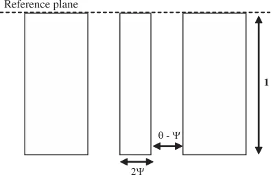
Figure 2. Planar visualization of CCPW short circuit inductive element where l= 1.65 mm.
4.15 4.1
4.05
4
3.95
3.9
3.85
3.8
0.5 1.5 2.5 3.5 4.5 5.5 6.5 7.5 8.5 9.5
Inductance (Henry)
Frequency (GHz)
(a)
30
25
20
15
10
5
0
0.5 1.5 2.5 3.5 4.5 5.5 6.5 7.5 8.5 9.5
Frequency (GHz)
(b)
5
4
3
2
1
0
0.5 1.5 2.5 3.5 4.5 5.5 6.5 7.5 8.5 9.5
Frequency (GHz)
(c)
Real Part of Zin
Imaginary Part of Zin
x 10-10
x 10-3
3. CCPW DISCONTINUITIES
According to Fig. 1, 2Ψ and 2θ refer to central conductor width and total width of central conductor and gaps, respectively. r1, r2 are
inner and outer radius of dielectric material, respectively as well. All conductors are assumed as PEC and having zero thickness. Dielectric materials are also supposed as simple mediums. Through the analyses and designs all of the studied elements have been realized on 50 ohm CCPW, in this paper i.e., 2Ψ = 60◦, 2θ = 115.94◦, r1 = 2.4 mm,
r2 = 6.2 mm andεr= 2.1.
3.1. CCPW Short Circuit Element
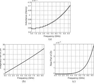
In Fig. 2, the planar visualization of CCPW short circuit inductive
element is shown with defined dimensions. In this case, when the
element is excited current flows around joint of ground and signal conductors, then magnetic energy is stored behind this joint and this response increases the reactance inductively. In Fig. 3, real and imaginary parts of input impedance and inductance values are seen in 0.5–10 GHz frequency range for the given parameters.
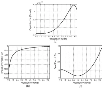
3.2. CCPW Open Ended Element
This element again has the same cross sectional dimensions as seen in Fig. 1. Its planar illustration is also seen in Fig. 4. Similar to the short circuit element, because of abrupt change at the end, fringing fields arise and they give rise to stored electric energy. This case leads to increase in capacitive reactance. The obtained results for real and
Reference plane
1
θ - Ψ
2Ψ
4.5
4
3.5
3
2.5 x 10⁻¹³
0.5 1.5 2.5 3.5 4.5 5.5 6.5 7.5 8.5 9.5
Frequency (GHz)
(a)
Capacitance (Farad)
0
-200
-400
-600
-800
-1000
-1200
-1400
0.5 1.5 2.5 3.5 4.5 5.5 6.5 7.5 8.5 9.5
Frequency (GHz)
(b)
40
30
20
10
0
0.5 1.5 2.5 3.5 4.5 5.5 6.5 7.5 8.5 9.5
Frequency (GHz)
(c)
Real Part of Zin
Imaginary Part of Zin
Figure 5. (a) Capacitance, (b) imaginary, and (c) real part of input impedance values of the CCPW open ended capacitive element.
Reference plane
l g
θ - Ψ
2Ψ
imaginary parts of input impedance and total capacitance value of this element are shown in Fig. 5 according to the defined parameters.
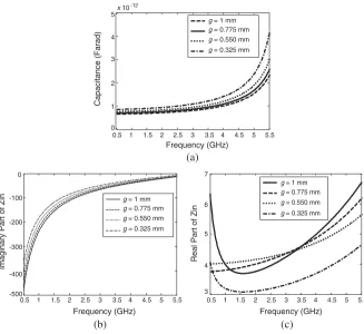
3.3. CCPW Open Circuit with a Gap
The last element is again a capacitive one. For cross sectional view Fig. 1 can be referenced and in Fig. 6 planar visualization of CCPW open circuit with a gap is seen with the related dimensions. For this element, because of the gap placed in the center conductor, there exists electric field that increases capacitive reactance. Simulation results for input impedance and total capacitance are shown in Fig. 7 for the related dimensions, and effect of gap length is clearly seen on capacitive reactance value. " " 5 4 3 2 1 0
0.5 1 1.5 2 2.5 3 3.5 4 4.5 5 5.5
Capacitance (Farad)
Frequency (GHz)
g = 0.775 mm g = 0.550 mm g = 0.325 mm g = 1 mm
(a) 0 -100 -200 -300 -400 -500
Imaginary Part of Zin
g = 0.775 mm g = 0.550 mm g = 0.325 mm g = 1 mm
0.5 1 1.5 2 2.5 3 3.5 4 4.5 5 5.5
Frequency (GHz)
(b)
0.5 1 1.5 2 2.5 3 3.5 4 4.5 5 5.5
Frequency (GHz) (c) 7 6 5 4 3
Real Part of Zin
g = 0.775 mm g = 0.550 mm
g = 0.325 mm g = 1 mm x 10-12
4. CONCLUSION
In this paper, CCPW short circuit element, CCPW open ended element and CCPW open circuit with a gap have been designed and simulated. First of all, the characteristic impedance and effective dielectric constant have been evaluated via CMT. Then using appropriate dimensions, the mentioned elements have been designed and simulated
in CST Microwave Studio 2006. In addition, input impedance as
real and imaginary parts, inductance and total capacitance have been presented for the simulated elements. The change of these obtained values versus freauency is similar to the results of planar cases. Briefly, in this article it is shown that RF/microwave reactive elements can be realized on CCPW type transmission lines. For the time being the experimental studies on these elements are going on, and as a future work they can be used for matching and feeding cylindrical wrap around type antennas.
ACKNOWLEDGMENT
This study has been supported by TUBITAK (The Scientific and Technological Research Council of Turkey) under grant EEEAG-105E022.
REFERENCES
1. Dib, N. and A. Omar, “Dispersion analysis of multilayer cylin-drical tranmission lines containing magnetized ferrite substrates,”
IEEE Trans. Microwave Tech., Vol. 50, No. 7, 1730–1736, July
2002.
2. Duyar, M., V. Akan, E. Yazgan, and M. Bayrak, “Analyses of elliptical coplanar coupled waveguides and coplanar coupled
waveguides with finite ground width,” IEEE Trans. Microwave
Tech., Vol. 54, No. 4, 1388–1395, June 2006.
3. Akan, V. and E. Yazgan, “Quasistatic TEM characteristics of multilayer elliptical and cylindrical coplanar waveguides,”
Microwave Opt. Tech. Lett., Vol. 42, No. 4, 317–322, Aug. 2004.
4. Yazgan, E. and V. Akan, “Conformal mapping techniques,”
Encyclopedia of RF and Microwave Engineering, Vol. 1, John
Wiley & Sons, 2005.
5. Karpuz, C., M. Duyar, and A. G¨or¨ur, “Analysis of
cylindrical conductor-backed coplanar waveguides,” Microwave
6. Al-Zoubi, A. and N. Dib, “CAD model of gap in cylindrical coplanar waveguide,” Electronics Letters, Vol. 35, No. 25, 1857– 1858, Oct. 1999.
7. Beilenhoff, K., H. Klingbeil, W. Heinrich, and H. L. Hartnagel,
“Open and short circuits in coplanar MMIC’s,”IEEE Trans.
Mi-crowave Tech., Vol. 41, No. 9, 1534–1537, Sep. 1993.
8. Simons, R. N. and G. E. Ponchak, “Modeling of some
coplanar waveguide discontinuities,” IEEE Trans. Microwave
Tech., Vol. 36, No. 12, Dec. 1998.
9. Su, H.-C. and K.-L. Wong, “Quasistatic solutions of cylindrical
coplanar waveguides,” Microwave and Optical Technology Lett.,