Architectural design proposal for real time clock for wireless
microcontroller unit
Muhammad Nor Azwan Mohd Alias1, *, and Shaiful Nizam Mohyar1 1School of Microelectronic Engineering, University Malaysia Perlis, 02600 Malaysia
Abstract. In this project, we are developing an Intellectual properties (IP) which is a dedicated real-time clock (RTC) system for a wireless microcontroller. This IP is developed using Verilog Hardware Description Language (Verilog HDL) and being simulated using Quartus II and Synopsys software. This RTC will be used in microcontroller system to provide precise time and date which can be used for various applications. It plays a very important role in the real-time systems like digital clock, attendance system, digital camera and more.
1 Introduction
A real-time clock (RTC) is a clock system that provide real time value used with system that deals with time. For example, it is included in a computer motherboard. It is an electronic device in the form of an Integrated Chip (IC) available in various packaging options. Memory on the RTC stores system description or setup values including current time values stored by the real-time clock. The time values are for the year, month, date, hours, minutes, and seconds. When the computer is turned on, the Basic Input-Output Operating System (BIOS) that is stored in the computer's read-only memory (ROM) reads the current time from the memory in the RTC [1]. Using an RTC, you can keep track of long timelines, even if you reprogram your microcontroller or disconnect it from USB or a power plug [2]. In this project, we are developing a dedicated Real Time Clock (RTC) for Intel Customized Microcontroller unit. This research will be covered only the logic part of RTC.
1.1 Design comparison of conventional RTC
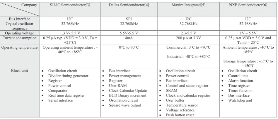
From the literature review, there are many design of RTC nowadays. Every RTC has their own features according to their specification to be use on any application. Even they have different features, they also have a similar part to make the RTC function correctly such as power supply, oscillation circuit, communication interface and many more. Fig. 1-4 shows a different RTC design from different company such as SII-IC Semiconductor, Dallas Semiconductor, Maxim Integrated, and NXP Semiconductor. The comparison in term of bus interface, block unit is tabulated in Table 1.
Fig. 1. RTC Block Diagram from SII-IC Semiconductor(S-35390A) [3].
Fig. 3. RTC Block Diagram from Maxim Integrated (DS3232) [5]
Fig. 4. RTC Block Diagram from NXP Semiconductor (PCF8563) [6]
Table 1 shows the comparison of different RTC from different company. As we can see from Fig. 1-4 and Table 1 some of them using I2C bus interface and some using SPI interface. This interface has their own advantage depending on their application. As for their oscillation frequency, all the RTC use the 32.768kHz crystal oscillator due to the stability of the crystal. This frequency is the most stable to be used in the RTC. The most important part on this comparison is their block unit. Even their block and design are different, but on every RTC, they must have the basic block that is oscillation circuit, bus interface, power management, register, frequency divider and counter. For this research, the part covered is on the logic part of the RTC that is bus interface, register, frequency divider and counter. The power management and oscillation circuit will be done by another researcher.
1.2 RTC counter increment flow
Fig. 5. Counter increment flow [7]
Fig. 5 show the increment of the counter on the RTC. Every 1Hz counter, it will represent 1 second of a real time. This increment will continue up until years. The seconds counter will count to 60 second then the minutes will increment by one. After the second reach exactly 60 second, the second counter will reset to 0. Then minutes counter will continue increase for 60 minutes. Then the hours will increment. After 24 hours, the date counter will increase. This increment flow will continue exactly as a real time until it reaches 1 years. After that it will
Company SII-IC Semiconductor[3] Dallas Semiconductor[4] Maxim Integrated[5] NXP Semiconductor[6]
Bus interface I2C SPI I2C I2C
Crystal oscillator
frequency 32.768kHz 32.768kHz 32.768kHz 32.768kHz
Operating voltage 1.3 V- 5.5 V 5.5V-5.5 V 2.3-5.5 V 1V – 5.5V
Current consumption 0.25 μA typ. (VDD = 3.0 V, Ta =
+25°C) 4mA 200 μA at 3.3V 0.25 μAat VDD = 3.0 V and Tamb = 25°C Operating temperature Operating ambient temperature :
-40°C to +85°C 0°C to 70°C Commercial: 0°C to +70°C Industrial: -40°C to +85°C
Ambient temperature : -40°C to +85°C
Storage temperature : -65°C to +150°C Block unit Oscillation circuit
Divider timing generator Register
Power control Comparator Real time data register Serial interface
Bus interface Power management Register User RAM
Clock Calendar Update BCD Binary increment Oscillation circuit Square wave output
Oscillation circuit Power control Bus interface
Control and status register SRAM
Clock and calendar register User buffer
Temperature sensor Voltage reference Push button reset
continue for the next year. The date will be depending on month and year as the month has different amount of days in every month and for leap years that will decide by the amount of days in February. This are the basic counter increment flow used to design this research RTC.
1.3 Advance Peripheral Bus
As for this RTC is dedicated to wireless microcontroller, this RTC needs to follow the bus protocol to be interface with the microcontroller. The microcontroller will use the Advanced Microcontroller Bus Architecture (AMBA) bus protocol. To easily interface the IP with microcontroller, the RTC need to match with Advanced Peripheral Bus (APB). APB is part of the AMBA hierarchy of buses. It is optimized to reduce the complexity of interfacing and for minimalize power consumption. The AMBA APB should be used to interface to any peripherals which not require high performance of bus interface and low bandwidth. The latest revision of the APB ensures that all signal transitions are only related to the rising edge of the clock. This improvement means the APB peripherals can be integrated easily into any design flow, with the following advantages [8, 9]:
• High-frequency operation
• Easy integration with cycle based simulators.
•It simpler to interface with new Advanced High-performance Bus (AHB)
Since this IP will be integrated with the microcontroller that using AMBA Bus Architecture, the RTC design then will follow the APB Specification as show in Fig. 6
Fig. 7. Propose block diagram of the RTC
Fig. 6. APB Standard for RTC [8,9]
The highlighted input/output pin is the important pin for the APB specification. The non-highlighted is not important and can be ignore if the RTC does not have that input/output pin. That pin also can be implement for additional features [8, 9].
2
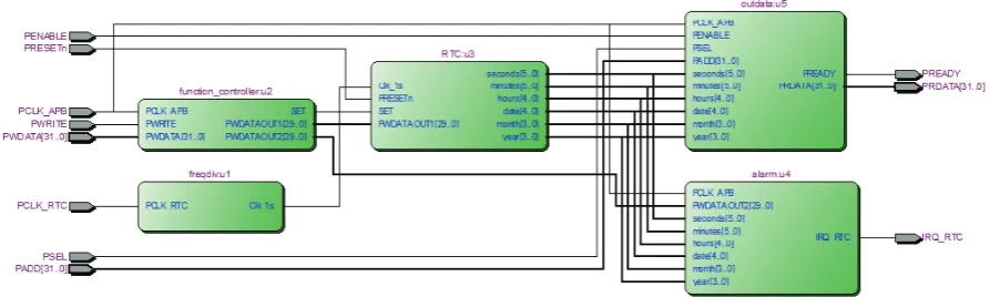
Propose RTC block diagram
Fig. 7 show the propose block diagram with bus interface which follow the APB Specification. The block diagram consists of bus interface, frequency divider, function controller, RTC, alarm and out data module. The RTC module is the module that will do all the counting and store the real-time value. The function of every module in the block diagram is explain in Table 2
Bus Interface
Out Data Module Function Controller Module
Alarm Module RTC Module
Table 2. Function of every module on the propose RTC
3 Full operation flows
Full flow of the RTC operation is as shows in Fig. 8. Firstly, the RTC will check for read and write data event. If there is data writing for manual set the time and date, the register inside the RTC module then will be overwritten by a new input value and will continue counting starting from the new value. If there is no writing data event or only the set alarm event occurs, the RTC will start counting from its initial value as stated in the flowchart. If reset is toggle, the RTC will goes into its initial condition that is 00:00:00 (hh:mm:ss) & 01/01/2017 (dd/mm/year). If not the current time and date value will be store into outdata module register. This value will be update and store for every 1 second. To read the data from the RTC, all the condition need to be meet which is the address is call, PSEL and PENABLE is toggle, then the date and time value will be
Fig. 9. RTL view of Top Module RTC
concatenated and transferred to PRDATA (output pin) in form of 32 data bit. For the alarm module, if the alarm is set, the alarm value will be compared with the real-time value. When the value is matched, an interrupt signal will be sent out to CPU as alarm signal.
Fig. 8. Flowchart of RTC operation
4
Result (Simulation and FPGA testing)
The developed RTC is simulated in Quartus II software. The functionality of the RTC is being test out from waveform simulation and testing on FPGA Board (Altera DE2-70). The RTL view of the Top Module RTC is as in Fig. 9.
UNIT FUNCTION
Frequency
Divider Generate 1Hz frequency from 32.768kHz Function
Controller To control function (e.g. Manual set time and date, set alarm)
RTC Generate time and date from counter and 1Hz frequency generated by frequency divider
Out data Store output data (32 bit) to be read (time and date value)
Table 3. PRDATA and PWDATA bit assignment
The Top Module of RTC consist of 5 sub-module that is frequency divider, function controller, RTC, alarm and outdata module. Their functionality is as stated on Table 2 before. 3 of the sub module will be running by APB clock that is function controller, alarm and outdata module. APB clock resolution is 62.5ns which is 16MHz. For frequency divider and RTC, it will be running by RTC clock source that is 32.768 kHz with
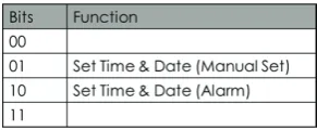
30.52μs resolution. The features that this RTC had is write data features (to manual set time & date and to set alarm). The data bit description for write (PWDATA) and read (PRDATA) is as shown in Table 3. The first two MSB bit of the PWDATA is used as a function bit that is to manual set the time & date and to set the alarm. For now, it only had two functions to be controlled. The function bit description is as shown in Table 4. For 00 and 11 bit function, this is reserved for future improvement features if need to be added.
Table 4. Function bit description
Lastly, the full RTC module then has been tested using FPGA Board (Altera DE2-70) with adding test module (red box in Fig.10) as a dummy input and the result is as shown in Fig. 11 (a)-(f). The dummy input description is as shown in Table 5. The LCD module is added to show the result on the LCD display of the FPGA Board.
Fig. 10. RTL view of Top Module RTC with added test module
Table 5. Sample input data used for PWDATA
Fig. 11(a-f) shows the LCD display result with their condition. Box below the LCD display show their input data.
PRESETn PENABLE PSEL PADD PWRITE PWDATA
0 0 0 0 0 Z*
Fig. 11(a). Condition: Reset (Initial condition)
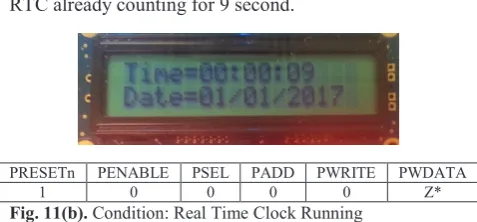
For Fig. 11(b), the condition shows the RTC running. Since the PRESETn is toggle to 1, the RTC will start counting from its initial value. The figure shows the RTC already counting for 9 second.
PRESETn PENABLE PSEL PADD PWRITE PWDATA
1 0 0 0 0 Z*
Fig. 11(b). Condition: Real Time Clock Running
When the PWRITE=1 and PWDATA sent a 32bit data, The RTC is on the writing event. Its either manual set or alarm is set. Fig. 11(c) shows the manual set time and date since the 32bit data sent is using 01 function bit to manual set as in Table 5(sample data input). When the PWDATA use the 10 function bit, it will set the alarm in the alarm module as shown in Fig. 11(d).
PRESETn PENABLE PSEL PADD PWRITE PWDATA
1 0 0 0 1 (1)*
Fig. 11(c). Condition: Manual Set (Date and Time)
PRESETn PENABLE PSEL PADD PWRITE PWDATA
1 0 0 0 1 (2)*
Fig. 11(d). Condition: Set alarm
Fig. 11(e) shows the interrupt signal is sent out. The interrupt signal is sent out because the alarm set (in Fig.11(d)) is already match the real time. So, the alarm is on.
PRESETn PENABLE PSEL PADD PWRITE PWDATA
1 0 0 0 0 Z*
To read the output data, The PSEL,PENABLE and PADD need to fill the requirement as stated in the operation flow. When the requirement is meet, the PREADY signal will be sent out and the PRDATA can be read is form of 32bit. The Fig. 11(f) shows that condition.
PRESETn PENABLE PSEL PADD PWRITE PWDATA
1 1 1 address 0 Z*
Fig. 11(f). Condition: IP is ready to be read (PRDATA can be read).
5 Conclusion
A logic part of real time clock is successfully developed and implemented on FPGA board with accurate time counter. This work will be improved in the future and then be continue to the layout level. After that, it can be integrated into the wireless microcontroller with the other IP to be fabricated. All the reference design and idea is referred from various application note and technical papers of conventional RTC [3-6,10-12].
This project is sponsored by Talent Corp. Malaysia in collaboration with Intel Malaysia and CEDEC USM. First of all, I would like to thank my supervisor, Dr. Shaiful Nizam Bin Mohyar for all his guidance and support throughout this project. I would like to thank my fellow friends, Farhah, Fira and Wang Hang Suan for outstanding support and helpful comment.
References
1. http://whatis.techtarget.com/definition/real-time-clock-RTC. (Accessed: 27- Jul- 2016)
2. https://learn.adafruit.com/ds1307-real-time-clock-breakout-board-kit/what-is-an-rtc. (Accessed: 27- Jul- 2016)
3. SII-IC Semiconductor, S-35390A, rev. 4.2, Datasheet (2016)
5. Maxim Integrated,” Extremely Accurate I2C RTC with Integrated Crystal and SRAM,” DS3232, Rev 5 (2010)
6. NXP semiconductor, “Real-time clock/calendar,” PCF8563, Rev.11 (2016)
7.
https://www.maximintegrated.com/en/app-notes/index.mvp/id/5791. (Accessed: 30- Apr- 2017)
8. AMBA specification 2.0, ed: ARM Ltd. (1999) 9. "Cortex-M System Design Kit Technical Reference
Manual," ed: ARM Ltd., (2011)
10. https://www.maximintegrated.com/en/products/digit al/real-time-clocks.html. (Accessed: 27- Jul- 2016) 11. Dallas Semiconductor,” 64 X 8 Serial Real Time
Clock”, DS1307, Datasheet
![Fig. 1. RTC Block Diagram from SII-IC Semiconductor(S-35390A) [3].](https://thumb-us.123doks.com/thumbv2/123dok_us/8125321.1353909/1.595.327.508.557.734/fig-rtc-block-diagram-sii-ic-semiconductor-s.webp)
![Fig. 6. APB Standard for RTC [8,9]](https://thumb-us.123doks.com/thumbv2/123dok_us/8125321.1353909/3.595.306.529.79.251/fig-apb-standard-rtc.webp)