Development of Real time Video/image
capturing and displaying architecture on
FPGA
1
Priya N. Gokani,
2Prof. Jignesh Joshi,
3Asst Prof. Jayesh R Chauhan,
4
Asst Prof. Payal G. Kheradiya
1,2,3,4Electronics & Communication Department, V.V.P. Engg College, Gujarat, India
ABSTRACT
Today’s Field Programmable Gate Arrays (FPGA’s) are in use to implement high performance image
processing systems. This paper proposes an implementation of a FPGA based digital camera system
for image capturing and real time image processing. For implementation of this image acquisition
system another two sub-system are interfaced with FPGA core. One of the sub-modules is CMOS
sensor for capturing the views of outside world and other one is digital graphical display for remote
viewing of captured image or video. These two sub-modules are bridged with help of FPGA. Main
role of this bridge in this implementation is to reframe the incoming data into displaying format. The
main goal of this proposed design is to implement and test advanced complex image processing
algorithm. Here proposed architecture has been developed on ALTERA’S DE II platform, which has
ability to communicate with a Personal Computer (PC) through an interfaced Joint Test Automatic
Generation (JTAG) for storing the images on to it and further processing.
Index Terms—CMOS camera, Color filter array (CFA), Field Programmable Gate Array
(FPGA), Graphical display, I2C interface, Pixel array scanning mechanism.
INTRODUCTION
Now a day’s FPGA technology impressively increases in the area of image acquisition for remote
controlling due to its fast response with very lower latency. The biggest advantage of this technology
is software programmable processor and hardware computing capability both can be developed within
outside. To fulfill this requirement solid image sensors are currently used are CCD and CMOS. Apart
from these two CMOS sensor technology is in leading stage because of it overcomes all disadvantages
of CCD sensor along with it reduces the size, power consumption of electric device(A). Because of its
high anti-radiation ability it is widely used in many atomized vision systems (A).
Currently there are many problems of remote visioning especially in real-time because of latency
period but by taking advantages of both FPGA technology and CMOS technology remote vision in
real time can be achieved at some remarkable level. So I had demonstrated an image and video
acquisition system with help of CLCLONE II EP2C35F672 FPGA which is provided by ALTERA
DE2 platform. This FPGA provides 33,216 logic elements, 8 MB SDRAM, 512KB SRAM, 4MB
Flash etc. The data capturing module used in this system is TRDB-DC2 which is 1.3 MP digital
camera and for displaying that TRDB-LCM digital graphical display is interfaced with
help of 40-pin header to the development board. Fig. 1 shows the image acquisition system with its
basic sub-systems. Here all the sub systems have been designed in verilog HDL (D).
.
Fig.1 CYCLONE II FPGA based data acquisition system
HARDWAREDESCRIPTION
I CMOS CAMERA SUB-SYSTEM:
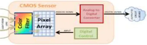
Generally the every CMOS camera accommodate following basic parts: the color filters the pixel
Fig.2 Basic component of CMOS camera system
As shown in diagram firstly the lens is used to configure all light rays to the sensor. In between of
lens and sensor array color filter array is used to capture color information. After the color filtering
process the light will be exposed on the each photo site of the sensor array and because of that some
voltage value has been generated from each photo site according to the exposure of light on it. That
output voltage is in analog format which has been multiplexed on single line and given to the ADC
for any kind of further data process, it may be on board or to other circuit board; so analog format has
been converted into digital format. So output of ADC is row digital data.
1. Color filter
Color filter is used to get the color information from the white light in every color camera system.
Now a day’s Bayer color filter array is a popular format for digital acquisition of color images
[1].Bayer filter pattern is an array or a mosaic of tiny color filters is placed over the pixel sensor array.
In this single particular color filter is placed on each pixel, One tiny filter corresponds to one pixel
from array. Due to this type of formation finally a color pattern array has been developed as shown in
figure in front of pixel sensor array.
FIG.3BAYER FILTER ARRAY
As shown in figure half of total no of pixels covered by green (g) filter, while another half part of
pixel array quarter part will be covered with blue (b) filter and another quarter part will be covered
as shown in sub-mosaic pattern. Sensor Scanning Mechanism: The CMOS camera sub-system
shown in Fig 2. Here CMOS sensor is MT9M011 consist pixel array of 1280*1024. Each pixel is a
photo site that will generate output voltage that is multiplexed on single channel. For proper scanning
of each pixel from an array, the scanning mechanism should be needed to develop on FPGA. For this
data capture controller has been designed in FPGA core. This controller provides a master clock
(MCLK) to sensor. Here whole system working on the clock mechanism and each operation has been
started with positive edge of clock.When sensor gets the master clock, it generates another three
scanning clocks that are pixel clock (PCLK), line valid clock (LVAL), and frame valid clock
(FVAL).According to this clocking mechanism capture controller will fetch the data of each frame
containing 1280 pixel in each row from the data line. Here data of each pixel is coded with 10 bits
because of 10-bit inbuilt ADC. This ADC provides digital row data. This digital row data is in Bayer
format because of using Bayer color filter array (CFA) before the sensor pixel array. This row data is
also called as sequential RGB. So to display this fetched data, sequential RGB or Bayer data will be
separated as 30-bit RGB on each channel. To reformat the Bayer row data into RGB the data of full
frame will be stored in linear buffer which is one kind of circular buffer so that real time processing
can be achieved. The I2C controller shown in fig 3.is used for serial communication which consist
two lines one for data transfer that is SDATA and another is serial clock SCLK for ynchronization.
With help of this data can be read or write into internal register of the CMOS camera.
.
FIG.4 SENSOR SCANNING MECHANISM
Fig.5 (a) code flow of scanning mechanism
Fig.5 (b) code flow of scanning mechanism
II Graphical display sub-system:
40 pin header of the ALTERA board. To grab the reformatted data from the FPGA LCD controller
(VGA controller) has to design in the FPGA core. This controller will provide proper display
synchronization signals to the display module. As shown in fig. 6 controller takes the RGB data from
SDRAM as shown in fig.1.along with this when pixel clock is arrived, controller generates horizontal
sync pulse clock (HSYNC), vertical sync pulse clock (VSYNC),data latch clock (DCLK), Global
reset (GRESTB), Shutdown control (SHDB) as shown.
Fig.6 TFT display sub-system
Here HSYNC and VSYNC are generated for Proper fostering of incoming row and column data
onto active area of raster in display module. Data clock is used to setup logic whether the incoming
data has to display on module or not, while global reset is used to reset all display register value to
zero.
1.Code flow of Data displaying mechanism:
As said to display data in an active region of raster the HSYNC and VSYNC are needed. To
generate these two signals from controller two counters has been developed that are H_Count and
V_Count as shown in fig,7 because here whole mechanism works on the pixel clock tick. According
to the specification of the display module data latching on active area logic has been developed.After
that color data latching mechanism has been develop with help of data clock enable /disable.Here
Fig.7 Code flow of Data displaying mechanism
III Results
In this paper, the domain under observation is incessantly supervised by capturing the video of the
area. With the help of the CMOS sensor, the capturing of video under observation is successfully
completed. This CMOS sensor will produce direct digital output because its associated circuit is
incorporated with 10-bit ADC. The mode register of the CMOS sensor is programmed with I2C
protocol, so that CMOS settings like resolution, exposure are configured with this protocol. The serial
data is assigned to the CMOS sensor which is obtained from the available parallel data. The data is
ceaselessly captured by the programmed sensor. CMOS sensor’s I2C interface and Pixel Data
interface are connected to the FPGA through GPIO interface of the DE2 Board. FPGA will have I2C
Slave controller module that will write the CMOS sensor configurable register values. In order to
restrain the stream of data coming from the sensor which is programmed to the memory, the IDFC
(Image Data Flow Controller) is used. This IDFC influences the stream of data to the memory.
Whenever the START signal is triggered then only the data is stored in the memory. It happens
continuously until STOP signal is found. This system consists of the black and white converter
module so that the data is laid in
in the pattern of black and white images only. ALTERA
memory. SDRAM controller is used to supervising these performances. The read & write signals are
rendered by SDRAM controller and it can also track which frame is being read or written. The video
can be monitored on a visual display unit such as an LCD monitor. For this purpose, the VGA
controller is used.VGA Controller module in the FPGA always reads the pixel data from one of the
ports of DDR SDRAM and it generates the required signals to display the video on the screen. Figure
8 shows real-time video capturing and displaying on the graphical display through CMOS camera
connected with ALTERA DE2 board.
Fig.8 proposed outcomes
REFERENCES
[1]. Bei Yan ,Yuefeng Sun,Fengfeng Ding,Haiwen Yuan.” Design of CMOS Image Acquisition
System Based on FPGA”, 2011 6th IEEE Conference on Industrial Electronics and Applications
[2]. Naga Raju Boya, Vijay Kumar Jinde, Bala Venkateswarlu Avvaru, Sreelekha Kande and
Ramanjappa Thogata,” Design and Development of FPGA Based Image Acquisition System”,
Indian Journal of Science and Technology, Vol 10(9), March 2017
[3]. Mohd. Ummaruddin, Prof. Mrs. G.M. Phade, Dr. Sanjay T. Gandhe, Prof. Pravin A. Dhulekar,”
Implementation of FPGA based Digital Camera System controlled from an LCD touch panel”,
2015 International Conference on Computing Communication Control and Automation
[4]. M. Petouris, A. Kalantzopoulos and E. Zigouris,” An FPGA-based Digital Camera System
Controlled from an LCD Touch Panel” ISSCS 2009. International Symposium on, 1-4
[5]. ALTERA “DE2 Development and Education Board User Manual “, Ver 1.08,2009
[6]. Terasic –LTM 4.3 Inch Digital Touch Panel Development Kit”, 2007
[7]. Altera, "Creating Low Cost Intelligent Display Modules with a FPGA and Embedded
[8]. Interactive Projection Game CSEE 4840 Project Design Document March 14, 2008
[9]. M V Ganeswara Rao “Implementation of Real Time Image Processing System with FPGA and
DSP” 2016 IEEE
[10].Chao LI, Yulin ZHANG, and Na Zhao ZHENG. Design of Image Acquisition and Processing
Based on FPGA[J]. 2009 International Forum on Information Technology and Applications,
2009, pp.113-115.
[11].Ning Li, and Junfa Wang. High-speed data acquisition system based on Camera Link [J].