University of Windsor University of Windsor
Scholarship at UWindsor
Scholarship at UWindsor
Electronic Theses and Dissertations Theses, Dissertations, and Major Papers
1-1-2007
A statistical reliability model for single-electron threshold logic.
A statistical reliability model for single-electron threshold logic.
Yanjie Mao
University of Windsor
Follow this and additional works at: https://scholar.uwindsor.ca/etd
Recommended Citation Recommended Citation
Mao, Yanjie, "A statistical reliability model for single-electron threshold logic." (2007). Electronic Theses and Dissertations. 6967.
https://scholar.uwindsor.ca/etd/6967
Single-Electron Threshold Logic
b y
Yanjie M ao
A Thesis
Submitted to the Faculty of Graduate Studies and Research through
Electrical and Computer Engineering
in Partial Fulfillment of the Requirements for
the Degree of Master of Applied Science at the
University of Windsor
Windsor, Ontario, Canada 2007
Library and Archives Canada
Bibliotheque et Archives Canada
Published Heritage Branch
3 9 5 Wellington Street Ottawa ON K1A 0N 4 C anada
Your file Votre reference ISBN: 978-0-494-34992-2 Our file Notre reference ISBN: 978-0-494-34992-2
Direction du
Patrimoine de I'edition
395, rue Wellington Ottawa ON K1A 0N 4 C anada
NOTICE:
The author has granted a non
exclusive license allowing Library
and Archives Canada to reproduce,
publish, archive, preserve, conserve,
communicate to the public by
telecommunication or on the Internet,
loan, distribute and sell theses
worldwide, for commercial or non
commercial purposes, in microform,
paper, electronic and/or any other
formats.
AVIS:
L'auteur a accorde une licence non exclusive
permettant a la Bibliotheque et Archives
Canada de reproduire, publier, archiver,
sauvegarder, conserver, transmettre au public
par telecommunication ou par I'lnternet, preter,
distribuer et vendre des theses partout dans
le monde, a des fins commerciales ou autres,
sur support microforme, papier, electronique
et/ou autres formats.
The author retains copyright
ownership and moral rights in
this thesis. Neither the thesis
nor substantial extracts from it
may be printed or otherwise
reproduced without the author's
permission.
L'auteur conserve la propriete du droit d'auteur
et des droits moraux qui protege cette these.
Ni la these ni des extraits substantiels de
celle-ci ne doivent etre imprimes ou autrement
reproduits sans son autorisation.
In compliance with the Canadian
Privacy Act some supporting
forms may have been removed
from this thesis.
While these forms may be included
in the document page count,
Conformement a la loi canadienne
sur la protection de la vie privee,
quelques formulaires secondaires
ont ete enleves de cette these.
All Rights Reserved. No P art of this document may be reproduced, stored or oth erwise retained in a retreival system or transm itted in any form, on any medium by any means w ithout prior w ritten permission of the author.
A bstract
As CMOS technology is predicted to reach its scaling limit in the next decade, vari ous nanometer-scale devices have been investigated for future nano-electronics. One promising candidate is Single-Electron Tunneling (SET) technology which has ben efits of its ultra-low power consumption and sub-nanometer feature size. However, shrinking device dimension has negative impact on reliability and results in increased device failure rates. In th a t case, reliability issue is becoming one of the biggest concerns in designing practical nanosystems.
I would like to express my sincere gratitude to my supervisor Dr. Chunhong Chen for his constant support, guidance and motivation.
I am grateful to the com mittee members Dr. Jessica Chen and Dr. Jonathan Wu for providing valuable feedbacks.
I would like to thank Ms. A ndria Turner and Ms. Shelby M archand for seamless adm inistrative assistance.
I would like to take this opportunity to offer my heart felt thanks to my affectionate parents: Yiming Mao and Enmei Shen for their endless support on my life and study.
Lastly, I would like to thank my dearest boy friend Yibo Zhou who is always by my side and has helped me to prepare the thesis.
v
C on ten ts
A bstract iv
A cknowledgem ents v
List o f Figures x
List o f Tables xii
1 Introduction 1
1.1 Limits of CMOS T echnology... 1
1.2 Introduction to SET Technology... 2
1.2.1 Theoretical B a c k g r o u n d ... 3
1.2.2 Fabrication L im ita tio n ... 5
1.3 Reliability Issue of SET T echnology... 7
1.5 Organization of T h e s i s ... 8
2 Threshold Logic G ate 10 2.1 Single-Electron B o x ... 11
2.1.1 Theoretical Background of Single-Electron Box ... 11
2.1.2 M athematics in Single-Electron B o x ... 12
2.2 SET Linear Threshold G a t e ... 17
2.2.1 M athematics on SET Linear Threshold G a t e ... 17
2.2.2 Circuit Examples for SET Threshold L o g ic ... 25
3 R eliability Issue on SET 33 3.1 Experiment on Reliability of 2-input NOR G a t e ... 34
3.1.1 Assumptions of the E x p e r im e n t... 34
3.1.2 Procedure of the Experiment ... 37
3.2 Statistical Model for G ate R e lia b ility ... 38
3.3 Reliability Model for O ther G a t e s ... 40
3.3.1 2-input NAND G a t e ... 43
3.3.2 K -input G a te s ... 43
4 Bifurcation Analysis for SET Logic Circuits 52
vii
C O N TE N TS
4.1 Bifurcation Analysis for Circuit Built out of NAND G a t e s ... 53
4.2 Bifurcation Analysis for Circuits Built out of 2-input NOR Gates . . 58
4.3 Bifurcation Analysis for Circuits Built O ut of K-input NOR G ate . . 59
4.3.1 Bifurcation Analysis for Circuits Built Out of 3-input NOR G ate 59 4.3.2 Bifurcation Analysis for Circuits Built Out of 4-input NOR G ate 60 4.3.3 Discussions on the K -input G ate ... 61
5 Future Work and A pplication 64 5.1 Energy E s ti m a t io n ... 64
5.2 Fast A lg o r ith m ... 65
5.3 Inputs C o rre la tio n s ... 66
6 Conclusion 67 A ppendix A: M ATLAB Programs for SET Experim ent 69 A .l Reliability Calculation for 2-input NAND G a t e ... 69
A.2 Calculation of a* of 2-input NOR G a t e ... 72
A.3 Calculation for r f of 2-input NOR G a t e ... 74
A.4 Stages of 2-input NAND G a t e ... 80
VITA AUCTORIS 87
List o f Figures
1.1 Power Extrapolation of Processors Following Moore’s L a w ... 3
2.1 Single-Electron B o x ... 11
2.2 Transfer Function of Single-Electron B o x ... 15
2.3 Transfer Function of Single-Electron Box when VjUmp » VriS e... 17
2.4 The N -Input Linear Threshold G a te ... 19
2.5 The N-Input Linear Threshold G ate Regresses to Single-Electron Box 21 2.6 The Equivalent Capacitance in Vx’s V ie w ... 21
2.7 Diagram of 2-input NOR G a t e ... 25
2.8 Simulation Result of 2-input NOR G ate by S I M O N ... 30
2.9 Simulation Result of 2-input NAND Gate by S I M O N ... 31
3.1 Noise on Capacitances and Islands of 2-input NOR G a t e ... 34
3.3 Reliability vs. Input Probabilities for 2-input NOR gate w ith 77 = 0.04 39
3.4 Reliability model coefficient 0:0(77) for 2-input NOR gate ... 41
3.5 Reliability model coefficient 0 1(77) for 2-input NOR gate ... 41
3.6 Reliability model coefficient 0 2(7?) for 2-input NOR gate ... 42
3.7 Diagram of 2-input NAND G a t e ... 42
3.8 Circuit of 2-Input NAND G ate in S I M O N ... 44
3.9 Reliability model coefficient /3q(tj) for 2-input NAND g a t e ... 45
3.10 Reliability model coefficient fti (77) for 2-input NAND g a t e ... 45
3.11 Reliability model coefficient (hiif) for 2-input NAND g a t e ... 46
3.12 3-Input NOR G a t e ... 47
3.13 3-Input NOR G ate Based on SET Threshold Logic ... 48
3.14 Simulation Result of 3-Input NOR G ate by S IM O N ... 49
3.15 4-Input NOR G a t e ... 50
3.16 4-Input NOR G ate Based on SET Threshold Logic ... 50
3.17 Simulation Result of 4-Input NOR Gate by S IM O N ... 51
4.1 The G ate Reliability at Different Stages of NAND G a t e s ... 57
4.2 Tendency of |<7'(a;)| in 2-input NOR G a t e ... 62
4.3 Tendency of \h'(x)\ in 3-input NOR G a t e ... 63
xi
List o f Tables
1.1 Param eters of Process Adhered to Moore’s L a w ... 2
1.2 Some Single-Electron Transistors [8] ... 6
2.1 T ruth Table for 2-input NOR G a t e ... 25
2.2 TVuth Table for 2-input NAND G a t e ... 32
3.1 Variables in Normal Distribution ... 37
3.2 Estim ated reliability r for 2-input NOR gate with t] = 0 . 0 4 ... 38
4.1 Hardware and Software Environment of the E xp erim ent... 62
Introduction
1.1
Limits o f CMOS Technology
Complementary metal-oxide-semiconductor (CMOS), is a major stream of integrated circuits in the recent years. During the past 25 years, Si-CMOS technology has been advancing along an exponential path of shrinking device dimensions and increasing packing density simultaneously. However, the original premise of the Moore’s law reveals th a t integrated circuits will double in transistor counts every 18 to 24 months [1]. We take processor as an example, if it sustains the growth model in Table 1.1, the processor manufacturers would reach beyond a billion (109) transistors per processor core by 2007. The level of this development is not possible for today’s CMOS manufacture techniques [2]. Even with the deployment of CMOS transistors
1
I. IN TRO D U C TIO N
Table 1.1: Par,im eters o Process Adhered to Moore’s Law
Process Name P856 P858 Px60 P I 262 P I 264 P1266 P1268
1st Production 1997 1999 2001 2003 2005 2007 2009
Lithography 0.25//m 0.18/im 13/im 90nm 65nm 45nm 32nm
G ate Length 0.20/xm 0.13/mi <70nm <50nm <35nm <25nm <18nm
Wafer Size(nm) 200 200 200—300 300 300 300 300
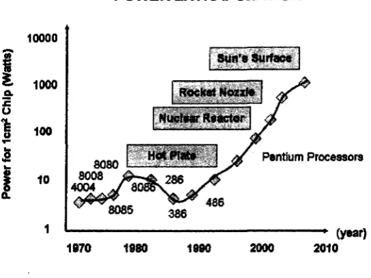
in large numbers, the future development of traditional CMOS transistors is not possible to be carried out due to increasing power consumption concerns as well. As depicted in Figure 1.1, to maintain exponential growth in packing density, the next- generation Pentium would literally require as much power for operation as a nuclear reactor in size comparative analysis. In such a state of affairs, the continued success of the electronic industry will increasingly depend on emerging nanotechnologies which have advanced rapidly in the recent past and has shown potential for large scales of integration, specifically of an order of a trillion (1012) devices in a square centimeter. Various nanometer-scale devices, such as single-electron tunneling transistors (SETs), resonant tunneling diodes (RTDs), and quantum dots and quantum cellular autom ata (QCA), have been investigated for future nanoelectronics epoch. In this thesis, we are focusing on Single-Electron Tunneling (SET) technology which has been extensively investigated for ultra-low power consumption and sub-nanometer feature size. So far, many SET-based circuits have been experimentally demonstrated.
1.2
Introduction to SET Technology
POWER EXTRAPOLATION
I
a. U 01
10000 1000 100 10 Pentium Processors 8080 8008 4004 286 486 8085 386 Sun's Surface Hot Plats Racket Nozzle Nuclear Reactor (year)1970 1980 1990 2000 2010
Figure 1.1: Power Extrapolation of Processors Following Moore’s Law
the replication of feat in the solid state took until the late 1980s. Early theoretical work was done by Ben-Jacob and Gefen (1985) [3], Likharev and Zorin (1985) [4], and Averin and Likharev (1986) [5]. In 1987, Fulton and Dolan of Bell laboratories first dem onstrated the feasibility of SET device [6]. Today, there is a standard procedure to build a single-electron transistor with a double angle evaporation method in the
A l/A lO i material system [7].
1.2.1
T heoretical Background
A fundamental understanding of single-electron devices can be achieved by electro static in the statics. Supposing an electron is positioned closely to an uncharged m etal sphere (called an island), it would feel a repulse force from the sphere. Here, the net charge Q of the system consisted of island and the electron is -e. Although
3
1. INTRO D U CTIO N
the fundamental charge e = 1.6 x 10~19 is very small on the scale of human being, it is rather strong for nanoscale. Assuming the sphere is ln m in radius and surrounded by vacuum, the surface electric field would be remarkably large as 14MV/cm. This electrostatic repulsion is called Coulomb Blockade.
The necessary condition to observe single-electron phenomena such as Coulomb blockade is
E c = ^ > kBT (1.1)
where kB is Boltzmann’s constant (kB = 1.38 x 10~23m 2kgs~2K ~ 1), T is the absolute tem perature, C is the total capacitance of the charged island, and e is the elementary charge (e = 1.6 x 10~19). E c, here, is called Coulomb energy.
It is obvious th a t the characteristic capacitance of a single-electron system has to be quite small for operation a t room temperature. Assuming T = 300A” (room tem perature), according to Equation 1.1,
E c = > kBT =4> C <
2C 2kBT
(1.6 x 1 0 -19)2 2 x 1.38 x lO" 23 x 300 = 3 x 10-18
= 3(aF)
( 1.2)
1. IN TRO D U C TIO N
The structure of Single-electron tunnel circuits normally consists islands, tunnel junctions, capacitors and ideal driven voltages. Electrons tunnel independently from island to island through tunnel junctions. The tunnel resistances must be larger than the fundam ental resistance in order to localize the electrons on islands.
L
Rt > R q = - j « 25813Q (1.3)
where h is Planck’s constant (h = 6.626068 x 10~34m 2k g /s).
An electron tunneling through a junction in the quantum scale is a stochastic process. If we define Perror as the probability th a t the desired transport does not occur, the switching delay can be expressed as:
In
(P error)QbRt“ ~ v ; \ - V c " (L4)
where R T is the tunnel resistance.
1.2.2
Fabrication Lim itation
Over the past few years, there has been rapid progress in the fabrication of the single-electron devices. Table 1.2 shows some single-electron transistors with different manufacture methods.
Nevertheless, the technology of fabrication of single-electron devices is still in its infancy. There is still a large gap between the laboratory and industry fabrication.
Implementation of SET devices requires a fabrication of very small conducting particles, and their accurate positioning with respect to electrons. However, the
5
1. IN TRO D U C TIO N
Ta die 1.2: Some Single-Electron Transistors [8]
Materials (Island, Barrier)
Fabrication Method
Al, A lO x Evaporation through an e-beam-formed mask [9] CdSe; organics Nanocrystal binding to prepatterned Au electrodes [10]
A l\A lO x Evaporation on a Si^N ^ membrane with a nm-scale orifice [11] Ti; Si M etal deposition on prepatterned silicon substrates [12] Carboran molecule E-beam patterned, thin-film gate; STM electrode [13]
Si; S i 0 2 E-beam patterning + oxidation of a SIMOX layer [14]
Nb, NbO x Anodic oxidation using scanning probe [15]
technology for tight control of dimensions is not achievable a t present. Although current nano-fabrication technologies have made possible small SET devices, the time for fabricating large SET circuits is still expected to be several decades away.
Further more, largely uncontrollable charge fluctuations, so-called random back ground charges, are a major obstacle for real world applications. Impurities and trapped electrons in the substrate induce charge on islands. Those unexpected charges usually destroy the correct function of the device. A single impurity electron located in an unanticipated position is possible to change the desired device behavior. As far as today’s processing techniques, it is not able to control the purity of materials enough to meet conditions suitable for SET device production.
1.3
R eliability Issue o f SET Technology
Nano-scale devices are more sensitive to a variety of random noises including the SET devices. As mentioned above, it is imagined th a t certain amount of charges (random background charges) would appear on nodes of SET devices during the fabrication process. These charges generate a biased voltage contributing to the total voltage across the SET device. The logic behavior could fail in th a t event and the circuit becomes less reliable. For th a t reason, reliability turns to be one of the biggest concerns in designing practical nano-systems.
Progress in research work on reliability issues of nano-electronic circuits involves two aspects. One is reliability evaluation and analysis. The other one is reliability improvement.
Reliability analysis refers to techniques for estimating circuit reliability, or finding acceptable error bounds of individual devices for reliable operation of the overall circuit. Among these techniques are Markov model [17], Markov random fields (MRF) [18], Bayesian formalism [19], probabilistic transfer m atrix (PTM ) [20], probabilistic gate model (PGM) and bifurcation m ethod [21].
Reliability improvement, on the other hand, is to use various architectures or new encoding techniques for increased reliability. Modular redundancy is such a typical example [22] [23].
1. IN TRO D U C TIO N
1.4 A N ew Statistical Reliability M odel of SET
Technology
In most previous work, people analyze the reliability of SET circuit by assuming a constant value of failure rate which is not suitable in practise. The incorrect as sumptions lead to an improper result, and then turn into an inaccuracy guidelines for circuit designers.
In this thesis, we evaluate the reliability of SET-based logic gates by presenting a statistical model which takes into account the process variations (especially random background charges) and input patterns. By indicating the reliability of a gate is not independent of other gates in the circuit bu t affected by all its fan-ins, we set up a relationship between process variations and the error bound for reliable opera tions. Those results serve as an im portant line for researchers and circuit designers. Moreover, the general method can be applied to other gates and other nano-scale technologies although only SET-based 2-input NOR and 2-input NAND logic gates are discussed in this thesis.
1.5
Organization o f Thesis
The organization of this thesis is as follows.
C hapter 2 is focused on the design of threshold logic functions in SET logic gates with the tunnel junctions’ specific behavior. The linear threshold logic gate’s stru ctu re
C hapter 3 is devoted to the experiment of reliability of 2-input NOR gate and 2-input NAND gate. Given two assumptions of process variations and correlation of the two inputs, we conduct a particular experiment to see how the reliability of the 2-input NOR gate and 2-input NAND gate depend on random noises as well as input patterns. In the later part of the chapter, we propose our statistical model of 2-input NOR gate and 2-input NAND gate from the regression method, followed by the discussion on K -input gates.
In C hapter 4, bifurcation analysis is provided for finding out the error bound of 2-input NAND gate and 2-input NOR gate. K-input gates and time complexity of the experiment are discussed later.
C hapter 5 comments on the future work and applications.
C hapter 6 is the conclusion part.
C hapter 2
Threshold Logic Gate
Originally, Threshold Logic Unit is an idea from neuron network as the origin of artificial neuron. It is first proposed by Warren McCulloch and W alter P itts [24] in 1943. It employs a threshold or step function taking on the values of 1 or 0 only.
out
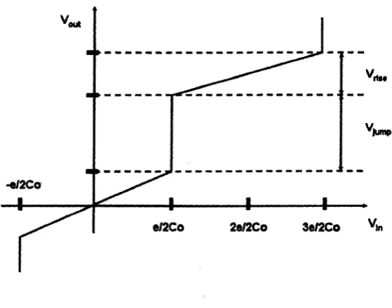
Figure 2.1: Single-Electron Box
2.1
Single-Electron Box
The so-called Single-Electron Box is an example of electrons tunneling. It consists of a tunnel junction in series with a true capacitor. The single-electron box has been the subject of numerous experimental and theoretical research, since it is a good circuit element to exhibit Coulomb blockade phenomena. The first experimental realization of a single-electron box was achieved by Lafarge et al [25].
2.1.1
T heoretical Background o f Single-Electron B ox
In Single-Electron Box, the tunnel junction is considered as a leaky capacitor. An electron needs an adequate energy or voltage threshold to tunnel from one plate of the capacitor to the other side. The critical voltage in Figure 2.1 is a judgement to decide weather the tunnel event is possible.
Suppose the tunnel junction with a capacitance of Cj and the remainder of the circuit has an equivalent capacitance of C0 in the C /s perspective. The critical voltage
Vc for the junction is:
l l
2. THRESHOLD LO G IC G ATE
Vc 2 (Cj + Ce) (2' 1}
In Equation 2.1, as well as in the remainder of this discussion, the charge of the electron is referred to as e = 1.6 x 10~19. Strictly speaking, it is not correct since the quantum of an electron is a negative value. However, it is much more convenient to consider it as positive. In this thesis, th e true negative value is only taken into consideration when talking about the direction of the tunneling.
Generally speaking, if we define the voltage across a junction as Vj, a tunnel event will occur through this junction if and only if
\V j\> V c (2.2)
If |Vj| < Vc for all junctions, the tunnel event cannot occur. We call th a t the circuit is in a stable state. The voltage of each component is resulting from the dissipation of the input voltage source, so each stable state determines a new output value. We restrict the number of possible stable states to two ( “1” and “0” or “ON” and “O FF ”) based on the Boolean input and output logic we are using in our research.
2.1.2
M athem atics in Single-Electron B ox
In Figure 2.1, the node (island) between the tunnel junction Cj and the true capacitor
C0 is considered as a node containing j electrons.
electrical equilibrium. If j is smaller th an 0, j electrons were removed from the island. Since the electron has a negative charge, j < 0 means th a t a positive charge is present on the island. O ther if j > 0, j electrons were added to the island, and there is a negative charge present on the island.
The critical voltage Vc of the tunnel junction can be expressed as:
The voltage Vj (Figure 2.1) across the tunnel junction is:
V-VJ — = Vy%n • __ ^1 1 T ^ sy I ___ = n ri-— nC° I n + ___ t- n —3 _______ n V"1*) (2 4)
Cj + C0
Ci + Co Cj + Co Cj + Co
In Equation 2.4, the first item is due to capacitive division of the input voltage V*n over the capacitances Cj and C0. The second item is the voltage resulting from the
j e charges on island divided by the to tal capacitance between the island and ground.
The output of the circuit is:
V ^ - V i n ^ - c j'+ C o Cj + Co (2-5)
The circuit is in a stable state when \Vj\ < Vc. Combining Equation 2.3 and Equation 2.4 leads Equation 2.6.
13
2. THRESHOLD LOGIC GATE
n\<V.
-*■ I ^ # T +
je
C j + C 0 Cj + Co' 2(Cj + C0)
® . ^inCo . J®
< -r
2(Cj + C0) Cj + C0 Cj + C0 2(Cj + C0)
. e - . 2i e < y < e ~ 2J'e (2 6 )
2 Co m 2 C0 [ }
Therefore, for any value of Vin, th e circuit could reach a stable state with specific
j satisfying the above relation.
T he gradual increase or decrease of the input voltage Vin from a stable state leads a similar increase or decrease of the output value in the circuit. Supposing the input voltage Vi„ increases from zero, th e voltage across the junction Vj will eventually reach the tunnel event point when its absolute value is larger than Vc. In this case, an electron tunnels through the junction from one plate towards the other side. For a positive input voltage, the electron always tunnels away from island, resulting in a sudden increase of the island voltage (V^t). For a negative input voltage, the electron always tunnels towards island, resulting in a sudden decrease of the island voltage ( V o u t ) .
The Vout ~ Vin transfer function is displayed in Figure 2.2. Here, the sudden change in output voltage is referred to as
Vjump — q q (2.7)
T h e in creasin g v o lta g e range corresp on d in g to a sta b le s ta t e is
out
-«/2Co
e/2Co 2e/2Co 3e/2Co
Figure 2.2: Transfer Function of Single-Electron Box
The detailed calculation is as follows:
According to Equation 2.6
j = 0 = *
V n it,j
=0
- e _e_
2C0 < in < 2C0
c<
j = - i
a + c ,
e 3e
K n
2C0 Cj
Cj + C0 Vin + Ci + C0
(2.9)
(2.10)
15
2. THRESHOLD LOGIC GATE
T he Vjump and Vrise axe calculated as follows:
Vjump
Vrise
The ratio of Vjump and Vrise is
e
Vjump Cj + Ca C0 /r)1
Vise “ C fi ~ Cj {2-13)
Co(Cj + C0)
If Vjump Vrise, the transfer junction curve regresses to a shape of a staircase. In th a t condition, C0 3> Cj.
The shaxp discontinuities of the staircase transfer function of Single-Electron Box indicate two facets. They are key points for creating a bridge between threshold logic theory and single-electron tunneling technology.
First, if the input voltage is limited to an small area around a discontinuity point, the point can be used as a threshold.
Second, if we apply an additional voltage to bias the circuit so th a t its state is
clo se to a d isc o n tin u ity p o in t, o n ly a small voltage can generate a large swing in the
output voltage as an amplifier. The ratio over the output and the input is called amplification factor.
V (o u t,j= -l,V in =e/2C0) ~ V(out,i=0,Vrin=e/2C o)
e Ci + C0
= V ( o u t j = _ i y i n = 3 e / 2 C „ ) ~ V ( o tlt , j = _ l , V j n = e / 2 C o )
Cj 3e
+
CiCj + C0 2C0 Cj + C0 Cj + C0 2C0 Cj + C0 Cj&
C0(Cj + Co)
(2 . 11)
-ettCo
2e/2Co
rf*»
Jump
Figure 2.3: Transfer Function of Single-Electron Box when VjUmp » Vrise
Given the characteristics of the Single-Electron Box, we can extend this circuit to perform linear threshold logic.
2.2
SET Linear Threshold Gate
2.2.1
M athem atics on SET Linear Threshold G ate
Threshold logic gates are devices which are able to compute any linear separable Boolean function relying on the following equations. These equations are derived from th e step function in threshold logic unit in neuron network. The output G (x) of this transfer function is binary of 1 and 0, depending on whether the input meets a specified threshold. If the operation meets the threshold, the output is set to be one. Otherwise, it is zero.
17
2. THRESHOLD LOGIC GATE
G (x) = sg n {F {x)} = < 0 if F (x ) < v ' 0 , (2.14)s 1 if F (x ) > 0
F (x ) ~ u& i ~ ^ (2-15)
where x* is the Boolean inputs and is the corresponding integer weights.
T he linear threshold gate performs a comparison between the weighted sum of the inputs ]Cr=i and the threshold value ip. If the weighted sum of inputs is greater or equal to the threshold, the gate produces a logic being 1. Otherwise, it is 0.
Single-Electron Box discussed in the previous section is following this threshold behavior. From the clues of the two indications mentioned above, the strong dis continuity point is referred to the gap between one stable state and its neighboring state. We choose two neighboring states and the discontinuity point between them. The circuit operation point is set to be in the area of the discontinuity point. The circuit can only produce two distinct values. By setting a threshold between these two values, we can make these two 1 and 0.
We choose V*n = e/2C 0 (Figure 2.3) as the discontinuity point and employ V~
and V + for the two desired values. The values of V ~ and V + are V~ = Vrise « 0, and K+ ljump.
Broadly speaking, the weights (u/j) associated with the inputs of the linear thresh old gate should be allowed both positive and negative values. However, most current implementations of the linear th resh old g a te o n ly allow for p o sitiv e w eig h ts [27] [28].
c as
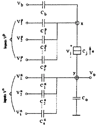
Figure 2.4: The N-Input Linear Threshold Gate
Figure 2.4 is the main structure of threshold linear logic which is implemented with Single-Electron Box as basis (Equation 2.14 and Equation 2.15). The basic two ele ments tunnel junction Cj and output capacitance Ca are adopted from Single-Electron Box. The input voltages V p = { V f, V2 , ..., V p} are weighted by their corresponding capacitors Cp = {Cf, C%,..., Cp}. The composite output is an added voltage across the tunnel junction. The input voltages V n = {V", V2n, ..., V ?} are weighted by their corresponding capacitors C n = {C” , C2 , ..., C"}. The composite output is a subtract voltage across the tunnel junction. Since the tunnel junction voltage Vj should be larger th an the critical voltage Vc, we set a biased voltage Vb with the corresponding weight Cb to adjust it in order to meet threshold value ip.
For the purpose of making the following discussion clear and readability, we set the following notations from Lageweg’s paper [26].
19
2. THRESHOLD LOGIC GATE
r
C i = c , + £ c j (2.16)
fc=l
3 3
(2.17)
Cr = C ^C j + CgCg + C jC l (2.18)
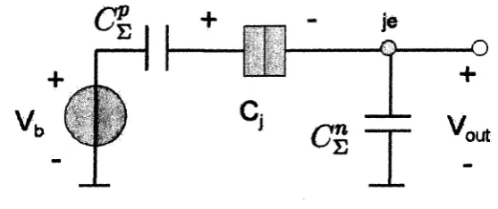
Then Figure 2.4 regresses to Figure 2.5 which looks like Single-Electron Box. It is a circuit with a series of capacitors Cg, Cj and Cg. The CT is the sura of each two item s’ product.
To evaluate of this circuit, Vc is needed to be calculated first of all. According to Equation 2.3, we get Vc in this case. From C j’s perspective, Cg and Cg are parallel and the equivalence of these two capacitors are
We refer the voltage at node x as Vx. According to the Figure 2.6, the composite of the input voltage V p and the biased voltage Vj on voltage Vx is
The composite of the input voltage V p and the biased voltage Vb on the V) across tunnel junction is
(2.19)
Vx(Vb, V p) =
{Cj
+
cg)(cbvb
+ E L i
civ*)
C r
je
-Q - ■O
c i
V,
outFigure 2.5: The N-Input Linear Threshold G ate Regresses to Single-Electron Box
F ig u re 2.6: T h e E q u ivalen t C a p a cita n c e in Vx ’a V iew
2. THRESHOLD LOGIC GATE
Vj(Vb, V p) =
cg(cbvb
+ ELi
<%}%)
C r
(2.22)
The composite of the input voltage V" on the Vj across tunnel junction is
Combing Equation 2.22 and Equation 2.23 leads to the composite of Vb, V p and
V n on Vj across tunnel junction is as follows:
As we talked before, the activity about the electron is determined by the com parison of Vj and Vc. If Vj > Vc, the electron will tunnel in the arrow’s direction in Figure 2.4.
Presently, we could formulate the function F (x ) in Equation 2.15 for the imple m entation of SET linear threshold logic.
CT CT CT (2.24)
F (x) = Vj(Vb, V p, V n) ~ V c (2.25)
Since we only focus on th e sign of F (x ), we simply ignore CT .
fc=i fc=i
We take p art of F (x ) as i/j
F ( i ) = C l £ C t K - C£ £ W + C tfh V , - i (C5 + Cg)e (2.27)
r
5(2.28)
^ = ^(C g + C S J e - C g C M (2.29)
Comparing Equation 2.15 and Equation 2.28, we find th a t the corresponding weights Ui are realized as C n or Cp. To be more precise, the positive uh is realized as
Cp (p means positive); the negative w, is realized as Cn (n means negative). W h at’s more, F{x) has nothing to do w ith th e junction’s capacitance.
In th e same way, the inputs Xi are realized as V n or V p. To be more precise, the positive Xi is realized as V p (p means positive); the negative x t is realized as Vn (n
means negative).
Equation 2.29, indicates th a t the threshold is affected by the biased voltage Vb(b
means biased) and biased capacitance
Cb-To sum up, the presented circuit depicted in Figure 2.4 implements an n-input linear threshold gate. The circuit is consisted of one external voltage (Vb) and n + 2 true capacitors (n input capacitors, Cb and C0) and the corresponding positive and
n e g a tiv e in p u t volta g es.
After finishing talking about the structure of the threshold logic circuit, we change our views to the output value.
23
2. THRESHOLD LOGIC GATE
If one electron tunnels through the junction in the arrow’s direction (Figure 2.4), it increases a —e voltage on node x (Vx). The effect is
6VX = ~ e ( Q + (2.30)
Cr
Sqx = - e (2.31)
Due to th e voltage division, th e changed voltage on V0 is
- p
P-6V0(x) = (2.32)
8qx = - e (2.33)
Likewise, when one electron tunnels through the junction in the arrow’s direction (Figure 2.4), it increases a +e voltage on node y (V^). The effect is
SV0(y) = e(CJ + .CS). (2.34)
c T
Sqy = e (2.35)
To sum up, if one electron tunnels in the arrow’s way, the composite effect on the output voltage V0 is
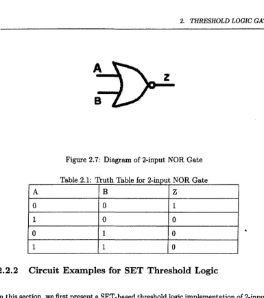
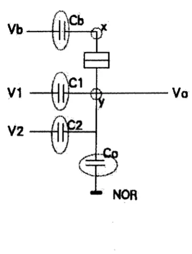
Figure 2.7: Diagram of 2-input NOR G ate
Table 2.1: T ruth Table for 2-inpu ; NOR Gate
A B Z
0 0 1
1 0 0
0 1 0
1 1 0
2.2.2
Circuit E xam ples for SET Threshold Logic
In this section, we first present a SET-based threshold logic implementation of 2-input NOR G ate (Figure 2.7). The 2-input NAND Gate and K-input gate will be discussed later. By using threshold logic, the 2-input NOR gate can be implemented with four capacitors (C\, C2, Cb, C0) and one tunnel junction in two level logic (0 and 1).
The tru th table for 2-input NOR gate is Table 2.1 by supposing the two inputs are A and B and the o utput is Z .
The corresponding equations are as follows:
25
2. THRESH O LD LOGIC G A TE
z — sg n {—a — b + 0.5} (2.37)
W hen assigning values to th e components in the circuit, we assume the ratio of the capacitors could realize the input weights (u>i). Comparing Equation 2.37 and Equation 2.28. We get the following relations for the weights
C l = 0 (A: = 1,2,...) (2.38)
C f C f = e y e * (2.39)
C | = Cb (2.40)
C£ = C r + C J + Co (2.41)
Therefore, we get the relation w ith C f and C f
C \ = C l (2.42)
It is easy to understand, since the two inputs are equivalent in logic.
We follow Lageweg’s unit capacitance [26], and set the capacitances C f and C f the same with his.
where l a F = 1 x 10 18F.
C f = 0.5aF
C l = 0.5aF
T he output capacitance C0 is
C0 = 9 aF (2.45)
The biased voltage V& is set as 16mV for the simplification and practice.
y6 = = 0.0167 = 16mV (2.46)
la F
To correspond with Vb, the inputs A being 1 (Vi) and B being 1 (V2) are also set as 16mV.
V-i = = 0.016V = 16m V (2.47)
1 aF
V2 = = 0.0161/= 16m V (2.48) 1 a r
By observing the tru th table, we find th a t when A = B — 0, the output Z = 1. In other words, F (x ) > 0.
We can calculate the F ( x ) in th a t case, after substituting the capacitances and voltages we have set.
27
2. THRESHOLD LOGIC GATE
F (C " = C2" = 0.5 aF, CQ = 9 aF, V? = VJ* = 0, Vb = O .le /la F )
= -c6(crif + c2
"i/2n) - l(a + cr + cr + c0)e + (cr + c2
n + c0)c6h
= —Cb x 0 — ^ ( ^ 6 0.5aF -h 0.5a/ '1 + 9 d ^ )c
s
+(0.5a F + 0.5aF + 9aF ) x Cb x O.le/1 a F > 0 (2.49)
= * Cb > 10a F (2.50)
If there is one input being 1, for instance, A = 1, the output is going to be Z = 0. So F (x) < 0
F (C " = C2" = 0.5aF, C0 = 9aF, V? = O .le/la F , V2n = 0,Vb = 0 .1 e /laF)
= G S 2 c t V ? - ( ^ £ W - l ( C ? + ^ ) e + C?
k
=1
fc=l
=
-cb(civr+c%v2n) - \(cb
+cr+cr+
c
0
y
+ (cr+cr+
c
0
)cbvb
= - C b X (0.5a F x 1) - h c b + 0.5aF + 0.5aF + 9aF)e
s
+ (0 .5 aF + 0.5a F + 9a F ) x Cb x 0.1e / la F < 0 (2-51)
=t> Cb < 11.11 o F (2.52)
Thus, for the function 2-input NOR gate, Cb has to be picked up from
Finally, we choose
cb
=
1(10 + 11.11)*
10.6 (2.54) AOnly when the value of the Cb is in the above range, the circuit works as a 2-input NOR gate. Due to the manufacture problems, the Cb could not be accurate but has a deviation. Since the deviation is supposed to be equivalent for the positive and negative side, Cb is chosen as the middle value in the range, which makes it more tolerant. The following Cb for the other gates is chosen following this law as well.
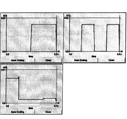
To verify the param eters, we use SIMON as Figure 2.8. T he two in the first line provide the two inputs A and B. And, the third one verifies the output Z.
The curves in Figure 2.8 correspond to the Table. 2.1 very well.
So far, we have had all the inputs and capacitance values for the 2-input NOR gate. T he conclusion is as follows.
Vb = 16 m V
C\ — C% = 0 .5 a F , C0 — 9aF, Cb = IO.60F
Cj = 1.0 aF, R j = lOOfcO (2.55)
where the value of Cj and R j are adopted from SIMON. These param eters are called standard values for the following discussion.
We do the similar procedure and get the values for 2-input N A N D gate. Different
from the 2-input N O R gate, When A = B = 1, the output value is Z — 0, otherwise, it is Z = 1.
29
2. THRESHOLD LO G IC G ATE
M l
Santa Scaha IOC
w on
HM
«**#*
*
JlSlifillt llllhlfilll
...1 ■ ■ ^
mm
Sum Scaling______| Om»
ft* ft*
, StoRMt ■.
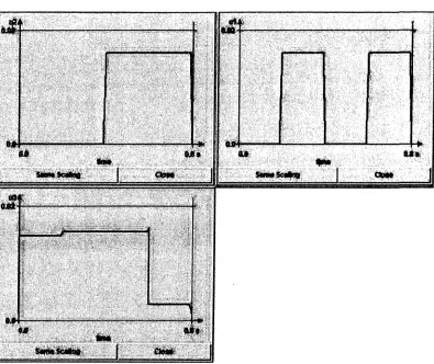
Figure 2.9: Simulation Result of 2-input NAND G ate by SIMON
31
2. THRESH O LD LO G IC G ATE
Table 2.2: T ruth Table for 2-input NAND G ate
A
B
z
0
0
1
1
0
1
0
1
1
1
1
0
The corresponding equation is
z = sg n {—a — b + 1.5} (2.56)
For the 2-input NAND gate, we use SIMON as in Figure 2.9. Table 2.2) provides the tru th table of 2-input NAND gate.
Reliability Issue on SET
A variety of nano-scale devices are currently being used to design digital logic. How ever, the random noises (such as process variations and random background charges) and physical failures with devices and interconnects may lead to faulty logic behav iors. W hen this happens with a wrong logic output, the logic gate is said to fail. If a logic gate has a failure probability e, it is said to have a reliability r, where r = 1 — e. In this section, we look at the reliability model for SET-based logic gates by showing the process of experimentally obtaining their reliability. The proposed model turns out to be approximate with statistical nature.
33
3. R E L IA B IL IT Y ISSUE ON S E T
Vb
V1
Vo
V2
b C p
NOR
Figure 3.1: Noise on Capacitances and Islands of 2-input N O E Gate
3.1
Experim ent on Reliability o f 2-input N O R Gate
3.1.1
A ssu m p tions o f th e E xperim ent
As mentioned before, the reliability is not a constant value but varies with the en vironment. In order to see how th e reliability of the 2-input NOR gate depends on random noises as well as input patterns, we conduct a particular experiment with the following two assumptions.
The assumption is based on the central limit theorem, which is a set of weak- convergence results in probability theory. It states th a t if the sum of the variables has a finite variance, then it will be approximately normally distributed, following a normal distribution. Since many real processes generate distributions with finite variance, this reveals the universality of the normal probability distribution.
The probability density function of the normal distribution is
/ ( w ) = (!U )
where z is a random variable.
In case of capacitance, z is a random value of capacitance with mean // being its standard value.
In case of islands, z represents the value of random background charge with mean
fj, = 0. The value of a can be selected based on the varying range of random variable.
The normal distribution function is effective from negative infinity to positive infinity. In industry, we choose p art of this function instead of the whole one.
In Figure 3.2, about 68% of values drawn from a standard normal distribution are within 1 standard deviation ( la ) away from the mean; about 95% of the values axe within two standard deviations (2a) and about 99.7% lie within 3 standaxd deviations (3a). T h at is so-called 3a control limit, which is broadly used in industry.
Suppose the noise on the capacitance is within the range ±77 x 100%, which means the capacitance is picked up during the range [Cst<i - rjCstd, C3td + r]Catd\ following the normal distribution. According to the 3 a control limit,
35
3. R E L IA B IL IT Y ISSU E O N S E T
Figure 3.2: 3a control limit
±r) x 100% x Cstd = i 3 x <rc
ac = ^ (3.2)
where Cstd is the standard value of capacitance.
In case of the islands, we set the noise is within the range ±77 x e, and the random background charge on the island is within [—rje, rje], so
±77 x e = ± 3 x <re
*e = f (3-3)
Table 3.1: Variables in Normal Distribution
Capacitance Island
z Random value of capacitance Value of random background charge Standard value p = Cstci p = 0
a [Cstd VCstdi Cstd "F TjCstd] <7 = ^(vCstd)
[-tie, Tie]
(2) T h e p ro b a b ilitie s o f in p u t v o lta g e s V\ a n d V2 b e in g logic 1 a re Pi a n d P2, re s p e c tiv e ly , a n d th e y a r e in d e p e n d e n t.
The assumption reveals th a t there is no correlation between the inputs. If there is, Pi and P2 cannot be set independently. The invisible relation between the inputs will affect the experiment results.
The variables in the p .d .f (probability density function) of normal distribution are concluded in the Table 3.1.
3.1.2
Procedure o f th e Experim ent
The experiment is done with the statistical method. The procedure is as follows:
For each certain 77, we try different pairs of (Pi, Pf) (Pi is the probability th at input Vi being 1; P2 is the probability th a t input V2 being 1). Pi is chosen from 0 to 1 w ith step 0.1; P2 is chosen from 0 to 1 with step 0.1 as well.
The value of each component in the circuit is picked up according to th e above
assumptions. We generate the circuit with SIMON. The process of varying the values and conducting simulations is repeated for T = 10,000 times. The result d a ta are collected. Comparing the result d ata with the inputs, we collect the number of correct
37
3. R E L IA B IL IT Y ISSUE O N S E T
Table 3.2: f i X
0.0 0.1 0.2 0.3 0.4 0.5 0.6 0.7 0.8 0.9 1.0
0.0 0.8810 0.8663 0.8622 0.8603 0.8510 0.8501 0.8453 0.8363 0.8265 0.8230 0.8159
0.1 0.8709 0.8754 0.8609 0.8599 0.8571 0.8513 0.8506 0.8410 0.8390 0.8386 0.8325
0.2 0.8650 0.8626 0.8643 0.8710 0.8601 0.8625 0.8522 0.8581 0.8520 0.8523 0.8554
0.3 0.8573 0.8543 0.8550 0.8640 0.8605 0.8661 0.8618 0.8676 0.8653 0.8727 0.8652
0.4 0.8521 0.8536 0.8574 0.8657 0.8708 0.8705 0.8837 0.8766 0.8804 0.8870 0.8923
0.5 0.8418 0.8576 0.8577 0.8607 0.8700 0.8772 0.8828 0.8906 0.8890 0.9054 0.9033
0.6 0.8366 0.8470 0.8639 0.8616 0.8714 0.8813 0.8913 0.8976 0.9036 0.9206 0.9251
o .r 0.8360 0.8463 0.8600 0.8649 0.8728 0.8907 0.9047 0.9080 0.9251 0.9314 0.9442
0.8 0.8238 0.8413 0.8597 0.8610 0.8812 0.6911 0.9025 0.9246 0.9333 0.9481 0.9596
0.9 0.8299 0.8365 0.8500 0.8661 0.8862 0.9009 0.9212 0.9296 0.9505 0.9661 0.9814
1.0 0.8163 0.8264 0.8476 0.8627 0.8866 0.9061 0.9238 0.9422 0.9607 0.9808 0.9981
outputs as M , then the ratio M / T is the estim ate of the gate reliability r.
T he above evaluation process is repeated for different values of t] from 0 to 0.50 w ith step 0.01 as well as different pairs of (Pi, P2). The gate reliability is generally expressed in terms of rj, Pi and P2. Table 3.2 shows one group of the estimated reliabilities with a specific value of r\ = 0.04. Figure 3.3 plots the values.
3.2
Statistical M odel for G ate Reliability
Observation from the Table 3.2 or Figure 3.3, it is difficult to find out an explicit expression r = r(rj, P i, P2). Therefore, we resort to the regression method as follows. For a given value of r}, the two models are used for the 2-input NOR gate.
r = a 0 + « i(P i + P2) + CK2P1P2 (3.4)
r = a'Q + o ' (Pi + P2) + a 2PiP2 + + P%) (3.5)
095 0.9
0.95
0,0
0 8
0.5 06
0 4
0.2
Figure 3.3: Reliability vs. Input Probabilities for 2-input NOR gate with rj = 0.04
For the cc* (i=0, 1 and 2) in Equation 3.4.
do — 0.8788 Qfi = —0.0645
a2 = 0.2486 (3.6)
The maximum error for this model is 0.8%.
For the a , (j=0, 1, 2 and 3) in Equation 3.5.
39
3. R E L IA B IL IT Y ISSUE O N S E T
a'0 = 0.8790
a{ = -0.0652
a’2 = 0.2485
ot'z = 0.0007 (3.7)
The maximum error for this model is 0.79%.
Compared with these two models, the first one is simpler and in good agreement with the experimental data. Therefore, the first model is chosen for the following discussion.
W hen taking into account th e role of r), the first model can be generally rewritten as
where a0(r)), 0 1(77), a2(ij) are plotted in Figure 3.4, Figure 3.5 and Figure 3.6 based on our experimental results.
The similar experiment can be conducted for any type of gates with multiple inputs.
r = r(rj, P i,P 2) = a0(rj) + ^ (77) (Pi + P2) + a2(r))PiP2 (3.8)
0 .9 5
0 .9
0 .8 5
0.8
a ° 0 .7 5
0 .7
0 .6 5
0.6
0 .5 5
0 .5
0.1 0.2 0 .3 0 .4 0.5
Figure 3.4: Reliability model coefficient ao(rf) for 2-input N OR gate
0 .0 4
0.02
sT - 0 .0 2
- 0 .0 4
- 0 .0 6
- 0 .0 8
0.1 0.2 0 .3 0 .4 0 .5
Figure 3.5: Reliability model coefficient ai(rj) for 2-input NOR gate
3. R E L IA B IL IT Y ISSUE ON SE T
0 .3 5
0 .3
0 .2 5
0.2
0 .1 5
0.1
0 .0 5
0 .3 0 .4 0.5 0.2
0.1
Figure 3.6: Reliability model coefficient a^irj) for 2-input N O R gate
3.3.1
2-input N A N D G ate
The param eters of 2-input NAND gate can be implemented using Figure 2.4 with different parameters.
By performing the reliability experiment, we observe similar properties of the reliability r w ith NAND gate. The reliability model is
where the coefficients Po(r}), and faiv) are obtained again through the ex periments, as shown in Figure 3.9, Figure 3.10 and Figure 3.11
3.3.2
K -input G ates
Besides 2-input gates, we apply the statistical method to multiple input gates.
In general, for K-input gates, the statistical reliability model can be approximately expressed as
Vb — 16m V Ci = C2= 0.5 a F C0= 9 aF
Cb = 11.8aF
Cj = l.OaP, R j = 100/LQ (3.9)
r = r(rj, P j, P2) = /30(r}) + fo{rj) (Pi + P2) + A jM P iP z (3.10)
43
3. R E L IA B IL IT Y ISSUE ON S E T
H
m m
w drsm
mm
i
B
I
m
1.0S
0.95
0.9
0.85
0.8
0.75
0 .7
0.55
0.8
0.55
0.2 0.3
0.1 0.4 0.5
Figure 3.9: Reliability model coefficient /?o(?7) for 2-input NAND gate
-0 .0 5
-0.1
ca - 0 .1 5
-0.2
-0 .2 5
0.3
0.2 0.4
0.1 0.5
n
Figure 3.10: Reliability model coefficient Pi(rj) for 2-input NAND gate
45
3. R E L IA B IL IT Y ISSUE ON SE T
0 .2 5
0.2
0 .1 5
<a
0.1
0 .0 5
0.5
0.1 0.2 0.3 0 .4
Figure 3.11: Reliability model coefficient fa (tj) for 2-input NAND gate
K K
r = r(t],Pl>P
2
>...}Pk) = 'yo(r]) + ji{r])Y,Pi + ^(rl)
pipJ
(3-n )
i= 1
where the coefficients 7o(??), h ( v ) and 72(1?) can be determined by the experiments. The maximum order of the equation is restricted to the second order.
For th e overall discussion, we provide the 3-input N OR gate and 4-input NOR gate in the following.
Figure 3.12: 3-Input NOR Gate
Vb = 16 m V
Cx = C2 = C3 = 0.5aF
Co = 9 a F Cb = lOaF
Cj = l.OaF, R j = lOQkQ (3.12)
The simulation result from SIMON is shown in Figure 3.14. The first three are th e inputs while the fourth shows the outputs.
For the 4-input NOR gate (Figure 3.15 and Figure 3.16), the param eters are
Vb = 16mV
Ci — C<i — C$ = 0.5aF
C0 = 9.58aF
Cb = 1 OaF
Cj = l.OaF, R j = lOOfcfi (3.13)
47
3. R E L IA B IL IT Y ISSU E ON S E T
Vb
V1
V2
C3 V3
Co
* NOR
Figure 3.13: 3-Input NOR G ate Based on SET Threshold Logic
■WM
;:'*w
M* Clga»
ft#
n
*10 e / i
ClOW
Figure 3.14: Simulation Result of 3-Input NOR Gate by SIMON
49
3. R E L IA B IL IT Y ISSU E ON S E T
Figure 3.15: 4-Input NOR Gate
Vb
V1
V2
V3
V4
NOR
'tut
M l
Figure 3.17: Simulation Result of 4-Input NOR G ate by SIMON
C hapter 4
Bifurcation A nalysis fo r SE T
Logic Circuits
It is obvious th a t if the variation factor 77 of an individual gate increases, the reliability would be reduced. As the 77 goes up, the circuit eventually becomes unreliable. Based on the above reliability models, a question raised: for what value of variation factor 77, can the circuit consisting of individual gates operate reliably in a probabilistic sense? The researchers in the bifurcation analysis paper [21] answered it by assuming the failure rate of individual gate is a constant e. There, the error bound for NAND gate
is te c h n ic a lly c a lcu la te d as e* = 0.08856. In oth er w ords, the individual NAND gate
However, the assumption of a constant reliability in the circuit is unrealistic. The reliability of a specific logic gate in the circuit, along with its inp ut probabilities, determines its output probability which, as indicated in our statistical model, will change the reliability of its fan-out gates. More specifically, the same NAND gates in the circuit may have different reliabilities due to the varying probabilities at their inputs, and all these probabilities and reliabilities can also propagate throughout the circuit from its inputs to outputs. In this section, we will apply the bifurcation technique to this complex situation where r is not a constant.
Here, we use bifurcation analysis for circuit built out of the logic gates.
In mathematics, specifically in the study of dynamical systems, a bifurcation oc curs when a small smooth change made to the param eter values (the bifurcation param eters) of a system causes a sudden ‘qualitative’ or topological change in the system ’s long-term dynamical behavior [30]. In other words, bifurcation is the act of splitting into two branches. The bifurcation point (in this case, it is so-called error bound) is the place where something divides into two branches. In the SET logic gates, bifurcation point (error bound) is the threshold th at the logic fails.
4.1
Bifurcation Analysis for Circuit B uilt out of
N A N D Gates
Assuming the two inputs of NAND gate are independent with probabilities P i and
P2 of their logic values being a 1, the reliability is r ( r> 0.5) a n d the p ro b a b ility o f
P0 of the output V0 being a 1 is
53
4. BIFU RC ATIO N A N A L Y S IS FOR S E T LO G IC CIRCUITS
Po = r ( l - PyPi) + (1 - r)P1P2 = r - (2r - l) P tP2 (4.1)
There axe a few properties of P0.
(1) W hen r = 1 and P i, P2 take the values either 1 or 0, Equation 4.1 regresses to the standard definition of an error-free NAND gate.
P0 = 1 - P iP2 (4.2)
(2) W hen P i (or P2) is fixed, P0 linearly decreases with P2 (or P i).
(3)
m ax(P 0) = r zu/iera Pi = P2 = 0
m in(P 0) = 1 — r when Pi = P2 = 1 (4.3)
(4)P0 decreases fastest along P i = P2, and hence Pi = P2 constitutes the worst case scenario.
It is because th a t Pi = P2 = 0 brings the maximum value of P0. While, Pi = P2 = 1 comes out the minimum value.
In our experiment, we connect the NAND gates in series. Each output of NAND gates becomes the input to the next stage NAND gate which fits the case Pi = P2 =
X . Clearly, we label a sequence of NAND gates by index i, i = 1 ,2,..., n , ..., where the ou tp ut of gate i becomes the input to gate i + 1. Equation 4.1 regresses to a nonlinear map
The dynamic behavior of the map can be resolved by the bifurcation analysis. M athematically, it involves the following procedure.
Given any initial value for Xo and then iterates Equation 4.4. After a sufficient amount of iterates, the solution of the map converges to some attractor. If the map has a globally attracting fixed point solution, the recorded value of X n all becomes the same eventually. If not, the branches of X n declare bifurcation scenario.
Substituting the model we choose in C hapter 3 (Equation 3.8), Equation 4.4 goes to
X n+i = f ( X n) = (a0(r))+2a1(r))Xn+ a2{ v ) X ^ ) - { 2 ( a0(ri)+2a1('n)Xn+ a2(T})X ^)-l)X ^ (4.5)
For each fixed value of 77, the coefficients of X n are constant. Equation 4.5 comes out as a fourth order one. By computing the value of X n with Xn+1 = X n, we figure out the solution of X„ = xo> to which value X n converges.
M athematically, this is ensured by the condition
l/'(®o)l < 1 (4-6)
When l/^xo)! > 1, Xo loses stability with some oscillational values, which means, the system computes reliably in a probabilistic sense. This is because of the fact th a t for a 2-input NAND gates to function reliably, two identical inputs of 1 or 0 should output a 0 or 1, respectively. In other words, if the system remains reliable, the output should oscillate between 1 and 0, leading to the oscillation of P0. Otherwise, if the system flows to unreliable, the output will converge to some attracto r eventually, leading to a fixed value of PQ finally.
55
4. BIFU RC ATIO N A N A L Y S IS FOR S E T LO G IC CIRCUITS
Indeed, when 77 is very small, the gate has high reliability and it is found th a t
|/'( :e o)| > 1) indicating th a t the system is reliable. As 77 increases gradually, one
can keep checking the relationship between (/'(cc) | and 1. Eventually, at 77 = 77*,
\f { x ) \ — 1. T h at is when the system fails to compute reliably.
This behavior can be interpreted as follows: any circuit built out of 2-input NAND gates with 77 < 77* can operate reliably in a probabilistic sense. Here, 77 represents the
range of process variations, as discussed before.
In other words, the reliability of the whole circuit has been associated with the noise param eter. This is impossible with previous work which assumes a constant failure rate for all gates in th e circuit.
By using the above bifurcation on Equation 4.5 with an initial value of 77 = 0, we find th a t
77* = 0.0358
x0 = 0.6062 (|/'(a:)| = 1) a:o = 1.0000
a i = -0.1093
ct2 = 0.0893 (4.7)
When 77 = 77* = 0.0358, we do the statistical experiment on this 77, and collect the reliabilities for different pairs of (Pi^Pi). The average of the reliabilities over all possible input probabilities of the NAND gate is calculated as
0.98 0.96
0.92 0.9
O ii=0.03
* 11=0.04
0.88
0.86
100 120
stage
Figure 4.1: The G ate Reliability a t Different Stages of NAND Gates
Compared to the traditional reliability bound of
1 - e* = 1 - 0.088536 = 0.9144 (4.9)
where e* is the error threshold given by [21] with the assumption of a constant failure rate e for 2-input NAND gate.
The error bound in the traditional method is smaller than the one in our method. Based on their rules, the manufacture technology needs more restrictions than ours, which is not so necessary.
From the above bifurcation analysis, the reliabilities of different gates in the circuit keep changing from one gate to the next, and therefore X n propagates in a different way from the traditional approach.
57