Low-Power Design for Embedded Processors
D.Haripriya1, Dr.C.Govindaraju 2
, Dr.M.Sumathi3
Research Scholar, Dept. of ECE, JNTU, Kakinada, Andhra Pradesh, India 1
Assistant Professor, Dept. of EEE, Government Engineering College, Salem, Tamilnadu, India 2
Professor, Sathyabama University, Chennai, Tamilnadu, India3
ABSTRACT: One of the primary objectives in any system advancement would be power savings by incorporating innovative processes; In the case of embedded systems, the application’s program memory consumes an enormous amount of power that could be obviated by a method which would put a dampener on the data bus transition related to the Instruction fetch cycle. In a nutshell, the paper offers an instruction remap-buffer which would critically minimize the power and energy spent on program fetch. The target would be a DSP core on which the new method would be applied and observed for enhancement of instruction fetch energy using standard DSP benchmarks.
KEYWORDS: Energy reduction, fetch power & Instruction fetch
I. INTRODUCTION
The battery powered, handheld devices serve as access point for hardware infrastructure for today’s digital world. Yet the cost and short battery life trim down their enormous potential. The cost can be reduced with economic factors, while the battery life management needs special mechanisms to provide better performance.
Embedded devices are developed for application specific operation. When considering the embedded devices the general design is aimed at to have light weight and to produce less heat along with application specific features. The ergonomics and ease of use increase with reduced weight and less heat production. When the design is optimised for power, as well as energy the above two goals can be realised. Any general purpose or embedded computing device can be improved to be small in size by reducing the size of the battery and arangments for heat sink.
Equipment designed especially for embedded applications can be optimized for low power consumption mainly by two appraoches. The first is changing the processor’s circuitery to consume low power or energy. Tuning the processor archetecture towards low power operation give good results in terms of power. The second method being optimization of the program for any given processor.
On the other hand, given a particular processor design, its programming can be optimized for reduced power dissipation. Thus, from a programmer's standpoint, there is often more than one way to program a processor to perform the same function. For example, algorithms written in high level programming languages can be optimized for efficiency in terms of time and power. Until recently, at the assembly language level, most optimization techniques have been primarily focused on speed of execution without particular regard to power use.
II. RELATED WORKS
(An ISO 3297: 2007 Certified Organization)
Vol. 4, Issue 2, February 2015
This paper focuses on reducing the code size, and hence the chip area, as well as the power consumed in an embedded system. We concentrate on embedded systems, which use processor cores, typically Digital Signal Processors (DSPs). DSP architecture is optimized for the digital signal processing applications. For DSP circuits the biggest and most active switching capacitances usually consist of the global address and data buses. There are several approaches in minimizing the dissipated power on these lines by reducing the voltage swing [6] or recovering the injected energy with adiabatic circuit techniques [7]. Another idea is to reduce the switching activity on these buses by using alternative number representations [4].
In this paper, we propose a common hardware mechanism, referred to as the instruction re-map scheme, that can be used for both code size reduction and power reduction. The scheme is based on an instruction remap buffer using which instruction encoding can be changed to reduce code size and power. The proposed re-map scheme is simple and can easily be fitted in the pre-decode stage without incurring any additional runtime overhead. Also, the proposed scheme can be used for without re-configuration and static reconfiguration. Further, by careful encoding of remappable instructions with cyclic-Gray codes, our scheme achieves power reduction by reducing the number of (bit) toggles in the instruction fetch. Reducing the power consumption of instruction fetch is important as the instruction fetch stage is known to contribute more than 15% of the total power consumed [9].
This paper shows the proposed instruction re-map scheme using standard benchmark programs. The instruction re-map scheme achieves a code size reduction of over 50% on benchmark programs. The scheme also results in an energy reduction of more than 80% of the instruction fetch power.
III. CODE COMPRESSION
Reducing program memory is essential for reducing system cost. In Processors used in these applications use several techniques like variable length instructions , complex instructions and many addressing modes to reduce code size. Several compression techniques have been proposed for general purpose and application specific architectures [3] [8] [5].
Code compression using operand factorization is proposed in [2]. All these work focused on using short variable length code words to represent a list of instructions. Huffman coding is commonly used to achieve higher compression ratios [16] . However, this increases the latency of decompression. A system with less hardware overhead was proposed in [17]. [18] noted that most compression on DSP architectures can be attributed to single instruction patterns.
In this paper, we propose a mechanism to use short encoding effectively by allowing the meaning of the encoding to change during running an application program. Fetching Instructions from the memory consumes considerable part of the total power. Code compression has also been used to target power reduction.
IV. RECONFIGURATION EXECUTION
In re-configurable architecture, the encodings of instructions are not fixed and can be re-mapped to different encoded values. This remapping can be done, once prior to running a given application. An instruction re-mapped to a shorter length encoding is referred as a compressed instruction
In case of configuration, encode the instructions to binary values of different lengths, the length of the binary code is depends upon the size of the application program or frequently used segment. Due to this reconfiguration to achieve reducing the code size for that particular application. Thus each application has fine tuned encodings for the instructions. Hence, this method achieves better code size compared to having the same fixed encodings for the instructions for all applications.
special instruction adding code. After the configuration, most commonly used instructions have smaller width for their binary representation and hence occupy less space in program memory.
V. INSTRUCTION RE-MAP BUFFER
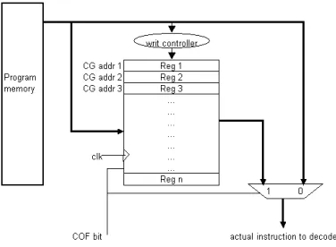
To implement reconfiguration of instructions, introduce a new mechanism called Instruction Re-map buffer (IRB). The IRB can be viewed as a register in the CPU. Each entry in this table can hold a valid uncompressed instruction of size equal to 16 bits, the entry has a unique address which forms the compressed representation. A pair of special instructions is added to the existing instruction set to allow reconfiguration of the IRB. Once an instruction is written into the IRB, it can be referenced by the address of its location. Since the width of the address, which is the compressed instruction, is smaller than that of the actual instruction, we achieve com pression.
Figure 1. Instruction re-map buffer.
A. Design Of Instruction re-map buffer
The instructions to be compressed are first written into locations Loc1 to LocN in the instruction re-map buffer as shown in Fig. 1. Configuring the re-map buffer will be discussed in Section 4.3. After configuring the IRB, each of the locations in it holds a 16-bit instruction. The width of the address of these locations is equal to log2N where N is the number of locations in the instruction re-map buffer. Addr1 in the figure is the address of first location (Loc1 ), Addr2 is the address of second location (Loc2 ), and so on. Each instruction that is written into the table can now be referenced by the address of its corresponding location. Now, the instructions that are written into the instruction re-map buffer have a unique compressed representation. All these instructions in the program memory are now replaced by their compressed representation.
Decompression of the compressed instruction is achieved as follows. The re-map buffer instructions are stored with cyclic-gray code as shown in Fig. 1. Thus the output of the multiplexer is the uncompressed encoding of the fetched instruction. Note that with the above compression scheme, instruction widths could become non-standard size. That is, uncompressed instructions are 16-bit wide while each compressed instruction could be 8-bit wide, for a re-map buffer size of 128 locations.
V. IMPLEMENT OF INSTRUCTION RE-MAP BUFFER
(An ISO 3297: 2007 Certified Organization)
Vol. 4, Issue 2, February 2015
Now, the instructions that are written into the instruction re-map buffer have a unique compressed representation. All these instructions in the program memory are now replaced by their compressed representation .
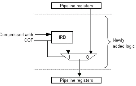
Then it is executed in the Execute stage and the results are stored in write back stage of the pipeline. We enhance the DSP core with the inclusion of the Instruction re-map buffer . The instruction re-map buffer fits in the pre-decode stage of the pipeline as indicated in Fig. 2.
Figure 2. Modified decoded stage
These instruction re-map buffer tables accessing same as general-purpose register in the existing chip. The time of access time bottlenecks are very small is equivalent to the SRAM module time and fits in the predecode stage
VI. CONFIGURING THE REGISTER-PROGRAM TABLE
In this section we discuss how to configure the IRB. We introduced three instruction COFST, COFED and COFRE. The first pair instruction is used for to copy program instruction in to the IRB register.
COFST <address>: This instruction is decoded by the configuration controller in the IRB and a CALL instruction is passed on to the instruction decoder. In addition, a COF bit and configuration in the re-map buffer is set This instruction is decoded by the instruction decoder, the CPU control unit copy the instructions from the program memory to instruction re-map buffer until the COFED executing. Due to the COF bit set the all instruction are now flow through IRB and original uncompressed instruction are generated.
COFED: This instruction is decoded by the configuration controller. This instruction resets the configuration bit in the instruction re-map buffer. This turns on the instruction decoder. The configuration controller sends a return instruction to the instruction decoder and the program control transfers back to the calling program and starts executing the instructions.
COFRE: This instruction reset the COF bit, so that the processor works on normal mode.
Figure 2. Cyclic gray code instruction mapping
sequences to exploit the instruction usage in different code segments are inserted in the beginning of each segment of code. In the example shown in Fig. 3, the instruction re-map buffer is configured twice, once for code segment 1 and once for code segment 2.
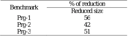
VII. EXPERIMENTAL RESULTS: CODE SIZE REDUCTION
This paper use standard benchmark programs are used to evaluate the improvement in code size. These benchmarks are named Prg1, Prg2 and Prg3. Table 1 represent the percentage reduction in code size for the three benchmarks.
Benchmark % of reduction Reduced size
Prg-1 56
Prg-2 42
Prg-3 51
Table 1. Percentage of code reductions VIII. RE-CONFIGURATION FOR LOW POWER
In this section, the detail the approach to reduce power consumption using re-configurable instructions. In a processor, instruction fetching contributes to a significant portion of the overall power consumption. This power spent depends on the switching activity on the program address bus and that on the program data bus. Our experimental results indicate that program data bus contributes to over 80% of the total number of toggles. Hence focus on reducing the number of toggles on program data bus. The number of toggles on program data bus depends on the choice of encodings for the consecutive instructions in the dynamic sequence and the total number of fetches made. With re-configurable instructions, we reduce both the number of fetches needed and the number of toggles between consecutive fetches of the compressed instructions Firstly, it will reduce the number of bits fetched by compressing a set of most commonly occurring instructions. Further, using Cyclic-Gray codes for encoding the instructions, reduce the number of toggles between consecutive fetches of compressed instructions.
The entire sequence of program is profiled to get instruction usage information. Based on this information, a set of top most commonly used instructions are chosen and are low bit width compressed. Due to this, the number of bits fetched reduces. The compressed instructions, fetched in consecutive accesses, are assigned with Cyclic-Gray coded values to
further reduce the number of toggles.
I1 111
I2 101
I3 100
Loop : I4 000
I5 001
I6 011
End loop I7 010
I8 110
I9 ….
I10 ….
(An ISO 3297: 2007 Certified Organization)
Vol. 4, Issue 2, February 2015
IX. POWER REDUCTION
In a DSP processor, instruction fetching play a part to a significant portion of the overall power consumption. The primary contributor to the instruction fetch power is the toggling of high capacitance nets that connect the CPU and the memory. The voltage change on a gate capacitance requires charge transfer, and therefore causes power consumption. The toggle in program memory data bus is too high hence the power consumption on data bus high.
The toggles in the program address bus are due to the changes in PC values used in fetching the instructions, while the toggles in the program data bus are due to the instructions fetched. The toggles in the program data bus are likely to be higher and contribute significantly to the instruction fetch power. To establish this, we measure the toggles in program address and data buses in three slandered benchmarks is reported in Table 2
Benchmark
Percentage contribution to total number of toggle Program
address bus
Program data bus
Prg-1 22.5 77.5
Prg-2 17.5 82.5
Prg-3 22.6 77.4
Table 2. Toggle distribution on program address and program data buses.
B. Energy Saving
The address and data bus require an amount of current that is proportional to the overall bus-switching rate. Energy measurements are made as follows. We obtain the switching activity information on the CPU program memory interface and on the register-program execution using flips finding program.
As per the Texas Instruments [5] the current consumption per line are calculated by using number of flips per second. Based upon the simulation time the energy is calculated. Energy reduction for pre reconfigured execution for different table sizes are summarized in Table 3
Register Size
Energy spent (Normalized) Prg-1 Prg-2 Prg-3
0 1 1 1
32 0.5 0.63 0.73
64 0.18 0.23 0.31
Table 3. Energy spent in pre-written execution. X. CONCLUSION
The proposed a mechanism instruction re-map buffer which to reduce the power consumption of DSP processor with minimal hardware overhead. The paper explained an incremental redesign of the TMS320c54x CPU to include the instruction re-map buffer. The paper showed that the same hardware mechanism could be used for reduction of code size and target power. The paper presented standard benchmarks program in our analysis. In our evaluations, we have taken into account the overhead due to instruction re-map table timing. This paper showed that code size improvement of over 56% on an optimized code can be achieved and about 82 % instruction fetch energy can be reduced
REFERENCES
2. G. Araujo, P. Centoducatte, M. Cortes, and R. Pannain. Code compression based on operand factorization. International Symposium on Microarchitecture, 1998
3. L. Benini, G. Micheli, E. Macii, D. Sciuto, and C. Silvano, “Asymptotic Zero-Transition Activity Encoding for Address Busses in Low-Power
Microprocessor-Based Systems,’’in Proceedings of the 7th Great Lakes Symposium on VLSI, pp. 77– 82, Urbana-Champaigne, IL, March 1997.
4. L. Benini, F. Menichelli, and M. Olivieri, “A Class of Code Compression Schemes for Reducing Power Consumption in Embedded
Microprocessor Systems,’’ IEEE Trans. Comput., vol. 53, no. 4, 2004, pp. 467–482.
5. Calculation of TMS320LC54x Power Dissipation," 1997, Application report, Texas Instruments.
http://www-s.ti.com/sc/psheets/spra164/spra164.pdf.
6. A. Chandrakasan and R. Brodersen, “Low Power Digital CMOS Design,’’ Kluwer, 1995.
7. S. Debray, W. Evan, R. Muth, and B. de Sutter, “compiler Techniques for Code Compression,’’ ACM Trans. Program. Lang. Syst., 2000, pp.
378–415.
8. L.H. Lee, W. Moyer, and J. Arends, “Instruction Fetch Energy Reduction Using Loop Caches For Embedded Applications with Small Tight
Loops,’’ in Proceedings of International Symposium on Low Power Electronics and Design, pp. 267– 269, San Diego, CA, August 1999.
9. M. Mehendale, S.D. Sherlekar, and G. Venkatesh, Bextensions to Programmable DSP Architectures for Reduced Power Dissipation,’’ in
Proceedings of International Conference on VLSI Design, pp. 37–42, Chennai, India, January 1998.
10. S. Manne, A. Klauser, and D. Grunwald, “Pipeline Gating: Speculation Control for Energy Reduction,’’ in Proceedings of International
Symposium on Computer Architecture, pp. 132–141, Barcelona, Spain, June 1998.
11. J. Rabaey and M. Pedram, “Low Power Design Methodologies,’’ Kluwer Academic. Publishers, 1996.
12. C. Su, C. Tsui, and A. Despain, “Saving Power in the Control Path of Embedded Processors,’’ IEEE Des. Test Comput., vol. 11, 1994, pp. 24–
30
13. M. Stan and W. Burleson, “Bus-Invert Coding for Low Power I/O,’’ IEEE Trans. Very Large Scale Integr. (VLSI) Syst., vol. 3, 1995, pp. 49–
58.
14. Texas Instruments, TMS320C54x DSP CPU and Instruction Set Reference Guide,’’ June
1998.http://acomms.whoi.edu/micromodem/TIDocs/c54x%20Ref%20Vol2%20Mnemonic%20Instr.pdf
15. S.J.E. Wilton and N.P. Jouppi, “CACTI: An Enhanced Cache Access and Cycle Time Model,’’ IEEE J. Solid-State Circuits, vol. 31, no. 5, May
1996, pp. 677–688.
16. A. Wolfe and A. Chanin. Executing Compressed Programs on an Embedded RISC Architecture. In Proc. Int’l Symp. On Microarchitecture,
1992.
17. S. Devadas, S. Liao, and K. Keutzer. Code density optimization for embedded DSP processors using data compression techniques. Adavanced
Research in VLSI, 1995
18. C. Lefurgy, P. Bird, I.-C. Chen, and T. Mudge. Improving Code Density Using Compression Techniques. Technical Report CSE-TR-342-97, 8