Circuit Clustering for Cluster-based
FPGAs Using Novel Multiobjective
Genetic Algorithms
Yuan Wang
Ph.D
University of York
Electronics
September 2015
Abstract
Circuit clustering is one of the most crucial steps in a post-synthesis FPGA CAD flow. It attempts to efficiently fit synthesised logic functions into FPGA logic clusters. On a FPGA, different clusterings result in different circuit mappings, which affect FPGA utilisation, routability and timing, and therefore impact the circuit performance. This research proposes the use of a Multi Objective Genetic Algorithm (MOGA) as a methodology to solve the cluster-based FPGA circuit clustering problem.
Four alternative approaches based on MOGA methods are proposed in this research: RVPack is inspired by the stochastic feature that exists in Evo-lutionary Algorithms (EAs). GGAPack, GGAPack2, DBPack and HYPack, T-HYPack (Timing-driven HYPack) are then proposed and developed, which are fully customised MOGA-based circuit clustering methods. GGAPack clusters a circuit using a top-down perspective, and DBPack uses a new bottom-up perspective. HYPack combines GGAPack and HYPack – a hybrid method. According to experimental results, a few conclusions are drawn: It is possible to improve the performance of the greedy algorithm based circuit clustering methods by incorporating randomness. The performance of MOGA based top-down clustering is poor; however, using MOGA to cluster a circuit from a bottom-up perspective can produce better solutions. T-HYPack clus-tered circuit has the best timing performance compared with state-of-the-art methods. The experimental results also reflect a wider potential for using GAs to solve FPGA circuit mapping problems.
Contents
Abstract 2 Contents 3 List of Tables 11 List of Figures 18 Acknowledgement 37 Declaration 38 1 Introduction 39 1.1 Background . . . 39 1.2 Motivation . . . 43 1.3 Research hypothesis . . . 44 1.3.1 Statement of hypothesis . . . 44 1.3.2 Analysis of hypothesis . . . 451.4 Novel contributions . . . 46
1.5 Thesis structure . . . 48
2 Reconfigurable Devices 51 2.1 Introduction to reconfigurable devices . . . 51
2.2 Field Programmable Gate Array (FPGA) . . . 53
2.2.1 Definition . . . 53
2.2.2 Applications . . . 54
2.2.3 Advantages and disadvantages . . . 55
2.3 Overview of FPGA architectures . . . 57
2.3.1 Basic architecture . . . 57
2.3.2 Programmable logic architecture . . . 58
2.3.3 Routing architecture . . . 62
2.3.4 Heterogeneous block . . . 67
2.4 Cluster-based island-style FPGA and its model . . . 69
2.4.1 CLB and BLE model . . . 70
2.4.2 Routing architecture model . . . 72
2.5 Summary . . . 75
3 CAD for FPGAs and Circuit Clustering Methods 77 3.1 Why Computer-Aided Design (CAD)? . . . 77
3.2 A complete CAD flow for FPGAs . . . 78
3.2.1 Overview CAD flow for FPGAs . . . 78
3.2.2 CAD flows in academic research . . . 85
3.3 Circuit clustering . . . 88
3.3.1 Definition . . . 88
3.3.2 Significances and limitations . . . 89
3.3.3 Requirements of circuit clustering . . . 90
3.3.4 MCNC-20 benchmark . . . 94
3.4 Previous methods . . . 94
3.4.1 Bottom-up methods . . . 95
3.4.2 Top-down methods . . . 103
3.4.3 Other methods . . . 105
3.4.4 Advantages and disadvantages . . . 107
3.5 Summary . . . 108
4 Evolutionary Computing 109 4.1 Evolutionary Computing (EC) . . . 109
4.2 The inspiration of nature . . . 110
4.2.1 The theory of Darwin’s natural selection . . . 110
4.2.2 Basic concepts of evolution . . . 112
4.3.1 Representation . . . 118
4.3.2 Variation . . . 119
4.3.3 Evaluation . . . 123
4.3.4 Selection . . . 125
4.3.5 Termination conditions . . . 127
4.4 The Genetic Algorithm . . . 127
4.4.1 Simple Genetic Algorithm (SGA) . . . 128
4.4.2 Multi-Objective Genetic Algorithm (MOGA, or MOEA)129 4.4.3 Constraint handling in MOGAs . . . 132
4.5 Advantages and disadvantages . . . 133
4.6 Summary . . . 134
5 RVPack: Bottom-Up Circuit Clustering Approach Using A Stochastic Perspective Greedy Algorithm 135 5.1 Introduction . . . 135
5.2 The VPack algorithm in detail . . . 136
5.3 Disadvantages of the VPack algorithm . . . 142
5.4 The Random VPack (RVPack) . . . 145
5.4.1 Motivation . . . 145
5.4.2 Implementation . . . 145
5.6 Experimental results . . . 151
5.6.1 RVPack direct outputs . . . 151
5.6.2 RVPack VPR results . . . 154
5.7 Discussion . . . 157
5.8 Summary . . . 158
6 GGAPack: Top-Down Circuit Clustering Approach Using MOGAs 160 6.1 Introduction . . . 160 6.2 Motivation . . . 161 6.3 GGAPack implementation . . . 162 6.3.1 Representation . . . 163 6.3.2 Reproduction . . . 164 6.3.3 Multiobjective selection . . . 168
6.3.4 Evaluating the evolved designs . . . 171
6.3.5 Summary of GGAPack . . . 173
6.4 Initial experimental results . . . 173
6.4.1 GGAPack experimental setups . . . 173
6.4.2 GGAPack direct outputs . . . 177
6.5.1 Seeding GGAPack with semi-optimal solutions
– GGAPack2 . . . 179
6.5.2 GGAPack2 experimental setups . . . 180
6.5.3 GGAPack2 direct outputs . . . 182
6.5.4 GGAPack2 VPR results . . . 187
6.6 Discussion . . . 191
6.7 Summary . . . 192
7 DBPack: Bottom-Up Circuit Clustering Approach Using MO-GAs 194 7.1 Introduction . . . 194 7.2 Motivation . . . 195 7.3 DBPack implementation . . . 196 7.3.1 Representation . . . 197 7.3.2 Reproduction . . . 198 7.3.3 Multiobjective evaluation . . . 201 7.3.4 Solution selection . . . 205 7.3.5 Summary of DBPack . . . 206 7.4 Experimental setups . . . 208 7.5 Experimental results . . . 211
7.5.2 DBPack VPR results . . . 217
7.6 Discussion . . . 221
7.7 Summary . . . 222
8 HYPack/T-HYPack: Hybrid Circuit Clustering Approach Using MOGAs 224 8.1 Introduction . . . 224
8.2 Motivation . . . 225
8.3 Implementation . . . 226
8.3.1 MOGA based hybrid two-phase circuit clustering – HY-Pack . . . 226
8.3.2 Timing-driven HYPack – T-HYPack . . . 229
8.4 Experimental setups . . . 233
8.5 Experimental results . . . 235
8.5.1 HYPack direct outputs . . . 235
8.5.2 T-HYPack outputs . . . 240
8.6 Discussion . . . 248
8.7 Summary . . . 250
9 Conclusion and Future Work 251 9.1 Key findings . . . 251
9.3 Future work . . . 262
Appendices 265
List of Abbreviations 312
List of Tables
2.1 The configurable levels in digital and analogue configurable devices with different granularities (Trefzer and Tyrrell, 2015) 53
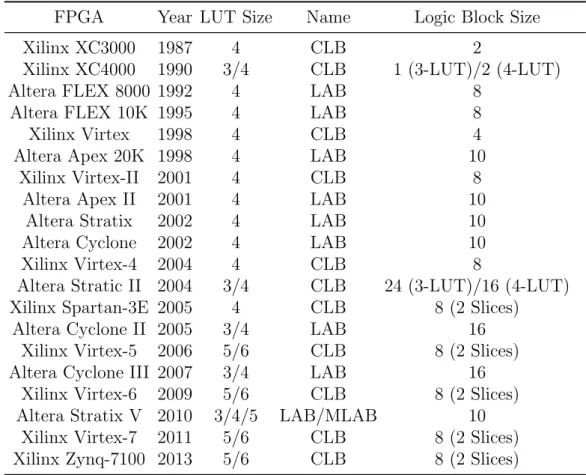
2.2 Mainstream FPGA LUT sizes, larger logic block names, and larger logic block sizes over years . . . 61
2.3 CLB (BLE) model parameters and meanings (Marquardt, 1999) 71
2.4 Routing architecture model parameters and meanings . . . 75
3.1 The comparison of three placement methods (Vygen, 2002) . . 82
3.2 Gains of each connection in Figure 3.7 circuit, gain calculations are based on Equations 3.12 - 3.13 . . . 100
4.1 Binary code of x, and the result of y for finding the minimum value of Equation 4.1. . . 118
5.1 The number of inputs for each BLE . . . 138
5.2 “Gain” values obtained via the cost function . . . 139
5.3 Statistics for average highest gain BLE number of appearances per absorption in the VPack . . . 144
5.4 FPGA model details for evaluating clustered circuits in VPR (Marquardt, 1999) . . . 150
5.5 RVPack execution time comparisons, single execution. Data boxplot and detailed data are provided in Appendices in Figure A.7 and Table A.5. . . 153
5.6 Worst case RVPack on FPGA area usage, X×Y arrays, for MCNC-20 benchmarks compared to VPack, lower is better. Data boxplot and detailed data are provided in Appendices in Figure A.8 and Table A.6. . . 154
6.1 Sums of clustered CLB numbers for the MCNC-20 benchmarks between different algorithms – sorted in ascending order, lower is better. . . 184
6.2 Sums of clustered CLB interconnects for the MCNC-20 bench-marks between different algorithms – sorted in ascending order, lower is better. . . 185
6.3 Single execution time comparisons for GGAPack, GGAPack2, RVPack (average) and VPack . . . 186
6.4 GGAPack2 on FPGA area usage,X×Y arrays, for MCNC-20 benchmarks compared to VPack, RVPack and RPack, lower is better. Data boxplot and detailed data are provided in Appendices in Figure A.18 and Table A.16. . . 188
7.1 Sums of clustered CLB numbers for the MCNC-20 benchmarks between different algorithms – sorted in ascending order, lower is better. . . 212
7.2 Sums of clustered CLB interconnects and improvements com-pared to DBPack best case results for MCNC-20 benchmarks between different algorithms – sorted in ascending order, lower is better. . . 213
7.3 A clustered CLB in benchmark “clma” . . . 215
8.1 Sums of clustered CLB numbers for MCNC-20 benchmarks between different algorithms – sorted in ascending order, lower is better. . . 236
8.2 Sums of clustered CLB interconnects and improvements com-pared to HYPack best case results for MCNC-20 benchmarks between different algorithms – sorted in ascending order, lower is better. . . 238
8.3 Sums of shortest, average and longest execution time for MCNC-20 benchmarks between GGAPack2, DBPack and HY-Pack – sorted in ascending order. . . 239
8.4 Sums of clustered CLB numbers for ten selected MCNC-20 benchmarks between different algorithms – sorted in ascending order, lower is better. . . 241
8.5 Sums of clustered CLB interconnects for ten selected MCNC-20 benchmarks between different algorithms – sorted in ascending order, lower is better. . . 242
8.6 Single execution time comparisons for ten small MCNC-20 benchmarks . . . 243
8.7 T-HYPack, RVPack, T-VPack, DBPack and the VPack on FPGA area usages, X ×Y arrays, for ten small MCNC-20 benchmarks, lower is better. . . 243
8.8 Best timing performed T-HYPack results compared to T-VPack247
9.1 Comprehensive comparisons for proposed methods – RVPack, GGAPack2, DBPack and HYPack via full MCNC-20 bench-marks, figures indicate improvements and higher is better. . . 259
9.2 Comprehensive comparisons for proposed methods – RVPack, GGAPack2, DBPack, HYPack and T-HYPack via 10 selected MCNC-20 benchmarks, figures indicate improvements and higher is better. . . 260
9.3 A general comparison for well-known FPGA circuit clustering methods, figures indicate improvements and higher is better. . 261
A.1 Synthesised MCNC-20 benchmarks . . . 267
A.2 Synthesised MCNC-20 benchmarks after the pattern match . . 268
A.3 Medians of Figure A.5 – boxplot of RVPack clustered CLB number for MCNC-20 benchmarks . . . 278
A.4 Medians of Figure A.6 – boxplot of RVPack clustered CLB interconnect number for MCNC-20 benchmarks . . . 279
A.5 Medians of Figure A.7 – boxplot of RVPack execution time for MCNC-20 benchmarks . . . 280
A.6 Medians of Figure A.8 – boxplot of RVPack on FPGA area usages for MCNC-20 benchmarks . . . 281
A.7 Medians of Figure A.9 – boxplot of RVPack on FPGA channel widths for MCNC-20 benchmarks . . . 282
A.8 Medians of Figure A.10 – boxplot of RVPack on FPGA wire lengths for MCNC-20 benchmarks . . . 283
A.9 Medians of Figure A.11 – boxplot of RVPack on FPGA circuit-critical-path delays for MCNC-20 benchmarks . . . 284
A.10 Medians of Figure A.12 – boxplot of GGAPack clustered CLB number for MCNC-20 benchmarks . . . 285
A.11 Medians of Figure A.13 – boxplot of GGAPack clustered CLB interconnect number for MCNC-20 benchmarks . . . 286
A.12 Medians of Figure A.14 – boxplot of GGAPack execution time for MCNC-20 benchmarks . . . 287
A.13 Medians of Figure A.15 – boxplot of GGAPack2 clustered CLB number for MCNC-20 benchmarks . . . 288
A.14 Medians of Figure A.16 – boxplot of GGAPack2 clustered CLB interconnect number for MCNC-20 benchmarks . . . 289
A.15 Medians of Figure A.17 – boxplot of GGAPack2 execution time for MCNC-20 benchmarks . . . 290
A.16 Medians of Figure A.18 – boxplot of GGAPack2 on FPGA area usages for MCNC-20 benchmarks . . . 291
A.17 Medians of Figure A.19 – boxplot of GGAPack2 on FPGA channel widths for MCNC-20 benchmarks . . . 292
A.18 Medians of Figure A.20 – boxplot of GGAPack2 on FPGA wire lengths for MCNC-20 benchmarks . . . 293
A.19 Medians of Figure A.21 – boxplot of GGAPack2 on FPGA circuit-critical-path delays for MCNC-20 benchmarks . . . 294
A.20 Medians of Figure A.22 – boxplot of DBPack clustered CLB number for MCNC-20 benchmarks . . . 295
A.21 Medians of Figure A.23 – boxplot of DBPack clustered CLB interconnect number for MCNC-20 benchmarks . . . 296
A.22 Medians of Figure A.24 – boxplot of DBPack execution time for MCNC-20 benchmarks . . . 297
A.23 Medians of Figure A.25 – boxplot of DBPack on FPGA area usages for MCNC-20 benchmarks . . . 298
A.24 Medians of Figure A.26 – boxplot of DBPack on FPGA channel widths for MCNC-20 benchmarks . . . 299
A.25 Medians of Figure A.27 – boxplot of DBPack on FPGA wire lengths for MCNC-20 benchmarks . . . 300
A.26 Medians of Figure A.28 – boxplot of DBPack on FPGA circuit-critical-path delays for MCNC-20 benchmarks . . . 301
A.27 Medians of Figure A.29 – boxplot of HYPack clustered CLB number for MCNC-20 benchmarks . . . 302
A.28 Medians of Figure A.30 – boxplot of HYPack clustered CLB interconnect number for MCNC-20 benchmarks . . . 303
A.29 Medians of Figure A.31 – boxplot of HYPack execution time for MCNC-20 benchmarks . . . 304
A.30 Medians of Figure A.32 – boxplot of T-HYPack clustered CLB number for MCNC-20 benchmarks . . . 305
A.31 Medians of Figure A.33 – boxplot of T-HYPack clustered CLB interconnect number for MCNC-20 benchmarks . . . 306
A.32 Medians of Figure A.34 – boxplot of T-HYPack execution time for MCNC-20 benchmarks . . . 307
A.33 Medians of Figure A.35 – boxplot of T-HYPack on FPGA area usages for MCNC-20 benchmarks . . . 308
A.34 Medians of Figure A.36 – boxplot of T-HYPack on FPGA channel widths for MCNC-20 benchmarks . . . 309
A.35 Medians of Figure A.37 – boxplot of T-HYPack on FPGA wire lengths for MCNC-20 benchmarks . . . 310
A.36 Medians of Figure A.38 – boxplot of T-HYPack on FPGA circuit-critical-path delays for MCNC-20 benchmarks . . . 311
List of Figures
2.1 A generic FPGA architecture (Gokhale and Graham, 2005) . . 57
2.2 A generic 4-input Look-Up Table (LUT) . . . 58
2.3 A generic FPGA programmable logic block (Gokhale and Gra-ham, 2005) . . . 59
2.4 Generic programmable logic cluster, it contains a few logic programmable blocks, and internal routing resources. The internal routing resources can be configured to form connections for internal logic blocks. Moving some connections in the cluster can reduce the routing pressure of FPGA higher routing architecture. . . 60
2.5 Routing-purpose switches used for FPGAs (Gokhale and Gra-ham, 2005) . . . 62
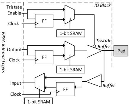
2.6 A generic FPGA programmable input and output block (Gokhale and Graham, 2005) . . . 63
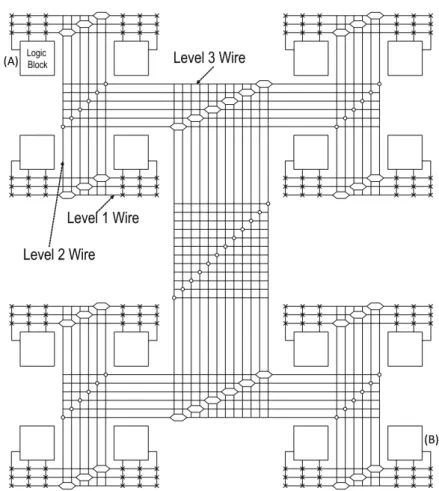
2.7 Hierarchical routing architecture FPGA example, if the upper left corner logic cluster (A) has a signal to the upper right corner logic cluster (B), a routing flow will be as follows: Level 1, Level 2, Level 3, and back to Level 2, Level 1 at the right of the figure. (Tsu et al., 1999) . . . 64
2.8 A generic island-style FPGA routing architecture (Kuon et al., 2007) . . . 66
2.9 Cluster-based FPGA BLE and CLB internal structures (Betz et al., 1999) . . . 70
2.10 Detailed island-style FPGA routing architecture (Betz et al., 1999) . . . 73
2.11 Disjoint and Wilton switch box (Kuon et al., 2007) . . . 74
2.12 The definition of wire segment length, this figure also shows the staggered wire segments. (Marquardt, 1999; Kuon et al., 2007) . . . 74
3.1 A simplified FPGA CAD flow (Betz et al., 1999), it is a sequen-tial process, and contains three steps: Synthesis, placement and routing. . . 79
3.2 Details of synthesis and logic block packing (Betz et al., 1999) 80
3.3 A research based CAD flow for FPGAs (Luu et al., 2011) . . . 85
3.4 An example to show the process of circuit clustering (Mar-quardt, 1999) . . . 89
3.5 Mapping results under different CLB interconnect numbers, when a clustered circuit has fewer CLB interconnects (nets), the routed circuit can have fewer tracks (Marquardt, 1999). Therefore, a narrow channel width is used on the FPGA. . . . 91
3.7 An example circuit for showing connection gains in the RPack, CLB relevant connections, (a), mean these connections share current CLB connections. Independent connections, (b), mean these connections either can be absorbed in the current CLB or not sharing connections to the current CLB. . . 99
3.8 BLE Ahas a larger “c”, in contrast, BLE B has a smaller “c”. For example, a CLB can accommodate 5 BLEs, using smaller “c” BLE as a seed can absorb 4 connections in a CLB; squares represent BLEs. When usesBLE Aas a seed, no matter how to cluster 5 BLEs, the CLB cannot include 4 connections (Singh and Marek-Sadowska, 2002). . . 101
4.1 Why giraffes have long necks, explanation based on the theory of Darwin’s natural selection (Rikizo and Suzuki, 1974). . . 111
4.2 Chromosome and gene of an organism, a cell contains a genome (a few chromosomes) or a single chromosome depending on the type of organism. Genetic information is stored on DNA, and DNA comprises of a long chain of base pairs. A set of base pairs is called a gene, which controls organism’s physical traits. The position of gene is known as locus (GENCODYS, 2010). . 113
4.3 Detailed process of meiosis: A diploid cell contains paternal and maternal chromosomes, or called chromatids (single pair). In the interphase, chromatids are self copied. In the first step of meiosis, chromosomes are aligned and formed as homologous chromosomes – tetrad. The paris of chromatids are joint at random crossing points – chiasmata. In the second step of meiosis, chromatids are first divided into two cells, and further divided into four sets of chromosomes stored in gametes. . . . 114
4.5 Binary string can be used to represent the status of switches in a circuit: (a), binary code can control “on” and “off” of a switch, so input of a circuit is controllable. (b), binary code can also control a set of switches, for example controlling an inverter is connected in a ring oscillator loop or not – referred to a circuit topology, then the frequency of the oscillator is adjustable. . . 119
4.6 An example of the integer representation – multiple-bin packing: Each integer can be used to represent an item. The value of integer helps to explain which bin the integer matched item is packed. As shown in the figure, items “0” and “3” have a value of “0”, these items is packed in bin “0”. . . 120
4.7 Two mutation operations for integer representation: gene swap-ping and gene inversion. Gene swapswap-ping: Any two genes can be swapped on a chromosome. Gene inversion: The order of a segment of genes is inverted and inserted into the original chromosome. . . 121
4.8 Different crossover operations (Langeheine, 2005): There are four common crossover operations, which are single point crossover – two vectors crossover at a random point, two point crossover – two vectors crossover at two random points, uniform crossover – any element of vectors can be crossovered under a probability and arithmetic crossover – two vectors are executed an arithmetic calculation and generated two new vectors. . . . 122
4.9 3-D fitness landscape (Verel, 2015) . . . 124
4.10 A flow of simple genetic algorithm . . . 128
5.1 VPack circuit clustering flow . . . 137
5.3 A CLB contains two BLEs with one connection inside the CLB, where BLE-4 is the first BLE to have the maximum number of inputs (the seed), and BLE-1 is the first BLE to obtain the highest gain. o 1 is the included connection in the CLB. . . . 140 5.4 An example illustrates how the hill-climbing works. There are
N-1 clustered CLBs are on the left, the Nth CLB, CLB-N – present CLB, is on the right. Since the CLB input constraint, zero-gain BLE-Z cannot be fitted in CLB-N, but can be clus-tered inCLB-2 as they have common connections. . . 141 5.5 Average number of possible seed per CLB in the MCNC-20
benchmarks, each bar shows the number of BLEs in each benchmark, and red-coloured part in each bar indicates the average possible seed number for each CLB clustering. . . 143
5.6 CLB-X is the first CLB clustered by VPack, and it is a unique solution. CLB-Y is the first CLB clustered by RVPack, and it is a possible solution. This means that RVPack can produce different clustering solutions. . . 146
5.7 Different clustering solutions are obtained when the zero gain BLE is inserted into different CLBs, for example CLB-2 or
CLB-5 . . . 148 5.8 RVPack executing and testing flow: Each synthesised
MCNC-20 benchmark netlist is processed by RVPack. RVPack pro-duces new netlists to VPR for further testing. The flow is the same as to VPack. . . 149
5.9 RVPack CLB number for MCNC-20 benchmarks compared to VPack, lower is better. Data boxplot and detailed data are provided in Appendices in Figure A.5 and Table A.3. . . 152
5.10 RVPack CLB interconnect number for MCNC-20 benchmarks compared to VPack, lower is better. Data boxplot and detailed data are provided in Appendices in Figure A.6 and Table A.4. 152
5.11 RVPack on FPGA channel width for MCNC-20 benchmarks compared to VPack, lower is better. Data boxplot and detailed data are provided in Appendices in Figure A.9 and Table A.7. 155
5.12 RVPack on FPGA wire length compared to VPack for MCNC-20 benchmarks, lower is better. Data boxplot and detailed data are provided in Appendices in Figure A.10 and Table A.8. 156
5.13 RVPack on FPGA critical path delay compared to VPack for MCNC-20 benchmarks, lower is better. Data boxplot and detailed data are provided in Appendices in Figure A.11 and Table A.9. . . 156
6.1 An example shows the GGAPack chromosome encoding scheme. The length of chromosome is dependent on the number of BLEs, and each gene position is used to describe the BLE index. The value of gene indicates which CLB the gene represented BLE is allocated. . . 163
6.2 Determining the CLBs for performing the crossover operation. (a), the CLBs are determined randomly, and dashed-box genes
indicate that gene represented BLEs are appeared in the se-lected CLBs. (b), these sese-lected CLBs are directly injected in two individuals of each other. . . 165
6.3 Injecting CLBs into each other and eliminating CLBs that contain injected BLEs, this figure continues Figure 6.2 . . . . 166
6.4 After the CLB exchange, a few BLEs are freed from CLBs. Meanwhile, the injected CLBs, referred to CLB internal BLE combinations, have been exchanged. The question mark gene means that the gene does not have a value – matched to freed BLEs. This figure continues Figures 6.2-6.3 . . . 167
6.5 The GGAPack mutation operation randomly eliminates two CLBs. In the figure, the CLBs are the CLB-0 and CLB-6. After the mutation, the BLEs with these two CLBs are freed. These freed CLBs are needed to insert back to existing CLBs, or new CLBs. . . 168
6.6 Crowding distance calculation of an individual. Solid black dots represent the same Pareto front individuals under the objective-1-and-2-fitness space. The crowding distance of individual i
can be calculated by nearest neighbours – individual i−1 and
i+ 1 – the perimeter of a cuboid which is formed by individual
i−1 and i+ 1. . . 170 6.7 The flow of GGAPack: The population is initialised randomly
– each BLE is in a CLB with a random CLB index. Individuals are assigned multiple fitnesses by multiple fitness functions. MO selection uses the non-dominated sort and crowding dis-tance (NSGA-2 method) to form new population. GGAPack, the GA, iterates for a fixed number of generations then stops. The best individual is filtered and translated as a netlist. . . . 174
6.8 GGAPack executing and testing flow. Before forwarding the synthesised MCNC-20 netlist (LUTs + FFs) to GGAPack, a duplicated process, the pattern match, can be first performed, so that the GGAPack deals with the BLEs directly. . . 175
6.9 Box plot of CLB numbers vs. different crossover rates of GGAPack executions. The test is based on “clma” – the largest benchmark in MCNC-20. For each crossover rate, GGAPack executes for 100 times, final CLB number means that each GGAPack executes for 40,000 generations. When the crossover rate is 0.6, the GA result variation is small, and CLB number is small as well. . . 176
6.10 GGAPack clustered CLB number for MCNC-20 benchmarks compared to VPack and RVPack, lower is better. Data boxplot and detailed data are provided in Appendices in Figure A.12 and Table A.10. . . 177
6.11 GGAPack clustered CLB interconnect for MCNC-20 bench-marks compared to VPack and RVPack, lower is better. Data boxplot and detailed data are provided in Appendices in Figure A.13 and Table A.11. . . 178
6.12 GGAPack2 working flow: A new mechanism has be added in GGAPack2 which allows it to read clustered solutions that are produced by other circuit clustering algorithms. This mecha-nism reads the solutions and translates them as chromosomes for GGAPack individuals. . . 180
6.13 GGAPack2 executing and testing flow: Similar to GGAPack, each synthesised and pattern matched MCNC-20 benchmark netlist is processed by GGAPack2. GGAPack2 then produces new netlists to VPR for further testing. . . 181
6.14 GGAPack2 clustered CLB number compared to GGAPack, VPack, RVPack and RPack for MCNC-20 benchmarks, lower is better. Data boxplot and detailed data are provided in Appendices in Figure A.15 and Table A.13. . . 183
6.15 GGAPack2 clustered CLB CLB interconnect number compared to GGAPack, VPack, RVPack and RPack for MCNC-20 bench-marks, lower is better. Data boxplot and detailed data are provided in Appendices in Figure A.16 and Table A.14. . . 184
6.16 Shortest execution time compared to GGAPack and GGAPack2 for MCNC-20 benchmarks, lower is better. Data boxplot and detailed data are provided in Appendices in Figures A.14, A.17 and Tables A.12, A.15. . . 185
6.17 GGAPack2 on FPGA channel width compared to RVPack and VPack for MCNC-20 benchmarks, lower is better. Data boxplot and detailed data are provided in Appendices in Figure A.19 and Table A.17. . . 189
6.18 GGAPack2 on FPGA wire length compared to RVPack and VPack for MCNC-20 benchmarks, lower is better. Data boxplot and detailed data are provided in Appendices in Figure A.20 and Table A.18. . . 189
6.19 GGAPack2 on FPGA critical path delay compared to RVPack and VPack for MCNC-20 benchmarks, lower is better. Data boxplot and detailed data are provided in Appendices in Figure A.21 and Table A.19. . . 190
7.1 DBPack chromosome for 12-BLE circuit clustering problem: In the chromosome, the position of gene is used to encode the BLE index, and the gene value indicates the selectivity of corresponding BLE, where “1” means selecting the BLE, “0” indicates a non-selected BLE. . . 198
7.2 The remaining BLE indexes are based on the longest chromo-some. If some BLEs are used to build a CLB, these BLE’s genes are removed from the chromosome. Next GA chromo-some is based on the remaining (unclustered) BLEs, but their indexes still use the longest chromosome. . . 198
7.3 DBPack GA crossover operation. This crossover operation cre-ates two offspring. The crossover point is determined randomly. Then original individuals are crossovered to generate offspring 199
7.4 DBPack GA mutation operation. The mutation operation is the classic “flipping a bit ” mutation, and it occurs to one crossovered offspring. Each mutation operation flips one gene, and only one gene. . . 199
7.5 Box plot of generations vs. different mutation rates when finding a optimal solution. For each mutation rate, GA executes 100 times. M01: mutation rate 0.01%, M02: mutation rate 0.02% to M15: mutation rate 0.15%. M16 is one gene, and only one gene mutation operation. . . 200
7.6 The flow of DBPack solution selection process. All 1st Pareto
front individuals in the GA’s final generation indicate possible solutions for a CLB. If the selection process cannot find the suitable solution where n =N; a solution that has n BLEs, it will perform n−1 and try the process again, until it finds the useful solution. . . 206
7.7 DBPack circuit clustering flow. GA evolution is similar to GGAPack. The major difference is that the DBPack uses a number of discrete GAs to deal with CLB constructions. Once all BLEs have been clustered in CLBs, DBPack will translate all CLBs as a netlist. This netlist can be tested using VPR. . 207
7.8 DBPack executing and testing flow: before forwarding the synthesised MCNC-20 netlist (LUTs + FFs) to DBPack, the duplicated process – the pattern match, is first performed, so the DBPack deals with synthesised BLEs directly. As these programs are executed on a 128-CPU computing cluster, there are maximum 128 DBPack and VPR programs can be executed simultaneously. . . 208
7.9 Box plot of generation numbers (when BLE number is 8) vs. different crossover rates of DBPack executions – clustering first CLB. The test is based on “clma” – the largest benchmark in MCNC-20. For each crossover rate, DBPack first GA executes for 100 times, and stops at when found BLE number is 8 (a CLB can contain 8 BLEs). When the crossover rate is 0.6, the GA generation numbers and variations are small when a solution has 8 BLEs. . . 210
7.10 DBPack clustered CLB number for MCNC-20 benchmarks compared to VPack, RVPack, GGAPack2, RPack, T-VPack and iRAC, lower is better. Data boxplot and detailed data are provided in Appendices in Figure A.22 and Table A.20. . . 211
7.11 DBPack clustered CLB interconnect number for MCNC-20 benchmarks compared to VPack, RVPack, GGAPack2, RPack, T-VPack and iRAC, lower is better. Data boxplot and detailed data are provided in Appendices in Figure A.23 and Table A.21.213
7.12 DBPack shortest execution time compares to GGAPack2. Data boxplot and detailed data are provided in Appendices in Figure A.24 and Table A.22. . . 214
7.13 2-D fitness plots for objectives at the GA last generation, when clustering a CLB in benchmark “clma”. Generation number is 15,000 – maximum. The black dot is the selected individual – the determined CLB. . . 216
7.14 DBPack on FPGA channel width for MCNC-20 benchmarks compared to T-VPack RVPack and VPack, lower is better. Data boxplot and detailed data are provided in Appendices in Figure A.26 and Table A.24. . . 218
7.15 DBPack on FPGA wire length for MCNC-20 benchmarks compared to T-VPack RVPack and VPack, lower is better. Data boxplot and detailed data are provided in Appendices in Figure A.27 and Table A.25. . . 219
7.16 DBPack on FPGA circuit-critical-path delay for MCNC-20 benchmarks compared to T-VPack RVPack and VPack, lower is better. Data boxplot and detailed data are provided in Appendices in Figure A.28 and Table A.26. . . 220
8.1 HYPack working flow. In phase one, DBPack executes for many times to generate enough stochastic clustering solutions. In phase two, these results are selected and used the GGAPack to further optimise the solution. The free BLE reinsertion process in the GGAPack is replaced and uses the DBPack method, where freed BLEs are represented as a DBPack chromosome, and apply DBPack genetic genetic operations to cluster these BLEs as CLBs. . . 227
8.2 An individual after GGAPack crossover operation, some BLEs are freed during this process. Detailed GGAPack crossover operation is introduced in Section 6.3.2. The gene with “?” means the genes represented by this BLEs does not belong to any CLBs. . . 228
8.3 An individual after both crossover and mutation operations, where the mutation is designed to randomly eliminate two CLBs. These CLBs are CLB-2 and CLB-4. Note that this figure is based on the Figure 8.2. After these two operations, freed BLEs are reserved in this individual, and waiting for the BLE reinsertion process to cluster them into CLBs. . . 228
8.4 Each individual, freed BLEs are reinserted by DBPack method. According to the index of the freed BLEs, a new chromosome is created for DBPack. This chromosome is the longest chro-mosome, and BLE indexes are based on this chromosome when performing the DBPack to cluster them. . . 229
8.5 T-HYPack involves VPR for evaluating a solution. After the genetic operation and the reinsertion processes, an individual is converted and assigned fitnesses as in HYPack. At the same time, the individual is exported as a netlist to VPR. VPR then is executed, and its outputs are extracted and represented as new fitnesses for this individual. All fitnesses are used in T-HYPack MO selection. . . 231
8.6 HYPack, T-HYPack executing and testing flow . . . 233
8.7 HYPack clustered CLB number for MCNC-20 benchmarks compared to VPack, RVPack, GGAPack2, RPack, T-VPack, DBPack and iRAC, lower is better. Data boxplot and detailed data are provided in Appendices in Figure A.29 and Table A.27.236
8.8 HYPack clustered CLB interconnects for MCNC-20 bench-marks compared to VPack, RVPack, GGAPack2, RPack, T-VPack, DBPack and iRAC, lower is better. Data boxplot and detailed data are provided in Appendices in Figure A.30 and Table A.28. . . 237
8.9 The shortest execution time comparison between GGAPack2, DBPack and HYPack for MCNC-20 benchmarks, lower is bet-ter. Data boxplot and detailed data are provided in Appendices in Figure A.31 and Table A.29. . . 239
8.10 T-HYPack clustered CLB number for selected ten MCNC-20 benchmarks compared to HYPack, VPack, RVPack, GGA-Pack2, RPack, T-VPack, DBPack and iRAC. lower is better. Data boxplot and detailed data are provided in Appendices in Figure A.32 and Table A.30. . . 240
8.11 T-HYPack clustered CLB interconnect number for selected ten MCNC-20 benchmarks compared to HYPack, VPack, RV-Pack, GGAPack2, RRV-Pack, T-VRV-Pack, DBPack and iRAC. lower is better. Data boxplot and detailed data are provided in Appendices in Figure A.33 and Table A.31. . . 241
8.12 T-HYPack on FPGA channel widths for ten small MCNC-20 benchmarks compared to DBPack, T-VPack, RVPack and VPack, lower is better. Data boxplot and detailed data are provided in Appendices in Figure A.36 and Table A.34. . . 244
8.13 T-HYPack on FPGA wire lengths for ten small MCNC-20 benchmarks compared to DBPack, T-VPack, RVPack and VPack, lower is better. Data boxplot and detailed data are provided in Appendices in Figure A.37 and Table A.35. . . 245
8.14 T-HYPack on FPGA circuit-critical-path delay for ten small MCNC-20 benchmarks compared to DBPack, T-VPack, RV-Pack and VRV-Pack, lower is better. Data boxplot and detailed data are provided in Appendices in Figure A.38 and Table A.36.246
8.15 Different routings of “tseng” benchmark when using VPack and T-HYPack circuit clustering methods. Routing VPack clustered “tseng” circuit on FPGA uses up to 28 tracks in the routing channel. Routing T-HYPack clustered “tseng” circuit on FPGA uses up to 20 tracks in the routing channel. . . 248
A.1 An example of the heterogeneous FPGA structure (Farooq et al., 2011) . . . 266
A.2 GGAPack GA convergence under different evolution time – CLB numbers vs. GA generations. Gen. is short for generation number. The benchmark is “clma” – the largest benchmark in MCNC-20. Test shows that a large generation number is not able to further improve result quality. Short GA stops at 40,000 generations, long (large) GA stops at 60,000 generations. Since 25,000th generation, there is no change in the results in
both GAs. . . 275
A.3 GGAPack GA convergence under different population sizes – CLB numbers vs. GA generations. Pop. is short for population size. The benchmark is “clma” – the largest benchmark in MCNC-20. There is no huge difference, maximum is 2% - 3% in CLB numbers, when the population size is large, but a large population size can significantly slow down a GA execution time - a generation execution time is equal to individual evolution time by population size - when the population size is 100, entire GA execution time will be at least 10 times (1,000%) than the one that has population size 10. . . 276
A.4 DBPack GA convergence – BLE numbers (smallest BLE num-ber among entire population) vs. GA generations when clus-tering the first CLB for benchmark “clma” – the largest bench-mark in MCNC-20. There are two curves: The “Actual” curve shows the smallest BLE number found in GA population – one or a few individuals have this feature. Note that, in order to reduce the clustered CLB number for a clustered circuit, the BLE number is required to match or close to the CLB’s BLE number, which is 8 (one CLB contains, N = 8, 8 BLEs) in this DBPack test. The other curve “Best” (best to a CLB) shows when individual has BLE number as 8 – this indicates the required BLE number individual (solution) is found. When generation number is equal to around 500, “BLE=8” solutions are appeared. Larger generation number designs to fully evolve individuals, where more Pareto optimal solutions can be selected.277
A.5 Boxplot of RVPack clustered CLB number for MCNC-20 bench-marks . . . 278
A.6 Boxplot of RVPack clustered CLB interconnect number for MCNC-20 benchmarks . . . 279
A.7 Boxplot of RVPack execution time for MCNC-20 benchmarks 280
A.8 Boxplot of RVPack on FPGA area usages for MCNC-20 bench-marks . . . 281
A.9 Boxplot of RVPack on FPGA channel widths for MCNC-20 benchmarks . . . 282
A.10 Boxplot of RVPack on FPGA wire lengths for MCNC-20 bench-marks . . . 283
A.11 Boxplot of RVPack on FPGA circuit-critical-path delays for MCNC-20 benchmarks . . . 284
A.12 Boxplot of GGAPack clustered CLB number for MCNC-20 benchmarks . . . 285
A.13 Boxplot of GGAPack clustered CLB interconnect number for MCNC-20 benchmarks . . . 286
A.14 Boxplot of GGAPack execution time for MCNC-20 benchmarks287
A.15 Boxplot of GGAPack2 clustered CLB number for MCNC-20 benchmarks . . . 288
A.16 Boxplot of GGAPack2 clustered CLB interconnect number for MCNC-20 benchmarks . . . 289
A.17 Boxplot of GGAPack2 execution time for MCNC-20 benchmarks290
A.18 Boxplot of GGAPack2 on FPGA area usages for MCNC-20 benchmarks . . . 291
A.19 Boxplot of GGAPack2 on FPGA channel widths for MCNC-20 benchmarks . . . 292
A.20 Boxplot of GGAPack2 on FPGA wire lengths for MCNC-20 benchmarks . . . 293
A.21 Boxplot of GGAPack2 on FPGA circuit-critical-path delays for MCNC-20 benchmarks . . . 294
A.22 Boxplot of DBPack clustered CLB number for MCNC-20 bench-marks . . . 295
A.23 Boxplot of DBPack clustered CLB interconnect number for MCNC-20 benchmarks . . . 296
A.25 Boxplot of DBPack on FPGA area usages for MCNC-20 bench-marks . . . 298
A.26 Boxplot of DBPack on FPGA channel widths for MCNC-20 benchmarks . . . 299
A.27 Boxplot of DBPack on FPGA wire lengths for MCNC-20 bench-marks . . . 300
A.28 Boxplot of DBPack on FPGA circuit-critical-path delays for MCNC-20 benchmarks . . . 301
A.29 Boxplot of HYPack clustered CLB number for MCNC-20 bench-marks . . . 302
A.30 Boxplot of HYPack clustered CLB interconnect number for MCNC-20 benchmarks . . . 303
A.31 Boxplot of HYPack execution time for MCNC-20 benchmarks 304
A.32 Boxplot of T-HYPack clustered CLB number for MCNC-20 benchmarks . . . 305
A.33 Boxplot of T-HYPack clustered CLB interconnect number for MCNC-20 benchmarks . . . 306
A.34 Boxplot of T-HYPack execution time for MCNC-20 benchmarks307
A.35 Boxplot of T-HYPack on FPGA area usages for MCNC-20 benchmarks . . . 308
A.36 Boxplot of T-HYPack on FPGA channel widths for MCNC-20 benchmarks . . . 309
A.37 Boxplot of T-HYPack on FPGA wire lengths for MCNC-20 benchmarks . . . 310
A.38 Boxplot of T-HYPack on FPGA circuit-critical-path delays for MCNC-20 benchmarks . . . 311
Acknowledgement
I would like to first thank the EPSRC (Engineering and Physical Sciences Research Council, UK) for support in funding this research. I would like also thank to my supervisors and group members, Prof. Andy Tyrrell, Dr. James Alfred Walker, Dr. Martin Albrecht Trefzer and Dr. Simon Bale for their guidance and support throughout my Ph.D journey.
A special thanks should also go to my parents for their love and support; without them I would not have been able to come to the UK to receive a higher-standard education. I also need to thank my girlfriend, Miss Zhen Qiu, for three years of her love and patience.
There are a number of other people I would like to thank: Mr. Yunfeng Ma – for spending a lot of time discussing algorithm-related questions. Mr. Jianxin Zhao – my undergraduate supervisor, who always encourages me when I run into trouble. Mrs. Emily Gaspar-Philpott, who has helped with thesis editing and formatting.
Finally, I would like to give my special thanks to Mr. Yunfeng Ma and Yunfeng’s wife, Miss. Xiaoyuan Chen - thanks to them for taking great care of our rented property. Mr. Jingbo Gao - thanks for the times we have worked together in the university library, finishing our thesis writings.
Declaration
I, Yuan Wang, declare that this thesis is a presentation of original work and I am the sole author. This work has not previously been presented for an award at this, or any other, University. All sources are acknowledged as References. My research is part of PAnDA (Programmable Analog and Digital Array) project, and it is funded by the EPSRC. Some (partial) methods and results of this thesis, in collaboration with other authors, are published in the following papers:
Methods and partial results of DBPack (Chapter 7) have been published in the following paper:
• Y. Wang, S. J. Bale, J. A. Walker, M. A. Trefzer, and A. M. Tyrrell, “Multiobjective Genetic Algorithm for Routability-Driven Circuit Clus-tering on FPGAs”, in Proceeding, SSCI2014. IEEE, 2014, pp. 109-116
Methods and partial results of HYPack (Chapter 8) have been published in the following paper:
• Y. Wang, J. A. Walker, S. J. Bale, M. A. Trefzer, and A. M. Tyrrell, “Two-Phase Multiobjective Genetic Algorithm for Constrained Circuit
Chapter 1
Introduction
1.1
Background
Modern electronics can be dated back to the innovation of solid transistors (Edgar, 1930), and the Integrated Circuit (IC) (Jacobi, 1952). In earlier times, electronic systems were built on discrete transistors. Although these transistors have a reduced size and lower power consumption compared with valves (Fleming, 1905), the relatively large size, high power consumption, and the discrete characteristic distribution of transistors are still issues when implementing complex electronic systems. The IC first appeared in 1949 (patent was published on 15 May 1952) where an integrated-circuit-like amplifying device was successfully developed and implemented (Jacobi, 1952). Since IC, the device size, power consumption are gradually decreased, and the component coherence issues are progressively solved. IC allows a number of components; this including transistors, resistors or even capacitors and inductors, implemented on a single silicon chip, which produce a circuit that is powerful, stable, efficient and portable.
Application-Specific Integrated Circuits (ASICs) have become more popu-lar since the IC was born – for instance, the 7400 series digital ICs (Lancaster,
1974). Though an IC can replace a number of discrete transistors or a block of circuits, the IC integration level, in early times, is still low. The industry cannot be satisfied with these still-small-scale ICs, and it continues to be developed. Very-Large-Scale Integrated (VLSI) circuits were invented in the 1970s (Mead and Conway, 1978); today, a very-large-scale IC can contain billions of components. Rather than implementing a simple application, for example an amplifier or a logic gate, these ICs enable the possibility to im-plement higher performance applications, such as a Central Processing Unit (CPU), Digital Signal Processor (DSP), mixed-signal system, and ultimately producing an entire electronic system on a single silicon chip, which is known as SoC (System on a Chip).
With the rapidly increasing needs of complex electronic designs, the flexibility of application-oriented ICs is extremely limited, and the weaknesses of these ICs are exposed. These include the time consuming design cycles, high fabrication and testing costs. In addition, there are also requirements in testing and research, which need fully customised devices. Obviously, application-oriented ICs are not able to meet these requirements. In this case, reconfigurable devices were proposed. These devices are stand-alone ICs, but integrate a number of reconfigurable resources which allow a designer to further configure these ICs on the circuit level so different functions can be realised. Since these reconfigurable ICs can be easily configured, it means that when producing a design using this type of ICs, it largely decreases the design-to-market time, and reduces the engineering costs at the microelectronic level.
FPGA, short for Field Programmable Gate Array, is an important digital reconfigurable device, usually based on Look-Up Tables (LUTs – normally a LUT is composed of a set of Static Random Access Memory cells– SRAMs) and programmable Flip-Flops (FFs), after PLD (Programmable Logic Device, it contains a “fixed-OR, programmable-AND” plane plus memory, the plane can be used to implement “sum-of-products” binary logic equations. If a device does not have the memory, it refers to PLATM–Programmable Logic
Array.) and CPLD (Complex Programmable Logic Device, it might contain many PLAs or PLDs that are linked by programmable interconnections on a single CPLD), and it was initially launched on the market by Xilinx in 1985. FPGAs were then quickly adapted into the electronic industry. Currently, FPGA is a common device to be utilised in for example high performance computing, signal processing, and communication, load-adaptive and fault-tolerant systems. To get a FPGA properly configured, a Computer Aided Design (CAD) flow is used. This flow contains a few key steps, which are circuit synthesis, circuit clustering, clustered circuit placement and routing. By using this flow, it allows a higher level abstraction design to be automatically processed and mapped onto targeted FPGAs.
Circuit synthesis – a HDL (Hardware Design Language) described circuit is automatically synthesised into logic gates (functions).
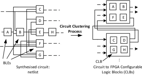
Circuit clustering – as modern FPGAs use logic clusters in their archi-tectures, where a logic cluster is a larger logic macro containing a set of reconfigurable elements that can realise logic functions, synthesised logic gates (functions) have to be grouped, also referred to separate the synthesised circuit, into logic clusters to match a FPGA architecture, at meantime producing less clusters (groups) and cluster interconnects – circuit connections between logic clusters, where such clustered circuit uses less FPGA resources.
Placement – clustered logic clusters are placed onto a FPGA.
Routing – FPGA pre-defined routing resources are used to form connections between the logic clusters in order to form a complete circuit.
Circuit clustering is the first step in post-synthesis processes in FPGA CAD flow. Hence, the quality of a clustered circuit can significantly affect the circuit mapping on a FPGA. If a circuit is poorly clustered, the following CAD processes could not efficiently adjust the circuit and would result in the mapped circuit having low routability, low speed and high power consumption
on the FPGA. On the other hand, circuit clustering usually involves different clustering metrics and also has a number of constraints. As a result, circuit clustering is always an important and difficult process, and it is also the reason that circuit clustering is a hot topic in the area of academic research.
In the early stages, circuit clustering is facilitated by a number of greedy algorithms (Betz and Rose, 1997a; Marquardt et al., 1999; E.Bozorgzadeh et al., 2001; Singh and Marek-Sadowska, 2002; Cormen et al., 2009). They are simple and use a bottom-up clustering perspective, where they cluster a circuit from a local-optimal perspective. When attempts to find a global optimal solution of a problem, dealing with the problem from a local optimal perspective is normally difficult to get the global optimality. Therefore, using the bottom-up methods, the clustered circuit is often less optimal (Feng, 2012). At the same time, clustering metrics are also considered in these algorithms, which use a weighted approach. Although this weighted method can deal with multiple clustering objectives, a better trade off solution is usually difficult to find (Rajavel and Akoglu, 2011). Recently, it has been helpful to use the graph-partitioning-based methods in FPGA circuit clustering methods (Marrakchi et al., 2005; Feng, 2012; Feng et al., 2014a). The graph-partitioning-based methods can cluster a circuit from a global perspective – this is known as top-down clustering methods. These methods are considered to produce better solutions than the greedy algorithms since it uses the global clustering perspective. However, the graph-partitioning-based method mainly focuses on minimising circuit interconnects of partitioned circuits, where it might be difficult to control, for example, which connection is inside a logic cluster, or how many logic functions are in a logic cluster. This means that these types of methods cannot efficiently incorporate clustering metrics and constraints (Marrakchi et al., 2005; Feng, 2012).
1.2
Motivation
Charles Darwin indicated that the root of a large number of different species on the planet was based on the principle of mutation and natural selection, also called natural evolution, and this is the famous theory of Darwin’s natural selection (Darwin, 1859). Darwin considers individuals that are best adapted to an environment can survive, and have chances to produce offspring. In contrast, the less adapted individuals gradually die off, and these individuals are replaced by better individuals. Darwin called this mechanism ”survival of the fittest”.
Genetic Algorithms (GAs) are a subset, or one dialect to be more precise, of Evolutionary Algorithms (EAs), and EAs are the algorithms that imitate the process of natural evolution, and use the natural evolutionary process as a model to solve actual problems (Holland, 1975). GAs are popular in a wide range of areas such as music generation, strategy planning, VLSI technology and machine learning. When a GA is utilised to solve a problem, it is normally not necessary to have specific knowledge about the target problem, which indicates that GAs, or EAs in general, are a model-free heuristic algorithm, and it is an automatic problem solver (Langeheine, 2005). The evolved solutions of a GA are usually useful as proved in the “no free lunch” theorem – “any two optimisation algorithms are equivalent when their performance is averaged across all possible problems” (Wolpert and Macready, 1997). GAs can be extended for supporting multiobjective problems, and this is different from the weighting approach which weights all objectives in a single function to score a solution. In Multi Objective GAs (MOGAs), the multiobjective mechanism is often based on Pareto optimality (Pareto, 1906). This means that MOGA can produce trade off solutions for multiobjective problems (Fonseca and Fleming, 1993).
Research-based FPGA circuit clustering methods have been developed for almost two decades since VPack (Betz and Rose, 1997a). It is notable that there are superior methods, for example T-VPack (Marquardt et al.,
1999) and iRAC (Singh and Marek-Sadowska, 2002). However, these are all bottom-up and greedy-algorithm-based methods, where these algorithms are limited by their “models” and the bottom-up clustering perspective (Singh and Marek-Sadowska, 2002). This implies that these “models” and the clustering perspective can be further enhanced, so the solutions produced by these methods can be improved. PPack (Feng, 2012; Feng et al., 2014a) is a new clustering method based on graph-partitioning methods and uses a top-down clustering perspective. PPack tests show that it can produce excellent circuit clustering solutions compared with previous greedy-algorithm-based methods, but unfortunately PPack cannot efficiently deal with complex clustering objectives and constraints.
As previously introduced, GAs are a model-free and automatic problem solver, and can also be applied to multiobjective problems, where the multiob-jective features can efficiently incorporate targeted obmultiob-jectives of a problem and also problem constraints. Therefore, MOGA can be used to solve the FPGA circuit clustering problem. Using different MOGA designs, the MOGA can either solve the clustering problem from a global perspective, referred as the top-down clustering method, or a local-optimal perspective, the bottom-up clustering method.
1.3
Research hypothesis
1.3.1
Statement of hypothesis
The research hypothesis is as follows:The quality and performance of a multiobjective circuit mapped to a cluster based FPGA can be improved through the use of evolutionary algorithms during the circuit clustering stage of a FPGA computer aided design flow.
1.3.2
Analysis of hypothesis
Nowadays, FPGAs tend to group a number of basic logic blocks, a basic logic block can be as simple as one LUT plus one configurable FF, as logic clusters (Altera Corp., 2001, 2003b,a; Xilinx Inc., 1998, 2010, 2013, 2012b, 2014). This design can reduce the use of reconfigurable resources, and speed up a mapped circuit compared with designs that do not use logic clusters. From the FPGA chip implementation perspective, logic clusters are defined as a large identical logic macro, thus, a FPGA design can be implemented by simply repeating the placement of the macro. From the CAD perspective, when preferentially arranging circuits in logic clusters, it can reduce the difficulties in routing a circuit on a FPGA, as some connections can be formed within logic clusters.
Circuit clustering is a key step in a FPGA CAD flow, where a large synthesised circuit is separated into sub circuits. It has to guarantee that each sub circuit can be mapped onto a FPGA logic cluster, where each sub circuit meets the hardware constraints of the logic cluster. To increase the quality of a clustered circuit, a circuit clustering method is required to cluster more circuit connections in logic clusters, so it can therefore use fewer logic cluster interconnects. In this case, the final routing stage has fewer connections to route. At the same time, the clustering method has to maximise the usage within a logic cluster so fewer logic clusters can be used, which allows more logic to be mapped onto a FPGA. Clustered CLB number and CLB interconnect number can be considered as the routability of a clustered circuit.
Apart from the routability, a circuit clustering method is also required to optimise the performance of clustered circuits. Circuit speed, or timing, is a key factor that affects the performance of a clustered circuit. A circuit speed can be determined by the circuit’s critical path delay. The more stages found in the critical path of a circuit, the lower the circuit speed will be, and the performance of the circuit will be decreased. An effective clustering method usually clusters more critical connections inside FPGA logic clusters, as the FPGA logic cluster has shorter wires and delays, while in the meantime
leaving equally critical or non-critical connections as FPGA logic cluster interconnects. When routing such circuits, circuit speed can be improved.
Genetic algorithms are one subset of evolutionary algorithms – the powerful model-free problem solvers, and can adapt different representations, genetic operations and selection mechanisms, which means genetic algorithms are effective for solving or optimising complex engineering problems. On the other hand, the selection mechanism can be extended to support multiobjective problems. This implies multiobjective genetic algorithms can be a suitable method for exploring the approach of solving the FPGA circuit clustering problem.
1.4
Novel contributions
This doctoral research focuses upon using MOGAs to solve the FPGA circuit clustering problem in a FPGA CAD flow. To achieve this target, a stochastic mechanism is first incorporated into a standard greedy-algorithm-based circuit clustering method. Subsequently, a set of fully customised MOGAs are developed, which represent complete program frameworks for using MOGAs to solve the FPGA circuit clustering problem, and also highlight which clustering perspective (top-down/bottom-up) is efficient for solving this problem. It is also shown which objectives are more effective at optimising the quality of a clustered circuit. In addition, this research also propose an on-line optimisation method to optimise the performance of clustered circuits. This thesis presents four major methods, which are listed as follows:
1) RVPack, short for Random VPack, FPGA circuit clustering method is proposed. This method is based on VPack (Betz and Rose, 1997a). Similar to a GA, which uses stochastic variations to drive evolutions, randomnesses are injected to the greedy-algorithm-based VPack algo-rithm. Although, in this case, RVPack might produce less optimised solutions, some superior solutions can be identified. This method and
its experiments indicate that it is possible to improve solution qualities by incorporating stochastic variations in classic-greedy-algorithm-based circuit-clustering methods.
2) GGAPack/GGAPack2, where GGAPack is short for Grouping Genetic Algorithm Pack, are fully customised and MOGA based FPGA circuit clustering methods. These methods cluster a circuit from a global perspective. Unfortunately, experimental results show that GGAPack is inefficient at producing highly optimised solutions. However, GGA-Pack provides a useful GA framework to solve the circuit clustering problem. GGAPack2 is based on GGAPack – the only difference is that GGAPack2 produces solutions based on RVPack solutions in stead of randomly initialise a population. Real mapping tests show that GGAPack2 solutions are not able to optimise circuit performances, but GGAPack2 can produce better solutions in terms of basic circuit clustering requirements. This means that it might be inefficient to use GAs to solve the FPGA circuit clustering problem from a global perspective.
3) DBPack, short for DataBase Pack, redesigns the MOGA-based circuit clustering method, GGAPack, and uses a new bottom-up clustering perspective, which directly searches a group of basic logic blocks to form a FPGA logic cluster. This method produces excellent solutions in the aspect of including circuit connections in logic clusters, and its solutions are better than iRAC (Singh and Marek-Sadowska, 2002), where iRAC was considered the state-of-the-art connection-absorption clustering method. This method indicates that clustering a circuit from this new bottom-up perspective, and using MOGA, allows the FPGA circuit clustering problem to be properly solved.
4) HYPack/T-HYPack are short for Hybrid Pack and Timing-driven Hybrid Pack. These approaches combine the methods of GGAPack and DBPack. According to HYPack testing results, HYPack produced solutions are further optimised compared with DBPack. T-HYPack
solves the FPGA circuit clustering problem by producing clustered solutions that are similar to the HYPack, but in addition, T-HYPack also speeds up the clustered circuits on FPGAs. This is facilitated by using an on-line optimisation method. Although T-HYPack does not take the circuit critical paths into account, where circuit critical path is often used in conventional methods, T-HYPack can actually improve the timing performance of the clustered circuits. These methods, HYPack/T-HYPack, suggest that bottom-up and top-down clustering methods can be combined, and an on-line optimisation can be used to further optimise the performance of clustered circuits.
1.5
Thesis structure
Chapter 1introduces the background and motivation of this research, and highlights the research hypothesis and its novel contributions. This chapter also presents the structure of this thesis.
Chapter 2first introduces reconfigurable devices, and clarifies their basic concepts. Then this chapter focuses on FPGAs (Field Programmable Gate Arrays), which are an important reconfigurable digital device. This includes FPGA programmable logic and routing architectures. This chapter emphasises that nowadays FPGAs are cluster-based, and routing architectures are usually island-styled. In order to provide a background for circuit clustering method research, it is defined as a cluster-based island style FPGA model.
Chapter 3explains why Computer Aided Design (CAD) is important in FPGA design flow. A research based CAD flow is introduced. The definition, requirements and significances of circuit clustering are explained. The rest of this chapter reviews a number of state-of-the-art circuit clustering methods, and comments on their advantages and disadvantages.
is based on Darwin’s theory of natural selection. EC actually refers to a set of Evolutionary Algorithms (EAs), and the components of EA are introduced. The rest of this chapter focuses on Genetic Algorithms (GAs), and MultiObjective Genetic Algorithms (MOGAs). The MOGA is the major method that has been used to solve the FPGA circuit clustering problem in this research.
Chapter 5 introduces the Random VPack, RVPack, FPGA circuit clus-tering method. This chapter first reviews VPack algorithm in detail, and highlights how the randomnesses are injected in VPack to produce the RV-Pack. The experimental setups and result comparisons are presented in the rest of this chapter.
Chapter 6 presents Grouping Genetic Algorithm based GGAPack and GGAPack2 FPGA circuit clustering methods. These methods are top-down clustering methods. This chapter clarifies GA representations, genetic op-erations, fitness function designs and multiobjective selection schemes. For GGAPack2, it explains how the RVPack solutions are used in GGAPack2. The detailed experimental setups, results and result analysis are summarised.
Chapter 7proposes a new MOGA-based FPGA circuit clustering method, the DBPack. This method fixes problems that are identified in Chapter 5 – RVPack. DBPack clusters a circuit using a new bottom-up perspective. Simi-lar to GGAPack, it introduces GA representation, genetic operations, fitness function designs and the multiobjective selection scheme. The experimental setups, results and comparisons follow in this chapter.
Chapter 8 combines GGAPack and DBPack methods, and proposes HY-Pack, and T-HYPack – the hybrid FPGA circuit clustering methods. HYPack and T-HYPack are based on DBPack produced solutions, and use GGAPack method as a second optimiser. In T-HYPack, it also optimises the timing performance of a clustered circuit by incorporating a FPGA placement and routing. This work is carried out by an on-line optimisation approach, where a clustered circuit can be continuously optimised for the timing performance
on a targeted FPGA. The experimental setups, results and result analysis are included.
Chapter 9summarises the findings of the proposed methods, and concludes this research. This chapter also highlights the future work.
Chapter 2
Reconfigurable Devices
2.1
Introduction to reconfigurable devices
With the continued rapidly increasing needs of complex electronic system design, the weaknesses of pre-defined Integrated Chips (ICs), or Application-Specific ICs (ASICs) are exposed, where these weaknesses include, for example, longer design-to-market time, higher testing cost and fixed function. It has to emphasise that the design, fabrication and testing of a new ASIC are the most expensive and crucial parts in the microelectronics industry. To meet many testing and research requirements, which required a large number of full-customisable devices, reconfigurable devices were appeared. Reconfigurable devices are normal ICs but these ICs supply with a number of configurable resources, which allow these devices to be configured, referred to as function updatable, as any type of circuit or for many applications, and therefore avoid reinvestments in design, fabrication and testing in the microelectronics.
The configurability of a digital system first appeared from the Pro-grammable Read-Only Memory (PROM), and developed through many other logic devices such as the Programmable Logic Array (PLATM), Programmable
and Rose, 1996). Similar to basic electronic circuits, reconfigurable devices, also known as reconfigurable hardware, can be divided into analogue and dig-ital types. A typical reconfigurable digdig-ital device is the Field Programmable Gate Arrays (FPGAs), its counterpart in the analogue domain being the Field Programmable Analogue Arrays (FPAAs), and Field Programmable Transistor Arrays (FPTAs). The typical FPAAs are the Zetex (Zetex Corp., 1999), Lattice ispPAC series (Lattice Corp., 2000, 2001a,b,c) and Anadigm AN221E04 (Anadigm Inc., 2003) FPAAs. These devices allow the analogue building blocks of a circuit to be configured, for example current sources and operational amplifiers (OPAMPs). Some reconfigurable analogue devices also provide lower level configurations – transistor levels, the FPTAs, for instance JPL FPTAs (Stoica et al., 2000) and Heidelberg FPTAs (Langeheine et al., 2001), are the typical devices. This thesis focuses on reconfigurable digital devices, in particular FPGAs.
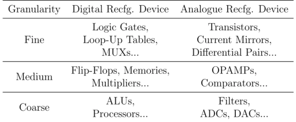
Due to specific needs, the arrangements of interconnects and reconfigurable fabric structure, where the fabric is defined as a set of reconfigurable building blocks, and the arrangement refers to an architecture, in reconfigurable de-vices can be different. However, their architectures can still be classified as linear, array, mesh, crossbar, data-path, etc. The details of these architec-tures are well introduced in Trefzer and Tyrrell’s book (Trefzer and Tyrrell, 2015), a book for reconfigurable hardware. On the configurable device, the configurable fabric structure is normally one of two types – homogeneous or heterogeneous structures. In a homogeneous structure, the configurable fabric is formed from identical configurable blocks, and these blocks are arranged in a regular fashion. In contrast, the heterogeneous structure means that, apart from some identical configurable blocks, the configurable fabric also contains a number of specialised blocks, known as hard macros. In addition to the reconfigurable fabric structures, another important parameter for the reconfigurable device is the granularity, which indicates the configurable level of the reconfigurable device. The granularity is usually defined at three levels. These are: fine-grained, medium-grained and coarse-grained. Table 2.1 shows that the configurable levels in digital and analogue configurable devices with
Table 2.1: The configurable levels in digital and analogue configurable devices with different granularities (Trefzer and Tyrrell, 2015)
Granularity Digital Recfg. Device Analogue Recfg. Device
Fine
Logic Gates, Transistors, Loop-Up Tables, Current Mirrors,
MUXs... Differential Pairs...
Medium Flip-Flops, Memories, OPAMPs, Multipliers... Comparators...
Coarse ALUs, Filters,
Processors... ADCs, DACs...
Recfg. = Reconfigurable MUXs = multiplexers
ALU = Arithmetic Logic Unit
ADC, DAC = Analog to Digital Converter, Digital to Analog Converter
different granularities.
2.2
Field Programmable Gate Array (FPGA)
2.2.1
Definition
The Field Programmable Gate Array, abbreviated to FPGA, is a pre-fabricated IC. It is a digital device which belongs to the category of reconfigurable digital devices, and has a number of pre-defined reconfigurable resources which allow the FPGA to be programmed or reprogrammed as any type of digital circuit or system after it has been fabricated (Brown and Rose, 1996).
It has been commonly considered that the modern FPGA era began with the first commercial FPGA introduced in 1985 – the Xilinx XC2064 FPGA, a static RAM, the SRAM (Pavlov and Sachdev, 2008), based FPGA that has 64 Configurable Logic Blocks (CLBs), 58 inputs and outputs (IOs), and
internal configurable fabric which is implemented as 4-input Look-Up Tables (LUTs), (Carter et al., 1986; Xilinx Inc., 1985; Kuon et al., 2007), which can be classified as fine-grained. Today, FPGAs have grown and developed significantly. A modern FPGA can contain more than 330,000 logic blocks, and have thousands of IOs (Kuon et al., 2007; Altera Corp., 2011b; Xilinx Inc., 2015a). As a result, FPGAs are widely utilised in digital systems, and used as a central configurable hub between different subsystems.
2.2.2
Applications
In the last two decades, by benefiting from the modern Very-Large-Scale Integration (VLSI) circuits technology (Weste and Harris, 2010), the FPGA scale has been increased significantly. FPGAs can be applied to a variety of applications. The applications of the FPGA can be summarised as follows:
1) From the hardware perspective, the FPGA can implement any logic circuits (Brown and Rose, 1996). In comparison with complex gate-level-ASIC-based digital PCBs (Printed Circuit Boards), the use of FPGAs can simplify the PCB, and lead to the FPGA being an all-in-one solution for digital logic. Moreover, modern FPGAs have a large number of configurable resources, including heterogeneous blocks; these enable the FPGA to build different digital subsystems, or even an entire system.
2) From the semiconductor industry perspective, due to the flexibility of the FPGA, FPGAs are widely used to verify new designs, or fast proto-typing designs. For example, the FPGA can be utilised to investigate timing and logic verification of a new digital design.
3) From the product perspective, the FPGA can implement high-speed, precision applications. These applications include: ultra high-speed interfaces, sophisticated controllers, high-high-speed signal processors,