American University in Cairo American University in Cairo
AUC Knowledge Fountain
AUC Knowledge Fountain
Theses and Dissertations6-1-2016
An electrocardiogram readout circuit based on CMOS operational
An electrocardiogram readout circuit based on CMOS operational
floating current conveyor
floating current conveyor
Nermine Maher EdwardFollow this and additional works at: https://fount.aucegypt.edu/etds
Recommended Citation Recommended Citation
APA Citation
Edward, N. (2016).An electrocardiogram readout circuit based on CMOS operational floating current conveyor [Master’s thesis, the American University in Cairo]. AUC Knowledge Fountain.
https://fount.aucegypt.edu/etds/623
MLA Citation
Edward, Nermine Maher. An electrocardiogram readout circuit based on CMOS operational floating current conveyor. 2016. American University in Cairo, Master's thesis. AUC Knowledge Fountain.
https://fount.aucegypt.edu/etds/623
This Thesis is brought to you for free and open access by AUC Knowledge Fountain. It has been accepted for inclusion in Theses and Dissertations by an authorized administrator of AUC Knowledge Fountain. For more information, please contact [email protected].
The American University in Cairo
School of Science and Engineering
An Electrocardiogram Readout Circuit Based On CMOS Operational Floating Current Conveyor
A Thesis Submitted to
Electronics and Communication Engineering Department
In partial fulfillment of the requirements for the degree of Master of Science
By Nermine Maher Edward Benyamin
Under the supervision of:
Prof. Yehea Ismail, Dr. Yehya Ghallab & Dr. Hassan Mostafa
February/2016 Cairo, Egypt
The American University in Cairo School of Science and Engineering (SSE)
An Electrocardiogram Readout Circuit Based on CMOS Operational Floating Current Conveyor
A Thesis Submitted by Nermine Maher Edward Benyamin Submitted to Department of Electronics
February /2016
In partial fulfillment of the requirements for The degree of Master of Science
has been approved by _______________________________
Thesis Supervisor Affiliation:
Date ____________________
_______________________________ Thesis first Reader
Affiliation:
Date ____________________
_______________________________ Thesis Second Reader
Affiliation: Date ____________________ _________________________________________ Department Chair Date ____________________ _________________________________________ Dean of SSE Date ____________________
i
To my Family,
ii
A dream doesn't become reality through magic; it takes sweat,
determination and hard work.
iii
Acknowledgment
First of all, I would like to thank God for all what He granted me in my life in every single aspect. I believe that God has provided me with blessings, care and guidance throughout my way.
I would like to thank my parents and my brother for their support and encouragement during my entire life. My dear husband, George, thanks very much for your great support. It is really difficult to express my deep gratitude, appreciation and love towards my family because of whom I seek my post-graduate studies.
I would like to show my gratitude to my supervisor Prof. Yehea Ismail for the great opportunity that he gave me. I would like to thank him for his support and guidance.
I would like also to express my gratitude to Dr. Yehya Ghallab and Dr. Hassan Mostafa for their help and great effort that they exerted during my research. They provided me with all the facilities that I need in my research.
Finally, I would like to express my gratitude to Dr. Ayman Elezabi and Dr. Karim Seddik for their support during my master’s studies.
iv
Abstract
Electrocardiogram (ECG) is used in diagnosing heart diseases. It is designed as integration between current-mode instrumentation amplifiers (CMIA) and low pass filter (LPF). Normal heart behavior can be identified simply by normal ECG that consists of signal while heart disorder can be recognized by having differences in the features of their corresponding ECG waveform.
A novel integrated CMOS-based operational floating current conveyor (OFCC) circuit is proposed. OFCC is a five port general purpose analog building block which combines all the features of different current mode devices such as the second generation current conveyor (CCII), the current feedback operational amplifier (CFA), and the operational floating conveyor (OFC).
The OFFC is modeled and simulated using UMC 130nm CMOS technology kit in Cadence with a supply voltage 1.2V. The ECG readout circuit has been designed using the proposed OFCC as a building block. The advantages of this: it is integrated, noise factor is small as the proposed OFCC has the lowest input noise voltage and the layout is simple as it is a single block that can be repeated several times.
v
Table of Contents
Abstract ... iv
List of Figures ... viii
List of Tables ... x
List of Symbols ... xi
List of Abbreviations and Nomenclature ... xiii
Chapter 1: Introduction ... 1
1.1 Introduction ... 1
1.2 Motivation ... 2
1.3 Thesis Outline ... 2
Chapter 2: Current mode devices ... 4
2.1 Introduction ... 4
2.2 Amplifier Circuits ... 4
2.3 Feedback Amplifiers and Feedback Topologies ... 5
2.4 Current mode devices ... 8
2.4.1 Current Conveyor ... 8
2.4.2 Current-Feedback Amplifier (CFA) ... 10
2.4.3 Operational Floating Conveyor (OFC) ... 11
2.4.4 Operational Floating Current Conveyor (OFCC) ... 13
2.5 Current Mode Devices vs. Voltage Mode Devices ... 15
2.5.1 CFA and VFA in Closed Loop Configuration ... 16
2.5.2 CFA and VFA in Open Loop Configuration ... 16
2.6 Noise in Amplifier Circuits ... 21
vi
Chapter 3: Proposed OFCC circuit ... 23
3.1 Introduction ... 23
3.2 Proposed Operational Floating Conveyor (OFC) ... 23
3.3 Proposed Design of OFCC ... 25
3.4 Simulation Results... 28
Chapter 4: Applications based on OFCC ... 32
4.1 Introduction ... 32
4.2 Non-inverting voltage amplifier ... 32
4.3 Current mode instrumentation amplifier ... 34
4.3.1 Designing using two CCII+ ... 35
4.3.2 Designing using three CCII+ ... 36
4.3.3 Designing using two op-amps working in conjunction with two CCII+ .... 37
4.3.4 Proposed integrated CMOS based CMIA ... 38
4.3.5 Simulation Results ... 41
4.4 Universal Filters ... 44
4.4.1 Introduction ... 44
4.4.2 Universal Filter with three inputs and single output ... 44
4.4.3 Simulation Results ... 46 4.5 Electrocardiography ... 49 4.5.1 Introduction ... 49 4.5.2 Circuit Design ... 50 4.5.3 Simulation Results ... 53 Conclusion ... 54 Future work ... 54 Appendix (A) ... 55 Universal Filter ... 55
vii
Low-Pass Filter: ... 55
Band-Pass Filter: ... 56
High- Pass Filter: ... 57
References ... 58
viii
List of Figures
Figure 2-1: Equivalent circuits for different amplifier circuits a) Current-Controlled Voltage Source b) Voltage-Controlled Voltage Source c) Voltage-Controlled Current
Source d) Current-Controlled Current Source ... 5
Figure 2-2: General negative feedback block diagram ... 6
Figure 2-3: First order BJT CC (CCI)... 8
Figure 2-4: Block diagram of CCI ... 9
Figure 2-5: Block diagram of CCII ... 9
Figure 2-6: Block Diagram of CFA ... 10
Figure 2-7: CFA equivalent circuit ... 11
Figure 2-8: Block diagram of OFC using CFA and current mirror ... 12
Figure 2-9: Block diagram of OFC using two CCII+ blocks and one noninverting ... 13
Figure 2-10: Block diagram of OFCC ... 13
Figure 2-11: Feedback amplifier (a) Inverting configuration (b) Non-inverting configuration ... 16
Figure 2-12: VFA equivalent circuit ... 17
Figure 2-13: VFA gain vs. Frequency ... 18
Figure 2-14: CFA gain vs. Frequency ... 19
Figure 2-15: Basic CFA circuit ... 20
Figure 2-16: Basic VFA circuit ... 21
Figure 2-17: Noise model of CMOS amplifier circuit ... 22
Figure 3-1: Proposed OFC circuit schematic ... 24
Figure 3-2: Proposed OFCC circuit schematic ... 27
Figure 3-3: Input terminals voltage tracking Vx/Vy ... 28
Figure 3-4: Input resistance rX ... 28
Figure 3-5: Input resistance rY ... 29
Figure 3-6: Open loop transimpedance ZT ... 29
Figure 3-7: Output terminals current tracking Iz+/Iw ... 30
ix
Figure 4-1: Non-inverting voltage amplifier configuration ... 32
Figure 4-2: Frequency characteristics of the voltage gain of the non-inverting voltage amplifier ... 34
Figure 4-3: Two CCII+ CMIA ... 35
Figure 4-4: Three CCII+ CMIA ... 36
Figure 4-5: Two CCII+ used in conjunction with two Op-amp CMIA ... 37
Figure 4-6: Proposed CMIA circuit ... 38
Figure 4-7: Gain for different values of RG ... 41
Figure 4-8: Second order universal filter ... 45
Figure 4-9: Magnitude response of the second-order universal filter in the Low-Pass Filter ... 46
Figure 4-10: Phase response of the second-order universal filter in the Low-Pass Filter 46 Figure 4-11: Magnitude response of the second-order universal filter in the Band-Pass Filter ... 47
Figure 4-12: Phase response of the second-order universal filter in the Band-Pass Filter 47 Figure 4-13: Magnitude response of the second-order universal filter in the High-Pass Filter ... 48 Figure 4-14: Phase response of the second-order universal filter in the High-Pass Filter 48
x
List of Tables
Table 2-1: Ideal Values of Input and Output impedances for Amplifiers ... 5
Table 2-2: The four feedback circuit topologies ... 7
Table 2-3: The closed loop gain of both CFA and VFA circuits ... 16
Table 3-1: Transistors aspect ratios ... 26
Table 3-2: Comparison between the proposed and other OFCC & OFC circuits ... 31
xi
List of Symbols
AV: Open loop voltage amplifier gain (Volt/Volt)
C: the effective output capacitance of the CCII+ CC: Compensation capacitor (Farad)
en: Input noise voltage (Volt/sqrt(Hz)) G: The closed loop gain
Gexact: The closed loop gain of the actual VFA.
Gideal: The closed loop gain of ideal amplifier.
hi1: The current tracking accuracy at Z+ terminal (IZ+)
hi2: The current tracking accuracy at Z- terminal (IZ-)
hV: The voltage tracking accuracy
IB: Input bias current (Ampere)
IW: Output current at terminal W
IZ+:Output current at terminal Z+
IZ-: Output current at terminal Z-
RF: Feedback resistance of CFA circuit (Ohm)
RG: the gain setting resistor
RL: Load resistance (Ohm)
RW: Feedback resistance of OFCC circuit (Ohm)
rX: Open loop input resistance (Ohm)
VIN: Input voltage (Volt)
VIO: Input offset voltage (Volt)
VOUT: Output voltage (Volt)
XERROR: Error signal (voltage or current)
XF: Output signal of the feedback network (voltage or current)
XIN: Error signal (voltage or current)
XOUT: Feedback signal (voltage or current)
ϵ
i+: The current tracking error at Z+ terminalxii
ϵ
v: The voltage tracking errorω
o: The natural frequencyQ: Quality factor
xiii
List of Abbreviations and Nomenclature
AC: Alternating current
BJT: Bipolar junction transistor BPF: Band pass filter
BW: Bandwidth
CCCS: Current controlled current source CCI: First generation current conveyor CCII: Second generation current conveyor
CCII+: Positive second generation current conveyor CCII-: Negative second generation current conveyor CCVS: Current controlled voltage source
CFA: Current feedback amplifier
CMOS: Complementary Metal Oxide Semiconductor CMRR: Common mode rejection ratio
dB: Decibel DC: Direct current
GBP: Gain bandwidth product GND: Ground (Zero voltage) HPF: High pass filter
Hz: Hertz kHz: 10E3 hertz KΩ: 10E3 ohm LOC: Lab-On-a-Chip LPF: Low pass filter mA: 10E-3 ampere MHz: 10E6 hertz
MOSFET: Metal-oxide-semiconductor field-effect transistor Rms: Root mean square
xiv VB1: DC bias voltage 1
VB2: DC bias voltage 2
VCCS: Voltage-controlled voltage source VCVS: Voltage-controlled current source VFA: Voltage feedback amplifier
1
Chapter 1: Introduction
1.1
Introduction
Heart diseases can be detected by using electrocardiogram (ECG). It yields by a nerve impulse stimulus to a heart, where the current is diffused around the surface of the body. The voltage drop will vary between µV to mV with an impulse variation. To record and display the ECG signal, this very small amplitude of impulse needs a couple of thousand times of amplification. In our design, the circuit is used to remove the noise and amplify the ECG signal [1].
Analog signal processing has an important role nowadays in both Lab-On-A-Chip (LOC) and communication systems. A LOC is a device that integrates one or more circuit performing different functions on a single chip. The main part of the LOC system is the read out circuit and to build this circuit, the amplifier circuit is needed. The amplifier circuit can be implemented using either a current mode or a voltage mode.
Digital and analog applications can be built using either bipolar junction transistor (BJT) or metal oxide semiconductor field effect transistor (MOSFET). In most of the applications nowadays MOSFET is used although it is slower than the BJT but on the other side it has lower power consumption. In addition, it is smaller in size than the BJT. Moreover, it permits large number of transistors to be packed together before heat problem happens [2–5].
For the voltage mode amplifier, the voltage signal is processed by the amplifier circuit. On the other hand, for the current mode amplifier the current signal is processed by the amplifier circuit.
Originally, voltage mode was used in amplifier circuits then current mode has started to take place [6]. Both the voltage and current modes can be used in the same applications but they have different characteristics. The advantages and disadvantages of both the voltage and current mode is discussed in chapter two.
2
There are different current mode circuits such as the first generation current conveyor (CCI), the second generation current conveyor (CCII), the current-feedback amplifier (CFA), the operational floating conveyor (OFC), and the operational floating current conveyor (OFCC).
This research presents a novel integrated CMOS current mode circuit, titled, operational floating current conveyor (OFCC).
1.2
Motivation
Design an integrated ECG read out circuit that have low input noise voltage with miniaturized blocks depending on current mode circuit; as there are many disadvantages in the voltage mode circuit such as having a constant gain-bandwidth product which affects the bandwidth of the amplifier by reducing and also the slew rate is low in the voltage mode circuit.
OFCC is a current mode circuit which overcomes the previous problems that occurs in the voltage mode circuits [7]. OFCC can be used in many applications, which will be discussed in chapter 4.
The OFCC circuit was firstly proposed by Khan. It was designed using discrete elements based on discrete BJTs and a commercial current-feedback amplifier (AD846) [8].
1.3
Thesis Outline
This thesis is organized in five chapters and one appendix as follows:
Chapter 1 presents a general introduction for the proposed amplifier circuit and describes the motivation of this work.
Chapter 2 discusses the differences between current and voltage mode devices. It presents the classification of the amplifiers in addition to the different types of current mode devices. The noise in amplifier circuits is presented as well.
In Chapter 3, the proposed design for OFCC circuit as well as a discussion comparing the advantages of the proposed OFCC with other existing circuits is presented.
3
Chapter 4 presents different applications based on OFCC, such as a non-inverting voltage amplifier, current mode instrumentation amplifier and universal filter. Moreover, an integrated ECG readout circuit based on OFCC as a building block is presented and discussed.
Chapter 5 contains the conclusion and the future work.
4
2
Chapter 2: Current mode devices
2.1
Introduction
In this chapter, a brief literature review of the different types of current mode devices like first generation current conveyor (CCI), second generation current conveyor (CCII), the current feedback amplifier (CFA), the operational floating conveyor (OFC), and the operational floating current conveyor (OFCC) is presented. Also, the difference between current mode (represented by CFA) and voltage mode (represented by VFA) devices is discussed. In addition, at the end of this chapter there is a brief discussion of the noise and its different sources as the noise in analog circuits is an important parameter which may affect the output signal.
2.2
Amplifier Circuits
The power and/or amplitude of a signal is increased using the electronic amplifier by taking power from the DC power supply and controlling the output to match the input signal shape but with larger amplitude.
The gain of the amplifier circuit can be defined as:
1. The ratio between the output and the input voltages. 2. Or the ratio between the output and the input power. 3. Or any other combination of current, voltage and power.
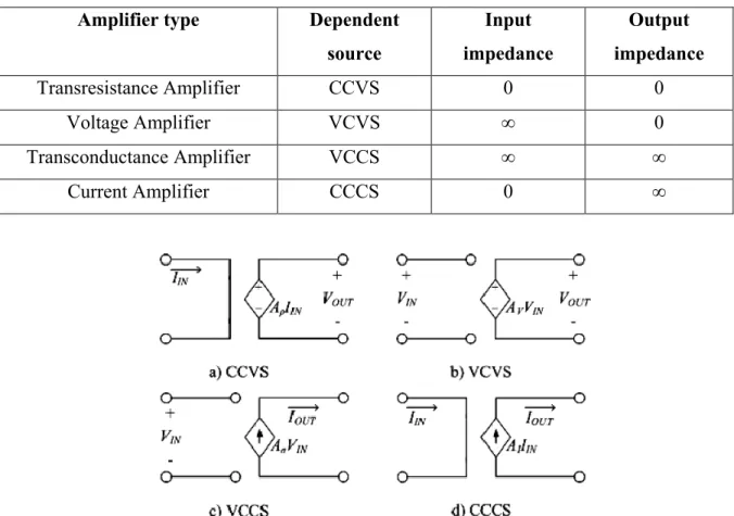
There are four types of amplifiers depending on the types of the input and output signals of the amplifiers. Table 2-1 shows the ideal input/output impedance values of the four amplifier types. Figure 2-1 shows an ideal equivalent circuit for each [9].
5
Table 2-1: Ideal Values of Input and Output impedances for Amplifiers
Amplifier type Dependent
source Input impedance Output impedance Transresistance Amplifier CCVS 0 0 Voltage Amplifier VCVS ∞ 0 Transconductance Amplifier VCCS ∞ ∞ Current Amplifier CCCS 0 ∞
Figure 2-1: Equivalent circuits for different amplifier circuits a) Current-Controlled Voltage Source b) Voltage-Controlled Voltage Source c) Voltage-Controlled
Current Source d) Current-Controlled Current Source [9]
2.3
Feedback Amplifiers and Feedback
Topologies
Normally, the amplifier circuit is used in a feedback configuration. The feedback system can be either positive feedback or negative feedback. Oscillator circuits use a positive feedback configuration. On the other hand, a stable amplifier circuit or an oscillator circuit under certain conditions (named as Barkhausen condition which depends on the loop gain of the feedback system) use negative feedback [10].
6
The advantages of the negative feedback system are: 1) it minimizes circuit distortion, 2) increases the bandwidth of the system, 3) improves the input and output impedance of the amplifier circuit and 4) lessens sensitivity of the output to the component variations. Figure 2-2 shows a general negative feedback block diagram.
Figure 2-2: General negative feedback block diagram [9]
XOUT: is the output signal of the system (voltage or current).
XIN: is the input signal of the system (voltage or current).
XERROR: is the error signal (input signal of amplifier).
XF: is the output signal of the feedback network.
A: is the open loop gain of the amplifier. β: is the gain of the feedback network. The overall gain of the system [9]:
𝑮 =
𝑿𝑶𝑼𝑻𝑿𝑰𝑵
=
𝑨𝟏+𝜷𝑨
(2-1)
βA: is defined as the loop-gain (1+ βA): is the amount of feedback G: is the closed loop gain
There are four feedback topologies according to the type of input and output signals of the system: Shunt-Shunt, Series-Series, Shunt-Series, and Series-Shunt topology. Table 2 summarizes amplifier type, amplifier gain, feedback gain, input signal type, output signal type and the closed loop gain for each type for the four feedback topologies [9].
7
Table 2-2: The four feedback circuit topologies [9]
Feedback Topology Input Connection Output Connection Input Signal Output
Signal Amplifier Type
Amplifier Gain Feedback Network Gain Closed Loop Gain Shunt- Shunt Feedback
Shunt Shunt Current Voltage Transimpedance
amplifier 𝐴𝜌 = 𝑉𝑂𝑈𝑇 𝐼𝐼𝑁 𝛽𝜎 = 𝐼𝐼𝑁 𝑉𝑂𝑈𝑇 𝐺 =𝑉𝑂𝑈𝑇 𝐼𝐼𝑁 = 𝐴𝜌 1 + 𝛽𝜎𝐴𝜌 Series- Series Feedback
Series Series Voltage Current Transconductance
amplifier 𝐴𝜎 = 𝐼𝑂𝑈𝑇 𝑉𝐼𝑁 𝛽𝜌 = 𝑉𝐼𝑁 𝐼𝑂𝑈𝑇 𝐺 =𝐼𝑂𝑈𝑇 𝑉𝐼𝑁 = 𝐴𝜎 1 + 𝛽𝜌𝐴𝜎 Shunt- Series Feedback
Shunt Series Current Current Current amplifier 𝐴𝐼 = 𝐼𝑂𝑈𝑇
𝐼𝐼𝑁 𝛽𝐼 = 𝐼𝐼𝑁 𝐼𝑂𝑈𝑇 𝐺 =𝐼𝑂𝑈𝑇 𝐼𝐼𝑁 = 𝐴𝐼 1 + 𝛽𝐼𝐴𝐼 Series- Shunt Feedback
Series Shunt Voltage Voltage Voltage amplifier 𝐴𝑉 = 𝑉𝑂𝑈𝑇
𝑉𝐼𝑁 𝛽𝑉 = 𝑉𝐼𝑁 𝑉𝑂𝑈𝑇 𝐺 =𝑉𝑂𝑈𝑇 𝑉𝐼𝑁 = 𝐴𝑉 1 + 𝛽𝑉𝐴𝑉
8
2.4
Current mode devices
The voltage mode devices suffer from having a constant gain-bandwidth product which means that when its gain starts to be increased, the bandwidth is decreased [11]. Current mode devices overcome the gain dependent bandwidth limitation so they have been used as active elements at the circuits that work at high frequencies.
2.4.1
Current Conveyor
Firstly the current conveyor was presented by Sedra in 1968, and then it was not vibrant what compensations the current conveyor introduced over the conventional op-amp [12]. After that subsequent formulation in 1970 [13] and Current Conveyor has become one of the most important building blocks of current mode circuits.
2.4.1.1
First Generation Current Conveyor (CCI)
The first circuit design of the CCI using bipolar transistors is shown in Figure 2-3. The input current at the input terminal X is conveyed to the output terminal Z (current tracking action) and at the same time there is a voltage tracking action between the two input terminals X and Y, as shown in Figure 2-4 [14].
9
Figure 2-4: Block diagram of CCI [14]
The operation of the CCI can be described using the following operation matrix equation:
[ 𝑰𝒀 𝑽𝑿 𝑰𝒛 ] = [ 𝟎 𝟎 𝟎 𝟏 𝟎 𝟎 𝟎 𝟏 𝟎 ] [ 𝑽𝒀 𝑰𝑿 𝑽𝒁 ] (2-2)
Wideband current measuring device and a negative impedance converter (NIC) were the first two applications using the CCI as a main block [15][16].
2.4.1.2
Second Generation Current Conveyor (CCII)
To improve the performance of the CCI, the second-generation current conveyor (CCII) was first introduced in [13][17]. It has two versions: the first one is the positive second generation current conveyor CCII+ which copies the current from a low output impedance node to a high output impedance node with the same phase and magnitude. The second one is the negative second generation current conveyor CCII- which also copies the current from low impedance to a high impedance node with the same magnitude but out of phase which is shown in Figure 2-5 [7].
10
The operation of the CCII can be described using the following operation matrix equation: [ 𝑰𝒀 𝑽𝑿 𝑰𝒛 ] = [ 𝟎 𝟎 𝟎 𝟏 𝟎 𝟎 𝟎 ±𝟏 𝟎 ] [ 𝑽𝒀 𝑰𝑿 𝑽𝒁 ] (2-3)
The input terminal Y has no input current which means that this terminal has high input impedance. The output current at terminal Z (𝐼𝑧) has the same magnitude as the input current at terminal X (𝐼𝑋) but it could be either in phase (CCII+) or out of phase (CCII-) with 𝐼𝑋.
2.4.2
Current-Feedback Amplifier (CFA)
Based on the CCII+, the current feedback amplifier (CFA) was firstly invented by David Nelson. It was designed by using the same topology as a CCII followed by a buffer, as shown in Figure 2-6 [18]-[19].
Figure 2-6: Block Diagram of CFA [18]
The CFA equivalent circuit is shown in Figure 2-7. It has two input terminals. The first input terminal is the inverting input terminal (X) with low input impedance ideally short circuit. The second input (Y) is the noninverting input terminal which has very high input impedance ideally open circuit.
11
The CFA circuit has a voltage-tracking action between its two input terminals X and Y. The buffer is used to model the voltage-tracking between the two input terminals of the CFA.
Figure 2-7: CFA equivalent circuit [20]
The output terminal VOUT has very low output impedance ideally short circuit.
The output voltage at this terminal is equal to the input current of the inverting terminal X times the total transimpedance of the current feedback amplifier ZT.
The CFA circuit can only work in a closed-loop configuration. Also, the CFA circuit has an optimum feedback resistance which improves its stability and at the same time it has an effect on its bandwidth [21].
2.4.3
Operational Floating Conveyor (OFC)
As the CCII became part of the current-feedback amplifier circuit construction; the CFA became a part of the construction of other circuits as the operational floating conveyor (OFC) that was introduced by Toumazou, Payne, and Lidgey in 1991 as shown in Figure 2-8 [22].
12
Figure 2-8: Block diagram of OFC using CFA and current mirror [22]
CFA circuit is the input stage of OFC circuit. The OFC circuit has two outputs; the first output terminal is the W terminal which is the output of the CFA. The second output terminal Z is the output of the current mirror circuit which has high output impedance. The current mirror controls the relation between the two output nodes which conveys the output current from node W to node Z. The basic difference between the OFC and CFA is the high output impedance at Z terminal which increases the OFC’s versatility and enables accurate closed-loop current tracking.
To improve bandwidth and provide smaller power dissipation a new design was proposed [23]. Also, it has simpler block diagram as shown in Figure 2-9 which makes it is easier to replace one block without much effect on the other blocks of the OFC realization. The first CCII+ is used to perform the voltage tracking at the input port between terminals Y and X. The second CCII+ is used to perform the required current tracking at the output port between terminals W and Z. To provide the output voltage at terminal W, the input current at terminal X is multiplied by the transimpedance amplifier gain.
13
Figure 2-9: Block diagram of OFC using two CCII+ blocks and one noninverting [23]
The operation of the OFC can be described using the following operation matrix equation: [ 𝑽𝑿 𝑰𝒀 𝑽𝑾 𝑰𝒁 ] = [ 𝟎 𝟏 𝟎 𝟎 𝟎 𝟎 𝟎 𝟎 𝒁𝑻 𝟎 𝟎 𝟎 𝟎 𝟎 −𝟏 𝟎 ] [ 𝑰𝑿 𝑽𝒀 𝑰𝑾 𝑽𝒁 ] (2-4)
2.4.4
Operational Floating Current Conveyor (OFCC)
The Operational Floating Current Conveyor (OFCC) is a five-port general purpose analog building block. The transmission properties of OFCC are similar to OFC and CFA as they have very low input impedance compared to the current conveyor circuits, but OFCC has additional high output impedance terminal which makes the device having better flexibility than the CFA and OFC [8].
2.4.4.1
OFCC Characteristics
The OFCC has two input terminals X &Y and has three output terminals W, Z+ and Z- as shown in Figure 2-10 [24].
Figure 2-10: Block diagram of OFCC [24]
Ix
Iz
14
The first input terminal X is a low impedance current input terminal. The second input terminal Y is a high input impedance voltage input terminal, as the OFCC has a current feedback amplifier at its input stage. On the other hand, the W terminal is the output voltage terminal of the current feedback amplifier, and has low output impedance. Both Z+ and Z- are high impedance output current terminals. The Z+ terminal has an output current equal in phase and magnitude to the W terminal. The Z- terminal has an output current which has the same magnitude as the W terminal’s current but is 180° out of phase.
2.4.4.2
OFCC Operation
There is an input current flowing at node X as it has very low input impedance (ideally zero). This current is multiplied by the open loop transimpedance gain (ZT) to
produce an output voltage at node W. There is a voltage tracking between the two input terminals (X and Y). The voltage at the high input impedance node Y appears at the second low input impedance node X.
The output terminal W has two kinds of output signals. The first output signal is the voltage which is equal to the input current of the input terminal X times the total transimpedance (ZT) of the circuit. The second output signal of the W terminal is the current: it flows from this node W and depends on the load of the circuit. This current is conveyed to node Z+ with the same magnitude and phase and to Z- with the same magnitude but 180° out of phase.
To conclude, the OFCC has two types of tracking actions. The first one is the voltage tracking between the two input terminals X and Y of the OFCC. The second one is the current tracking between the output terminals W, Z+, and Z- of the OFCC.
The operation of the exact OFFC can be described using the following operation matrix equation:
15 [ 𝑰𝒀 𝑽𝑿 𝑽𝑾 𝑰𝒁+ 𝑰𝒁−] = [ 𝟎 𝟎 𝟎 𝟎 𝟎 𝒉𝒗 𝟎 𝟎 𝟎 𝟎 𝟎 −𝒛𝑻 𝟎 𝟎 𝟎 𝟎 𝟎 𝒉𝒊𝟏 𝟎 𝟎 𝟎 𝟎 −𝒉𝒊𝟐 𝟎 𝟎][ 𝑽𝒀 𝑰𝑿 𝑰𝑾 𝑽𝒁+ 𝑽𝒁−] (2-5)
ℎ𝑣 is the voltage tracking and it is equal to (1 −∈𝑣), where ∈𝑣 is the voltage tracking error. Both ℎ𝑖1 and ℎ𝑖2 are the current tracking for both the Z+ and Z- terminals
respectively. The coefficient ℎ𝑖1 is equal to (1 −∈𝑖+) and ℎ𝑖2 is equal to(1 −∈𝑖−), where
∈𝑖+ and ∈𝑖− are the current tracking errors of the high output impedance terminals, Z+ and Z- respectively.
The operation of the ideal OFFC can be described using the following operation matrix equation: [ 𝑰𝒀 𝑽𝑿 𝑽𝑾 𝑰𝒁+ 𝑰𝒁−] = [ 𝟎 𝟎 𝟎 𝟎 𝟎 𝟏 𝟎 𝟎 𝟎 𝟎 𝟎 −𝒛𝑻 𝟎 𝟎 𝟎 𝟎 𝟎 𝟏 𝟎 𝟎 𝟎 𝟎 −𝟏 𝟎 𝟎][ 𝑽𝒀 𝑰𝑿 𝑰𝑾 𝑽𝒁+ 𝑽𝒁−] (2-6)
2.5
Current Mode Devices vs. Voltage Mode
Devices
Current mode and voltage mode devices each one of them have particular applications for which they are best matched. One of these applications is high speed application where the current mode devices are better due to the high slew rate capability of them.
An example of the current mode devices is the current feedback amplifier and an example of voltage mode devices is the voltage feedback amplifier. This section discusses the differences between them in two phases their closed loop characteristics & their open loop characteristics.
16
2.5.1
CFA and VFA in Closed Loop Configuration
Figure 2-11: Feedback amplifier (a) Inverting configuration (b) Non-inverting configuration [25]
Table 2-3: The closed loop gain of both CFA and VFA circuits [25]
Amplifier type Inverting closed loop Non-inverting closed loop
VFA 𝐺𝑖𝑑𝑒𝑎𝑙 =−𝑅𝐹 𝑅𝐼 𝐺𝑖𝑑𝑒𝑎𝑙 = 1 + 𝑅𝐹 𝑅𝐼 CFA 𝐺𝑖𝑑𝑒𝑎𝑙 =−𝑅𝐹 𝑅𝐼 𝐺𝑖𝑑𝑒𝑎𝑙 = 1 + 𝑅𝐹 𝑅𝐼
The closed loop configuration of an amplifier can be either inverting or non-inverting as shown in Figure 2-11. The amplifiers have the same ideal closed loop gain regardless of whether CFA or VFA amplifiers are used [25].
2.5.2
CFA and VFA in Open Loop Configuration
The differences between CFA and VFA start to appear in the open loop configuration. The most important difference between the two amplifiers is the gain-bandwidth product (GBP).
17
2.5.2.1
Gain-bandwidth product (GBP) of CFA and VFA
I. Gain bandwidth product of VFA
Figure 2-12: VFA equivalent circuit [25]
The equivalent circuit of the open loop voltage feedback amplifier is shown in Figure 2-12 [25]; its ideal circuit characteristics are infinite non-inverting and inverting input impedances, Zero output impedance and infinite open loop gain.
Taking into consideration the non-ideal characteristics of the VFA, the non-inverting closed loop gain for the voltage feedback amplifier shown in Figure 2-11 (b) is [25]:
𝑮
𝒆𝒙𝒂𝒄𝒕=
𝑽𝑶𝑼𝑻 𝑽𝑰𝑵=
𝑮𝒊𝒅𝒆𝒂𝒍 𝟏+𝑮𝒊𝒅𝒆𝒂𝒍 𝑨𝒗(𝒔) (2-7)𝐺𝑒𝑥𝑎𝑐𝑡: is the closed loop gain of the actual VFA.
𝐺𝑖𝑑𝑒𝑎𝑙: is the closed loop gain of ideal amplifier.
𝐴𝑣(𝑠): is the dominant pole open loop voltage gain of the VFA.
Due to the Miller effect the open loop gain is decreased with increasing frequency in VFA. Figure 2-13 shows the open loop gain of VFA gain versus the frequency [25]. The open loop gain is approximated by a single pole frequency dependent function. The closed loop gain is inversely proportional with the bandwidth of the amplifier circuit which means that when the closed loop gain increases the bandwidth of the amplifier decreases and vice versa. This is known as a constant gain bandwidth product in VFA circuits.
18
Figure 2-13: VFA gain vs. Frequency [25]
II. Gain Bandwidth Product of CFA
By referring to the open loop characteristics of the CFA in section 2.4.2 and taking into consideration the non-ideal characteristics of the CFA, the non-inverting closed loop gain for the current feedback amplifier shown in Figure 2-11 (b) is [25]:
𝑮
𝒆𝒙𝒂𝒄𝒕=
𝑽𝑶𝑼𝑻 𝑽𝑰𝑵=
𝑮𝒊𝒅𝒆𝒂𝒍 𝟏+ 𝑹𝑭 𝒁𝑻(𝒔) (2-8)𝐺𝑒𝑥𝑎𝑐𝑡: is the closed loop gain of the exact CFA.
𝐺𝑖𝑑𝑒𝑎𝑙: is the closed loop gain for ideal CFA.
𝑍𝑇(𝑠): is the single pole frequency dependent open loop transimpedance.
𝑅𝐹: is the feedback resistor for CFA.
The Miller effect decreases the open loop gain for the voltage mode amplifier. The absence of the Miller effect in CFA circuit enables the CFA frequency response to have a dominant pole frequency higher than the dominant pole in the case of the VFA.
19
The open loop transimpedance gain of the amplifier ZT(s) is shown in Figure 2-14
[25]. The bandwidth in case of the open loop current amplifier circuit is wider than that of the open loop voltage amplifier circuit. The CFA circuit will have a variable gain bandwidth product as increasing or decreasing the closed loop gain won’t affect the circuit bandwidth.
Figure 2-14: CFA gain vs. Frequency [25]
2.5.2.2
Bandwidth in VFA and CFA Circuits
The common topology of the CFA requires less gain stages than the VFA; this means less delay through the open-loop circuit which leads to higher bandwidth with the same power.
2.5.2.3
DC Characteristics of VFA and CFA Circuits
The input stage of the VFA is a differential amplifier and has four main advantages in terms of battery operation. Firstly, it has low input offset voltage (VIO).
Secondly, it has matched input bias currents (IB). Thirdly, it has high power supply
20
The input stage of the most common realization circuit of the CFA is a class AB buffer as shown in Figure 2-15 which has nonzero VIO and unmatched IB [25].
Figure 2-15: Basic CFA circuit [25]
2.5.2.4
Distortion in VFA and CFA Circuits
The overall distortion of the amplifier circuit is affected by the open loop distortion and the loop gain of the amplifier. The loop gain of the CFA circuit is much higher than that of VFA circuit, so the CFA tends to lead the VFA circuit. In the internal structure of the basic CFA circuit, as shown in Figure 2-15, each n-channel transistor has a corresponding p-channel transistor which is not the case in VFA circuits. This leads to having a low level of open loop distortion [25].
2.5.2.5
Slew Rate
For CFA that is shown in Figure 2-15, the compensation capacitor (Cc) charged and discharged by current which can be fed by both transistors M7 and M10. There is no limit (ideally) to the slew rate of the CFA as this current is a dynamic current.
21
For VFA that is shown in Figure 2-16 , it can be shown that the maximum current is bias current (IDC) with which the CCcan be charged or discharged [25].
Figure 2-16: Basic VFA circuit [25]
2.6
Noise in Amplifier Circuits
Noise in electronic circuits is a random signal. Noise sources can only be described by a probability density function (the most common probability density function is Gaussian,[26]) as they have amplitudes that vary randomly with time, so it is normally specified in root mean square value (RMS).
Noise can either be superimposed on the circuit by external sources or generated internally in the amplifier, from its associated passive components.
There are different types of noise in electronic circuits such as thermal noise, flicker noise, avalanche noise, burst noise, generation-recombination noise and shot noise. Thermal noise is the most effective noise parameter in the CMOS electronic circuits as it dominates noise’s value presented in the CMOS electronic circuit [27].
The input noise voltage (en) source for CMOS differential amplifier circuits dominates the noise effect as the input terminals have true high input impedances (gate terminal of the MOSFETs). The noise model in this case can be expressed by only one
22
voltage source at the noninverting input terminal of the amplifier as shown in Figure 2-17 [26].
Figure 2-17: Noise model of CMOS amplifier circuit [26]
2.7
Conclusion
The OFCC circuit is a promising current mode device as it combines the entire current mode device features. Both the current mode and voltage mode devices have the same closed loop gain in the ideal case, but they have different open loop characteristics. CFA have the following advantages compared to VFA:
Overcome the gain dependent bandwidth limitation.
Wider bandwidth.
Higher gain.
23
3
Chapter 3: Proposed OFCC circuit
3.1
Introduction
In this chapter, a novel integrated CMOS based operational floating current conveyor (OFCC) is presented. The proposed OFFC is implemented in two stages. The first stage is an OFC and the second one is a current steering circuit.
3.2
Proposed Operational Floating Conveyor
(OFC)
As described in chapter 2, there are two topologies that can be used in designing an operational floating conveyor. The first topology uses CFA circuit as a main part of the OFC circuit followed by a current mirror circuit as shown in Figure 2-8. The second one uses two CCII+ blocks, one noninverting transimpedance amplifier as shown in Figure 2-9. The second topology is the one that is used as the first stage in the proposed OFCC.
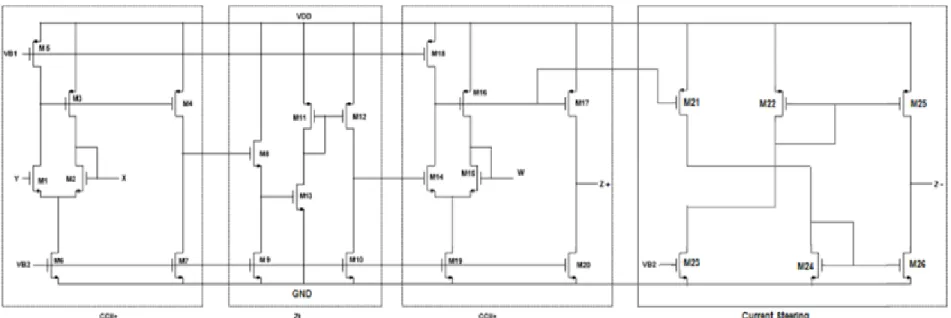
The proposed OFC circuit is shown in Figure 3-1. The first CCII+ (M1- M7) is used to perform the required voltage tracking action at the input port between terminals X and Y. In order to provide the output voltage at terminal W, the input current at terminal X is multiplied by the transimpedance amplifier gain ZT (M8- M13). The transimpedance
amplifier is working as follows; The input current at terminal X is mirrored by transistors M3, M4, M6 and M7 and the mirrored current will flow in the equivalent parasitic impedance of the gate terminal of M8, producing a voltage on it. This voltage is then amplified to produce the output voltage at terminal W. To perform the current following action at the output port between terminals W and Z, the second CCII+ (M14-M20) is used [23].
24
25
Taking into consideration the finite value of the transistor transconductance gm and drain
to source conductance gd and replacing each transistor by its small signal equivalent
circuit, the small signal voltage transfer gain from the Y terminal to the X terminal is [23]:
𝑨
𝒗=
𝒗𝒙 𝒗𝒚=
𝒈𝒎𝟏 𝒈𝒎𝟏+𝒈𝒅𝟏+𝒈𝒅𝟑(𝒈𝒅𝟏+𝟐𝒈𝒅𝟓) (𝒈𝒅𝟓+𝒈𝒎𝟑)(3-1)
The small signal input resistance seen at terminal X is [23]:
𝒓
𝒙=
(𝒈𝒅𝟏+𝟐𝒈𝒅𝟓)(𝒈𝒎𝟏+𝒈𝒅𝟏)(𝒈𝒎𝟑+𝒈𝒅𝟓)+𝒈𝒅𝟑(𝒈𝒅𝟏+𝟐𝒈𝒅𝟓)
(3-2) The small signal open loop transimpedance gain Zt is [23]:
𝒁
𝒕=
𝒈𝒎𝟏𝟐𝒈𝒎𝟏𝟑𝒈𝒎𝟏𝟒(𝒈𝒅𝟒+𝒈𝒅𝟕)(𝒈𝒅𝟏𝟐+𝒈𝒅𝟏𝟎)(𝒈𝒎𝟏𝟏+𝒈𝒅𝟏𝟑)(𝒈𝒎𝟏𝟒+𝒈𝒅𝟏𝟒+𝒈𝒅𝟏𝟔(𝒈𝒅𝟏𝟒+𝟐𝒈𝒅𝟏𝟖) (𝒈𝒅𝟏𝟖+𝒈𝒎𝟏𝟔)
(3-3)
The output resistance at terminal Z is [23]:
𝒓
𝒛=
𝟏𝒈𝒅𝟏𝟕+𝒈𝒅𝟐𝟎
(3-4)
3.3
Proposed Design of OFCC
OFCC consists of an OFC as a first stage and a current steering circuit as a second stage. The current steering circuit (M21-M24) is used to change the phase of the mirrored current by 180°. The steered current is mirrored by transistors M25 and M26 to produce IZ- as shown in Figure 3-2.
The circuit is designed and simulated using UMC 130nm CMOS technology kit in Cadence. The DC power supply used is 1.2V. The bias voltages VB1 and VB2 are equal 800mV and 380mV respectively. Design parameters of the transistors are reported in Table 3-1. The transistor aspect ratios (W/L) are in (μm/μm).
26
Table 3-1: Transistors aspect ratios
Transistor W/ L M1, M2 4/0.46 M3, M4, M11, M12 12.5/0.5 M14, M15 10/0.25 M16 30/0.12 M17 30/0.14 M5, M7, M10, M18 34.4/0.67 M20 10/0.12 M6, M8, M19 30/0.43 M9, M13 28/0.5 M21 30/0.14 M22, M23, M24 60/0.25 M25 160/0.35 M26 80/0.35
27
28
3.4
Simulation Results
The proposed circuit shown in Figure 3-2 is simulated using UMC 130nm CMOS technology kit in Cadence. The supply voltage of the proposed OFCC is 1.2V. The voltage tracking between X and Y terminals is presented in Figure 3-3. There is 0.4% error.
Figure 3-3: Input terminals voltage tracking Vx/Vy
The input resistance at terminal X is presented in Figure 3-4. It is equal 8.83Ω.
29
The input resistance at terminal Y is presented in Figure 3-5. It is equal 30.8E12Ω.
Figure 3-5: Input resistance rY
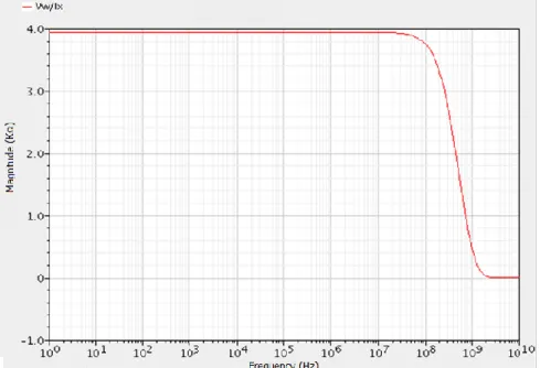
The frequency characteristics of the open loop transimpedance between X and W (Vw/Ix)
is presented in Figure 3-6. It is equal 3.94KΩ.
30
The output terminals current tracking Iz+/Iw and Iz-/Iw are presented in Figure 3-7 and
Figure 3-8 respectively. There is 0.5% and 0.8% error respectively.
Figure 3-7: Output terminals current tracking Iz+/Iw
31
Table 3-2 shows a performance comparison between the proposed and currently used OFCC and OFC. The proposed design of the CMOS based OFCC circuit has the lowest internal resistance which is equal to 8.83Ω compared to the other two designs. Also the proposed design has the highest 3dB frequency (bandwidth) which increased by 97.5% and 30.2% compared to others [7][23] respectively. OFC circuit [23] is the highest DC open loop transimpedance gain which is equal to 29.6KΩ, the proposed design is higher than the OFCC circuit presented in [7] by 0.94KΩ. The power consumption in the proposed design is equal to 1.5mW which is higher than [7] by 0.4mW. However, OFCC presented in [7] is designed based on 90nm CMOS technology. The proposed design has a lower power consumption compared to [23] by about 0.9mW.
Table 3-2: Comparison between the proposed and other OFCC & OFC circuits
OFC & OFCC Reference Proposed [7] [23]
Technology 130nm 90nm 500nm
Supply (V) +1.2 +1.2 ±1.5
Input voltage dynamic range (V) 0.5 to 0.9 0 to 0.8 -0.4 to 1.2
Input resistance rx (Ω) 8.83 20 30.2
-3dB frequency (Bandwidth) 1.2GHz 30MHz 826MHz
DC open loop transimpedance (kΩ) 3.94 3 29.6
32
4
Chapter 4: Applications based on OFCC
4.1
Introduction
OFCC is a versatile analog device as both its input and output ports are floating. It is designed to be used in a closed loop implementation with current feedback from terminal W to terminal X. There are many applications that can be designed in a closed loop such as: inverting voltage amplifier, non-inverting voltage amplifier, transresistance amplifier, transconductance amplifier, current mode instrumentation amplifier (CMIA) and universal filter. This chapter discusses only four applications based on OFCC, non-inverting voltage amplifier, CMIA, universal filter and electrocardiogram (ECG).
4.2
Non-inverting voltage amplifier
The non-inverting voltage amplifier is a voltage controlled voltage source (VCVS) and is shown in Figure 4-1 [23].
Figure 4-1: Non-inverting voltage amplifier configuration [23]
The voltage gain can be expressed as follows:
𝑨
𝒗=
𝑽𝒐𝑽𝒊
= 𝟏 +
𝑹𝟐
33
The single pole model transimpedance gain by taking the effect of the finite transimpedance gain, 𝑍𝑡, and using the finite transimpedance single pole model can be expressed as:
𝒁
𝒕(𝒔) =
𝒁𝒕𝒐𝟏+𝒔
𝒘𝒐
(4-2)
𝑍𝑡𝑜: DC open loop transimpedance gain
𝑤𝑜: transimpedance cutoff frequency
The transimpedance gain 𝑍𝑡(𝑠) for high frequency applications:
𝒁
𝒕(𝒔) =
𝟏 𝒔𝑪𝒑 (4-3)𝑪
𝒑=
𝟏 𝒁𝒕𝒐𝒘𝒐 (4-4) Applying KCL at terminal X:𝑰
𝒙=
𝑽𝒊−𝑽𝟎 𝑹𝟐+
𝑽𝒊 𝑹𝟏 (4-5)Substituting by Ix = Vo/Zt in eq. (4-5), the non-inverting voltage amplifier gain is given
by:
𝑨
𝒗=
𝑽𝒐 𝑽𝒊= (𝟏 +
𝑹𝟐 𝑹𝟏)
𝟏 𝟏+ 𝑹𝟐 𝒁𝒕(𝒔)= (𝟏 +
𝑹𝟐 𝑹𝟏) 𝜺(𝒔)
(4-6)𝜀(𝑠): the error function
𝜺(𝒔) =
𝟏𝟏+ 𝑹𝟐
𝒁𝒕(𝒔)
(4-7)
By substituting from eq. (4-3) into eq. (4-7), the error function will be reduced to:
𝜺(𝒔) =
𝟏34
The circuit is simulated using UMC 130nm technology kit in Cadence. R1=10K
and R2= 5K, 90K and 200K. The different gains of the differential voltage amplifier are
shown in Figure 4-2. For R2= 5K, 90K and 200K the gain has an error equal to 0.67%,
0.3% and 0.4% respectively.
Figure 4-2: Frequency characteristics of the voltage gain of the non-inverting voltage amplifier
4.3
Current mode instrumentation amplifier
Instrumentation amplifiers are very important as they are used in many fields, such as medical instrumentation, the read-out circuit of biosensors, signal processing and data acquisition. One of the most important areas is the lab-on-a-chip, which requires the integration of the actuation and sensing parts, as well as the read-out circuit in a single chip. Lab-on-a-chip needs a wide bandwidth instrumentation amplifier to suppress any unwanted common-mode signal and amplify the differential signals [28].35
There are two types of instrumentation amplifiers, they are the conventional voltage-mode instrumentation amplifiers (VMIAs) based on a voltage operational amplifier and current-mode instrumentation amplifiers (CMIAs) based on a current operational amplifier. As a result of the fixed gain bandwidth product of the operational amplifier, VMIAs have narrow bandwidth that is highly dependent on the gain. They need precise resistor matching to attain high common-mode rejection ratio (CMRR) [29– 31].
On the other hand, CMIAs have better performance and wider frequency range of operation compared to VMIAs. CMIAs also do not require matched resistors [32]. Second-generation current conveyor (CCII) was used before in CMIAs.
4.3.1
Designing using two CCII+
CMIAs were designed using two CCII+ [33] as shown in Figure 4-3. This two CCII+ topology introduces a simple and symmetric circuit topology, and has a high CMRR without requiring matched resistors.
Figure 4-3: Two CCII+ CMIA [33] Vin1 Vin2 X Z Y CCII+ (1) RG Z X Y CCII+ (2) Vo RL Y
36
The frequency dependent differential gain can be expressed as follows [33]:
𝑨
𝒅(𝒔) =
𝒗𝒐 𝒗𝒊𝒏𝟏−𝒗𝒊𝒏𝟐=
𝑹𝑳 𝑹𝑮+𝟐𝑹𝑿.
𝟏 𝟏+𝒔𝑪𝑹𝑳 (4-9)RX: the equivalent input resistance at the X terminal
RG: the gain setting resistor
C: the effective output capacitance of the CCII+ RL: the load resistor
4.3.2
Designing using three CCII+
CMIAs were designed using three CCII+ [34] as shown in Figure 4-4. Comparing to the two CCII+ approach higher CMRR and higher differential gain will be reached using the three CCII+ approach.
Figure 4-4: Three CCII+ CMIA [34]
The differential gain can be computed as follows [34]:
𝑨
𝒅(𝒔) =
𝒗𝒐 𝒗𝒊𝒏𝟏−𝒗𝒊𝒏𝟐=
𝟐𝑹𝑳 𝑹𝑮+𝟐𝑹𝑿.
𝟏 𝟏+𝒔𝑪𝑹𝑳(4-10) X Y Z Vin2 Vin1 Y X Z Y X Z RG Vo RL CCII+ (1) CCII+ (2) CCII+ (3)
37 Vin2 Y X Z CCII+ (1) RL Y X Z CCII+ (2) RG Op-Amp Vin1 Vo Op-Amp
As shown in (4-9) and (4-10) the differential gain of both designs is inversely proportional to RX and the accuracy is limited by the tolerance of RX, which is low. To
improve the accuracy of the CMIA, two op-amps working in conjunction with two CCII+ [35] are used.
4.3.3
Designing using two op-amps working in conjunction
with two CCII+
Figure 4-5 shows CMIA that was designed using two op-amps working in conjunction with two CCII+.
Figure 4-5: Two CCII+ used in conjunction with two Op-amp CMIA [36]
The differential gain of this CMIA is given as follows [35]:
𝑨
𝒅(𝒔) =
𝒗𝒐 𝒗𝒊𝒏𝟏−𝒗𝒊𝒏𝟐=
𝑹𝑳 𝑹𝑮.
𝟏 𝟏+ 𝒔𝝉 𝟏+𝑲𝜷 (4-11) β= RG / (2RX+RG)38
𝜏: the time constant of the op-amp K: the low-frequency gain of the op-amp
As shown in (4-11), the low-frequency gain is independent of RX, however the bandwidth
is dependent on RX. This approach suffers from higher power consumption and a more
complicated circuit topology when compared with the topologies shown in Figure 4-3 and Figure 4-4. On the other hand, it has a more accurate low-frequency differential gain than the two CCII+ based CMIA.
4.3.4
Proposed integrated CMOS based CMIA
The proposed CMIA circuit is based on operational floating current conveyor (OFCC), which has flexible characteristics with respect to other current-mode or voltage mode devices [36]. It consists of two OFCCs, two feedback resistors (RW1 and RW2), a
gain-determined resistor (RG), and a ground load (RL), as shown in Figure 4-6.
Figure 4-6: Proposed CMIA circuit [36]
I2 RW2 RG RL Vo Y X Z- W CZ- VB Vin2 X Y Z- Z+ W RW1 Vin1 VA I1 IX OFCC (1) OFCC (2) Z+ CZ+
39
The negative feedback resistor between W and X allows the OFCC to operate at a positive or negative current-conveyor while simultaneously reducing the input resistance at X port [37]. Also, the dc stability as well as the transfer function accuracy is improved due to the negative feedback [32][35].
Taking into consideration both the voltage and current tracking errors of the OFCC, the current tracking error between ports X, Z+, and Z- is [38]:
𝜶 = 𝟏 − 𝜺
+ (4-12)𝜸 = 𝟏 − 𝜺
−(4-13)
𝜀
+:the finite current tracking error at the high impedance output Z+𝜀
−:the finite current tracking error at the high impedance output Z-The port currents can be given as [38]:
𝒊
𝒛+= 𝜶𝒊
𝒙(4-14)
𝒊
𝒛−= 𝜸𝒊
𝒙(4-15)
The voltage tracking error between ports X and Y [38]:
𝜷 = 𝟏 − 𝜺
𝑽(4-16)
εV: the finite voltage tracking error at the low impedance X from the high input
impedance node Y.
The voltage at nodes 𝑣𝐴 and 𝑣𝐵can be given as [38]:
𝒗
𝑨= 𝜷
𝟏𝒗
𝒊𝒏𝟏(4-17)
𝒗
𝑩= 𝜷
𝟐𝒗
𝒊𝒏𝟐(4-18)
The resulting current 𝑖𝑥 [38]:
𝒊
𝒙=
𝒗𝑨−𝒗𝑩40
𝒊
𝒙=
(𝜷𝟏𝒗𝒊𝒏𝟏−𝜷𝟐𝒗𝒊𝒏𝟐)𝑹𝑮
(4-20) The output terminals currents [38]:
𝒊
𝟏= 𝜶
𝟏𝒊
𝒙=
𝜶𝟏(𝜷𝟏𝒗𝒊𝒏𝟏−𝜷𝟐𝒗𝒊𝒏𝟐)𝑹𝑮
(4-21)
𝒊
𝟐= 𝜸
𝟐𝒊
𝒙=
𝜸𝟐(𝜷𝟏𝒗𝒊𝒏𝟏−𝜷𝟐𝒗𝒊𝒏𝟐)
𝑹𝑮
(4-22) The output voltage [38]:
𝒗
𝒐(𝒔) = (𝒊
𝟏+ 𝒊
𝟐)(𝑹
𝑳//
𝟏 𝒔𝑪𝒁)
(4-23) and
𝑪
𝒁= 𝑪
𝒁++ 𝑪
𝒛−(4-24) then,
𝒗
𝒐(𝒔) =
(𝜷𝟏𝒗𝒊𝒏𝟏−𝜷𝟐𝒗𝒊𝒏𝟐)(𝜶𝟏+𝜸𝟐)𝑹𝑳 𝑹𝑮(𝟏+𝒔𝑪𝒁𝑹𝑳)(4-25)
When Vin1=Vin2=Vcm, the common-mode gain is equal [38]:
𝑨
𝑪𝑴(𝑺) =
𝒗𝒐𝒗𝒄𝒎
=
(𝜷𝟏−𝜷𝟐)(𝜶𝟏+𝜸𝟐)𝑹𝑳
𝑹𝑮(𝟏+𝒔𝑪𝒁𝑹𝑳)
(4-26)
For ideal OFCCs,
𝜶𝟏 = 𝜶𝟐= 𝜸𝟏= 𝜸𝟐 = 𝜷𝟏 = 𝜷𝟐 = 𝟏
Then, the output voltage [38]:
𝒗
𝒐(𝒔) =
𝟐𝑹𝑳(𝒗𝒊𝒏𝟏−𝒗𝒊𝒏𝟐)41 The output differential gain [38]:
𝑨
𝒅(𝒔) =
𝒗𝒐𝒗𝒊𝒏𝟏−𝒗𝒊𝒏𝟐
=
𝟐𝑹𝑳
𝑹𝑮(𝟏+𝒔𝑪𝒛𝑹𝑳)
(4-28)
From (4-28), it’s clear that the differential gain can be adjusted and controlled by RG
without affecting the bandwidth of the CMIA.
4.3.5
Simulation Results
The circuit is designed and simulated using UMC 130nm technology kit in Cadence. The DC power supply used is 1.2 Volt.
A. Differential Gain Measurements
To measure the differential gain of the proposed CMIA, we connected the input voltage to Vin1 and connected Vin2 to ground. Resistors RW1 and RW2 were set to 6.5K, RL
was set to 1K and RG was tested at different values. Figure 4-7 shows the gain for
different values of RG.
Figure 4-7: Gain for different values of RG
RG=50Ω
RG=100 Ω
RG=500 Ω
42
The proposed topology for RL/RG=10 exhibits a differential gain equal 20 with
bandwidth 32.7MHz which its gain is double the CMIAs in [33][35] and has bandwidth higher than other CMIAs by 30.7 MHz as shown in Table 4-1. However, its gain is similar to the CMIA given in [34][38]. Moreover, the proposed topology is independent of RX and the gain is independent of the bandwidth.
B. CMRR Measurements
To measure the CMRR of the circuit, two identical ac signal source Vcm are
connected in series with the inputs. An AC analysis is carried out for finding the CMRR [39].
𝒗𝒐
𝒗𝑪𝑴
=
𝟏
𝑪𝑴𝑹𝑹 (4-29)
The proposed CMIA exhibits a CMRR magnitude 61dB and bandwidth 292MHz which is independent of gain. It has the lowest CMRR as it is lower than [38] by 19.7% on the other hand the bandwidth of the CMRR is the highest as it is higher than [38] by 57.8%.
The input noise voltage for the proposed CMIA is lower than [38] by 99.98%. It has the widest dynamic range and highest signal-to-noise ratio compared to the other circuits. It is an integrated circuit compared to others which are discrete [33] [34] [35] [38].
43
Table 4-1: Comparison between the proposed and other CMIA circuits
CMIA Reference
Differential Gain For RL/RG=10 CMRR For RL/RG =10 Input noise
voltage nV/√Hz for RL/RG =10 Number of building blocks used Type of integration Mag (Value) -3 dB Freq (BW) Gain BW (MHz) Gain varies with BW Mag (dB) -3 dB Freq (BW)
[33] 9.09 2MHz 18.18 yes 65 16kHz 20.6 2 CCII+ Discrete
[35] 10 2MHz 20 yes 65 16kHz 22.4 2 CCII+
2Op-amp Discrete [34] 17.8 1.4MHz 24.92 no 73 65kHz 19.8 3 CCII+ Discrete
[38] 20 1.2MHz 24 no 76 185kHz 15.2 2 OFCC Discrete
44
4.4
Universal Filters
4.4.1
Introduction
Second-order universal filter with three inputs and a single output is selected to test the efficiency of the designed OFCC circuit [40] and is used in designing ECG as will be mentioned in section 4.5.
4.4.2
Universal Filter with three inputs and single output
Figure 4-8 shows the proposed second order universal filter with three inputs and one output. The analysis of the transfer function is shown in Appendix A.
In general the transfer function is:
𝑽
𝒐=
𝒔𝟐𝑪𝟏𝑪𝟐𝑪𝟑𝑹𝟏𝑹𝟐𝑹𝟑𝑽𝟏+𝒔𝑪𝟐𝑹𝟐𝑹𝟑𝑽𝟐+𝑹𝟏𝑽𝟑𝒔𝟐𝑪𝟏𝑪𝟐𝑪𝟑𝑹𝟏𝑹𝟐𝑹𝟑+𝒔𝑪𝟐𝑹𝟐𝑹𝟑+𝑹𝟏 (4-30)
This circuit can analyze three types of filters, which are low pass, band pass and high pass filters. These can be done by changing the input node connections.
For high pass filter, V2 and V3 are grounded and the input signal is V1.
For band pass filter, V1 and V3 are grounded and the input signal is V2.
For low pass filter, V1 and V2 are grounded and the input signal is V3.
The natural frequency (ωo) and the quality factor (Q) are expressed as follows:
𝝎
𝒐= √
𝑪 𝟏 𝟏𝑪𝟐𝑹𝟐𝑹𝟑(4-31)
𝑸 = 𝑹
𝟏√
𝑪 𝑪𝟏 𝟐𝑹𝟐𝑹𝟑(4-32)
Without affecting the performance of the OFCC circuit, controlling the natural frequency and the quality factor values can be done as they are independent of the feedback resistor Rw.
45 R2 R3 RW OFCC (2) Y X Z+ Z- W C1 Vo V1 X Y Z- Z+ W RW C2 R1 V2 V3 OFCC (1)
46
4.4.3
Simulation Results
The resistance R1 and R3 are set to 3.6KΩ, R2 was set to 300Ω and Rw was set to
1.5K. Also C1 and C2 are set to 19nF and 225nF respectively. The ωo is 14.72Kr/s and the
Q is equal to 1.01.
4.4.3.1
Low pass Filter
Figure 4-9: Magnitude response of the second-order universal filter in the Low-Pass Filter
Figure 4-10: Phase response of the second-order universal filter in the Low-Pass Filter
47
4.4.3.2
Band pass Filter
Figure 4-11: Magnitude response of the second-order universal filter in the Band-Pass Filter
Figure 4-12: Phase response of the second-order universal filter in the Band-Pass Filter
48
4.4.3.3
High pass Filter
Figure 4-13: Magnitude response of the second-order universal filter in the High-Pass Filter
Figure 4-14: Phase response of the second-order universal filter in the High-Pass Filter
49
4.5
Electrocardiography
4.5.1
Introduction
Electrocardiography (ECG) is the analysis of the electrical activity of human’s heart over a period of time. The human body contains cells that act like batteries. Biopotentials are small electric potentials that is created from different ions outside and inside the cells’ membranes [41]. Figure 4-15 shows the depolarization and repolarization of the cell that exist when there is a disturbance in a biopotential.
Figure 4-15: Depolarization and repolarization when there is a disturbance
Electrocardiograph (ECG) signals are made of the action potentials from different nodes in the heart as shown in Figure 4-16. Their measurement can be done by using the electrocardiogram (ECG).
50
Figure 4-16: ECG signal [41]
4.5.2
Circuit Design
The main function of the ECG is to filter noise of the small signal measured from the heart then to amplify it as their range vary from the microvolt to the millivolt. So, the ECG is composed of two LPF and one CMIA as shown in Figure 4-17.
51
Figure 4-17: Proposed ECG circuit
LPF LPF R=1k R=1k C=47n R=1k R=1k C=47n CMIA V o in1 in2
52
4.5.2.1
Filter
The ECG signal is composed of noise that exist from the body and environment so using low pass filter helps to remove this noise. In designing the filter, we use the low pass filter as discussed in chapter 4. The resistors R1 and R3 are set to 4KΩ, R2 is set to
2kΩ and Rw is set to 500. Also C1 and C2 are set to 10uF and 10pF respectively. The
frequency will be 55 Hz as shown in Figure 4-18.
Figure 4-18: Low pass filter used in ECG
4.5.2.2
Instrumentation Amplifier
ECG signals vary from the microvolt to the millivolt range. The signal measured has to be amplified due to this small rang. In addition, to eliminate large offset signals the amplifier should have a high common mode rejection ratio. The instrumentation amplifier that is used in designing the ECG is previously discussed in chapter 4. Resistors RW1 and
RW2 are set to 1KΩ, RL and RG are set to 10KΩ and 50Ω respectively. Also C1 and C2 are
![Figure 2-2: General negative feedback block diagram [9]](https://thumb-us.123doks.com/thumbv2/123dok_us/1871312.2773121/23.918.206.714.238.485/figure-general-negative-feedback-block-diagram.webp)
![Figure 2-8: Block diagram of OFC using CFA and current mirror [22]](https://thumb-us.123doks.com/thumbv2/123dok_us/1871312.2773121/29.918.323.598.135.487/figure-block-diagram-ofc-using-cfa-current-mirror.webp)
![Figure 2-9: Block diagram of OFC using two CCII+ blocks and one noninverting [23]](https://thumb-us.123doks.com/thumbv2/123dok_us/1871312.2773121/30.918.174.745.140.320/figure-block-diagram-ofc-using-ccii-blocks-noninverting.webp)
![Table 2-3: The closed loop gain of both CFA and VFA circuits [25]](https://thumb-us.123doks.com/thumbv2/123dok_us/1871312.2773121/33.918.128.786.581.727/table-closed-loop-gain-cfa-vfa-circuits.webp)
![Figure 3-1: Proposed OFC circuit (schematic) [23]](https://thumb-us.123doks.com/thumbv2/123dok_us/1871312.2773121/41.1188.152.1076.139.560/figure-proposed-ofc-circuit-schematic.webp)