EAI
®---
ELECTRONIC ASSOCIATES, INC. Long Branch, New JerseyTR-48 ANALOG COMPUTER
OPERATORS MANUAL
Reprinted October 1963
© ELECTRONIC ASSOCIATES, INC. 1963 ALL RIGHTS RESERVED
TR-48 COMPUIER CONI'ENI'S
SEafION I INTRODUCT ION
...
SECl'ION II - THE TR-48 COMPUl'ER
...
1 •
2.
6.
GENERAL DESCRIFl'ION OF THE TR-48
...
OPERATING CUNSIDERATIONS
...
.b..
£..
.dr..
Preliminary Operating Considerations
...
Pre-Patch Panel Insertion and Removal
...
Amplifier Balance
.
... .
Changing Computational Components •••••••••••••••••••••
MONITURING AND CONTROL ••••••••••••••••••••••••••••••••••••
.§.. Signal Selector •••••••••••••••••••••••••••••••••••••••
Digital Voltmeter
...
Multi-Range Voltmeter •••••••••••••••••••••••••••••••••
Computer MODE •••••••••••••••••••••••••••••••••••••••••
Overload Indicators
...
Trunks
...
~... .
Readou:t Devices
...
ATTENUATORS • • • • • • • • • • • • • • • • • • • • • • • • • • • • • • • • • • • • • • 0 • • • • • • • •
OPERATIONAL AMPLIFIER •••••••••••••••••••••••••••••••••••••
General Considerations" ••••••••••••••••••••••••••••••••
.b..
TR-48 Operational Amplifier 6.514 •••••••••••••••••••••QU.ARTER-SQUARE
MU.ur
IPLIER...•...
.§.. Multiplication ••••••••••••••••••••••••••••••••••••••••
~. Division ••••••••••••••••••••••••••••••••••••••••••••••
7.
8.
9.
CONl'ENT'S (Cont)
DIODE FUNCTION GENERATORS •••••••••••••••••••••••••••••••
x
2 Diode Function Generator...
,b.. Log X Diode Function Generator ••••••••••••••••••••••£.. 1/2 Log X Diode Function Generator
.
... .
~. Variable Diode Function Generator.
... .
REP:m'IT DIE OPERAT ION (REP-oP)
...
.
COMPUTATIONAL ACCESSORIES •••••••••••••••••••••••••••••••
Signal Comparator
40.404 ••••••••••••••••••••••••••••
Function Switches'
...
SECTION III - BASIC PROGRAMMING
...
1.
SY3rEM EQUATIONS •••••••••••••••••••••••••••••••
~••••••••
2. THE
BOOXSl'RAP
1'-1E:I'HOD.
... .
SC~IN'G •••••••••••••••••••••••••••••••••••••••••••••••••
Amplitude Scaling •••••••••••••••••••••••••••••••• 0 • •
.b..
T ilne Scaling ••••••••••••••••••••••••••••••••••••••••4.
COMPUl'ER
C IRC UITDIAGRAM
.
... .
PROBLEM CHECK PROCEDURES
...
6. PROGRAMMING A
LINEAR
PROBLEM...
Problem Description •••••••••••••••••••••••••••••••••
.b,. Preliminary Considerations ••••••••••••••••••••••••••
£.. Scali.ng ••••• 0 • • • • • • • • • • • • • • • • • • • • • • • • • • • • • • • • • • • • • • •
.9,. Computer Circuit Diagram •••••••••••••••••••••••••••• Check Procedures and Set Up Sheets ••••••••••••••••••
C01lTENTS (Cont)
7. A NON-LINEAR PROBLEM ••••••••••••••••••••••••••••••••••••
~
40
.sa... Problem Description ••••••••••••••••••••••
0...
40Q.
Preliminary Considerations ••••••••••••••••••••••••••41
,g". Scaling. • • • .. .. • • • • • • • • • • • • • • • .• • • • • • • • • • • • • • • • • • • • • • • • 42
g.
Computer Diagram •••••••••••••••••••••••••••••••••••• 43~. Checking the Computer Program ••••••••••••••••••••••• 43
SECTION IV - ADVANCED TECHNIQUES •••••••••••••••••••••••••••••••••
46
1. FUNGrrON GENERATION •••••••••••••••••••••••••••••••••••••
46
A.
Analytic Functions ••••••••••••••••••••••••••••••••••46
~. Techniques Involved in Using the DFG •••••••••••••••• 47
£. Curve Follo'Wer and BIVAR o • • • • • • • • • • • ~ • • • • • • • • • • • • • • • 2. TRANSFER FUNCTION SIMULATION • • • • • • • • • • • • • • 0 • • • • • • • • • • • • •
.§.... Transfer FWlction Simulation Using standard Amplifiers
47
48
and Potentiometers ... 48
.Q.. Transfer Function Simulation Using RC Net'Works ...
0 .
49
3.
REPRESENTATION OF DISCONTINUITIES •••••••••••••••
0...
50
4..
PARTIAL DIFFERENTIAL
EQU~IONS...
00 .... 00...
52THE .METHOD. OF Sl'EEPEsr DESCENT S • • • • • • • • • • • • • • • • • 0 . 0 0 0 . 0 0 54
APPENDIX 1 COMPUTER
SYMBOLS ••••••••••••••••••
0 • • • • • • • • • 0 0 • • 0 0 0 . AI-1APPENDIX 2 SIMPLE
CIRCUIT
S USING AMPLIFIERS AND POTENTIOME.rERS .. AI 1-1APPENDIX J QUARTER-8QU.ARE MUI!r
IPLIER ClRCUlT S ...
0 • • • • • AIII-1APPENDIX 4 - X2 DFG
CIRCUITS
• • • • • • • • • • • • • • • • • 0 • • 0 0 . 0 • • • 0 0 0 . 0 0 0 0 0 AN-1CONTENT S (Cont)
~
APPENDIX
5 -
LOG X AND 1/2 LOG X DFG CIRCUITS •••••••••••••••••••••
AV-1
APPENDIX
6 - VDFG CIRCUITS •••
~...AVI-1
APPENDIX
7 - TRANSFERFUNGrION SIMULATION ••••••••••••••••••••••••• AVII-1
APPENDIX
8 -REPRESENTATION OF DISCONTINUITIES •••••••••••••••••••• AVIII-1
APPENDIX
9 -BIBLIOGRAPHY ••••
0
... 0...
IX-1
Figure Number
2.1-2
2.2-1
2.2-2
202-3
202-4
202-5
202.-6
2.2-7
203-3
204-1
205-1
2.5-2
2.05-3
2.5-4
2e>5-5
ILLT]STRATIONS
Title
Typical TR-48, Front View
Pre-Patch Panel Modular Layout
Amplifier With Four-Connector Bottle-Plug Providing Feedback
DVM Zero Adjustment Location
Pre-Patch Panel Insertion
Amplifier Balance Control Location
Computer Component Module Assignment Areas
Removal of Computing Module
Patching Block ~placement
TR-48 Control Panel
Readout Panel 12.763 Area and DVM/VM to SEL Patching
Plug Plate; Rear TR-48
Attenuator Group 42.283
Potentiometer Schematic Showing ein to eo Relationship for ein = +10 volts
Potentiometer Loading
TR-48 Potentiometer Circuits, Simplified Schematic
Potentiometer Schematic and Computer Diagram Symbols
Operational Amplifier, Simplified Block Diagram
TR-48 Operational Amplifier, Simplified Schematic and Patching Block Layout
Summer Amplifier Patching
Integrator Patching and Diagram
Integrator for Amplifier and Simplified Schematic
Figure Number
2.6-1
2.6-22.6-3
206-4
207-1
207-2
2.7-3
2.7-4
2.7-5
207-6
207-7
2.7-8
208-1 209-1 209-2302-1
302-2
302-3
302-4
303-1
303-2
303-3
3 ..
6-1
Title
(X + y) 2 Simplified Schematic
Quarter-Square Multiplier, Simplified Schematic and Patching Block
Multiplication Patching and Simplified Schematic
Division Patching and Simplified Schematic
X2 DFG Simplified Schematic
X2 DFG Patching
Loglo X DFG Patching and Simplified Schematic VDFG Patching Block and Simplified Schematic
+VDFG and -VDFG Patching and +VDFG Simplified Schematic
±VDFG Patching
±VDFG Unit Location; Showing Chassis in Set-up Position
Sample +VDFG Output Curve
Simplified Integrator Schematic Showing Time Scale Circuit
Comparator Patching Area and Simplified Schematic
Function Switch Patching Area
Evolution of Computer Diagram Via Bootstrap Method
Analog Computer Mechanization of Equations
302-3
Obtaining Initial Condition of
Y
=+Y
o at t=
0Modification of Circuit Shown in Figure 302-2 Using Fewer Amplifiers
Calculation of Amplitude Scale Factors and Computer Vari-ables (Computer Variable,
=
Scale Factor Problem Variable)Computer Diagram for Equation
3.3-4
Time Scaled Diagram for Equation
},,3-4
Simplified Representation of a Single Automobile-Wheel Suspension System
Figure Number 3.6-2 3.6-3 3.6-4 306-5 306-6 3.6-7 3.6-8 3.6-9 3.6-10 3.7-1 3.7-2 3.7-3 3.7-4 3.7-5 3.7-6 4.1-1 4.1-2 4.1-3 4.1-4 4.1-5 4.1-6 4.2-1 4.2-2 Title
Mathematical Block Diagram for Equations 3.7-3 and 3.7-4
Calculations of Computer Voltage Variables
Direct and Time Scaled Mechanization of Equation 3.6-9
Generation of 10Xl From 2Xl
Scaled Computer Diagram for the Automobile Suspension System
TR-48 Potentiometer Assignment Sheet
Static Check Program
TR-48 Amplifier Set-up Sheet
Check Amplifier Patching to Monitor Integrator 02 Check Point, Typical
Surge Tank, Simplified System Diagram
Mathematical Block Diagram
Scale Factors
Computer Diagram; Surge Tank
Amplifier Assignment Sheet; Surge Tank
Potentiometer Assignment Sheet; Surge Tank -kt
Computer Diagram Y = Ae
Generating the Function A sin vt
Generating the Function
Y
=
ekxContinuous Resolution Circuit, Equation 4.1-4
Sample Function Curve
Computer Diagram; Equation 4.1-7
Computer Diagram; Equation 4.2-2
Computer Diagram; Equation 4.2-6
Figure Number
4.2-3
4.3-1
4.3-2
4_4-1
4.4-2
4.5-1
4.5-2
Title
Simulation of Transfer Function; G(p) = ~1 + O.lp)
2 1
+
O.05p)
Computer Mechanization of Saturation or Coulomb Friction
Computer Mechanization of Hysteresis or Backlash
String Displacement at a Fixed Instant of Time
Computer Diagram (Unsealed); Equations
4.4-8
through4.4-11
Computer Diagram.; Equations
4.5-3
and4.5-4
Computer Diagram; Equations
4.5-17
through4.5-20
SECTION I
INTRODUCTION
Many problems encountered in scientific or engineering work involve mathematical
equation~ or sets of equations ~hose solution in most cases is difficult or
practi-cally impossible to obtain by the classical approach to equation solutiono The TR-48 Analog Computer provides the technical ~orker ~ith a general purpose computer which permits the rapid solution of .linear or non-linear equations 0
Although the analog .mach.ine is correctly termed a comp\.lter, it does not perf'orm its comput,ations by serial calculations as does the desk calculator or digital computer. Instead it performs the requ.1.red mathematical operations in a parallel manner on continuous variables 0 In the TR .... 48 , as in most modern analog computers, the
contin-uous variables are direct cUl'rent volt~s 0 The electronic analcg computer makes it
possible to build an electrical model of a physical system where the voltages on the computer represent the dependent variables of the physical systemo Except for a constant of proportionality, or scale factor, each voltage 'Will behave 'With time in a manner similar to the physical system variable 0 Thus, i f the vertical position of
the center
ot
gravity of an automobile oScillates ~ith time during a disturbance, then the voltage representing the height of the center of gravity above the road sur-face YJill also oscillate; if the temperature of the coolant at the e:x.haust port of a condenser rises exponentially to a steady value ~ then so 'Will the voltage representing it on the computer 0It cfu~ be said that the actual system and the electrical model are analogous in that
the variables ~hich demonstrate their characteristics are described by relations 'Which are mathematically equivalent 0 The actual system has thus been simulated
be-cause of the similarity of operation of the electrical model and the physical system. This capability of the analog computer is of great value in performing scientific
re-search or engineering design calculations because it permits an insight into the re .... lat.ionship bet-ween the m.athe.matical equations and the response of the physical sys-temo Once the electrical model is completed, 'Well .... controlled e:Kperi.ments can. be per-formed quickly, inexpensively, and -with great flexibility to predict the behavior of the primary physical systemo
Although the 8.t.~alog computer utilizes electronic components in its operation, it is not essential that the user have an extensiye kno'Wledge of electrical circuits 0 The
TR=-48 is basically a set of mathematical building blocks, each able to perform spec-ific mathematical operations on direct voltages and capable of being easily inter-connec'tedo By appropriately interconnecting these building blocks 9 an electrical
model is produced in ~hich the voltages at the outputs of the blocks obey the rela-tions given in the mathematical description of a physical problemo
Since our interest is frequentl;y ill the dynam.ic behavior of physical systems, the JJl8.thematical equations are usuall,y differential equations haviXlg time as the inde-pendent var1able o In order to solve such equations, the standard components of the computer must perform. the following operations & inversion, algebraic summation,
in-tegration with respect to time, multip~ication and division, and .function generation.
The sequence of steps for constructing a qynamic model on an analog computer requires first a mathematical description of the physical system, usually in equation form.
FrOJll this description the operator derives the information necessary to set up a
computer program. for interconnecting the com.puting com.ponents and determines the required initial conditions and forcing functions 0 The computing components are
interconnected with wires called patch cords 0 The input and output terminations of
the computing components are brought out to a patch bay 'Which is fitted 'With a re-movable patch panel imo which the patch cords are insertedo The problem patching may, therefore, be done in advance, away from. the computer 0 The problem is placed
on the computer by insert ing the patch panel and adj usting the problem parameters to the value of the .first case to be investigatedo Selected voltages are applied to various components in the form. of inputs or initial conditions 0 These voltages
are deri.ved from. a precise reference voltage.
Once the computing elements have been patched, adj usted, and energized, the computer 1s switched into the operate mode 0 The voltages on the com.puter change with time
in accordance with the equatioIlB that govern the physical system variables 0 The
be-havior of the computer model is vie:wed through an output device such as an X-I plot-ter, oscilloscope, strip-chart recorder $ or digital voltmeter 0
The lrttention of this manual is to provide the scientist or engineer, using an ana-log computer for the fj.rst time, 'With an introduction to its functions, programming, and operation so that he is able to achieve usable experimental results.· The
reader ought to gain from the early sections sufficient kno-wledge of the com.puter operation to enable him to interconnect computing components and to operate the com-puter without difficulty. Later sections provide an understanding of simple
pro-gramming procedures and computing techniques so that he is able to construct a com-puter program. for a.rJ:¥ straightforward investigation. Needless to say, the full story cannot be told in a short .manual and in .many cases the literature cited in the bib-liography provides a more comprehensive treatment 0 Ho-wever, the ideas and facts
pre-sented here should set the reader -well along the best path towards qynamic problem investigation by effective use of the modern general purpose analog computer.
SECXION II
THE TR-48 COMPU!ER
1 0 GENERAL DESCRIPT ION OF THE TR-48
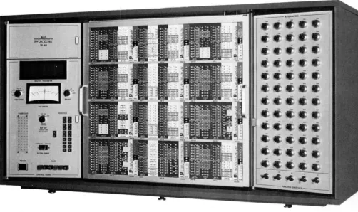
The PACE@> TR-48 (Figure 2.1-1) is a fully transistorized, general purpose analog computer.. Consisting entirely of solid-state circuit elements, the TR-48 is com-pact in size and is suitable for desk top mounting.. The computer is able to operate stably and accurately in normal office ambient conditions; there is no need for large primary po~r systems or special cooling duct installations since the po~r requirements are smallo Reliable, 'With simplicity in funct,ional design, the TR-48 is easy to use and can be a po-werful aid to the individual engineer in the rapid solution of scientific and engineering problems ..
The TR-48 utilizes a building block concept.9 in -which individual computing compon-ents may be easily interconnected to solve the required equations by forming elec-trical models analogous to the system tmder study. Each building block, either individually or in combination ~ith others, is capable of performing one or more of the follo-wing operations on variable DC voltages: mu.ltiplication by a constant, algebraic-summation, integration with respect to time, multiplication of t-wo vari-a.bles, and generation of kno-wn functions of a variable.. Each component has input and output terminations which are readily accessible at the computer Pre-Patch Panel for interconnection by bottle plugs (jumpers) and patch cords.
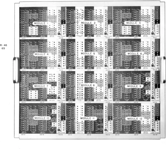
The Pre-Patch Panel is arranged in a series of t-welve similar modules, "With each module terminating a complete set of computing components • (Figure 2.1-2.) The modular design tends to eliminate patch-panel clutter caused by long across-the-panel patching. In addition, problem patching, checking, and trouble-shooting are more rea.dily accomplished, and patching errOl'S are less likelyo The five patching areas 'Within each module are color coded in vivid contrasting colors 'With large, clear lettering to help in faster and surer patchingo The PPatch Panel is re-movable to permit problem storage and also problem patching ~ithout committing operating time 0
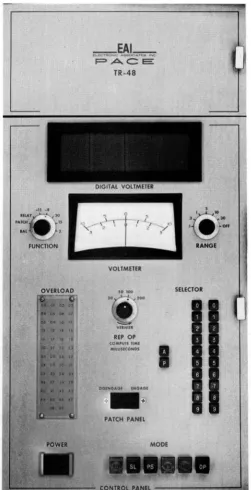
To the left of the Pre-Patch Panel is the monitoring and. control panel. This area contains the control s'Witches-~ and metering circuits 'Which permit turlling the com-puter on and off, engaging and dis-engaging the removable Pre-Patch Panel, and con-trolling the computer modeo Monitorir~ facilities consist of a digital voltmeter
and a multi-range voltmeter. The di.JSit.al. voltmeter permits setting problem para-meters to t-wo-deciroal accuracy and observing or measuring all comptttationaI and. operating potentials 0
To the right of the Pre-Patch Panel is the coefficient=-setting potentiometer and function switch panel. This panel provides space for a 1D.aXiro.um of sixty potentio"'"' meters and five function s-witches" Foux of every five potentj~ometers have one
end grounded while the fifth patezrtioJDeter is UXlgrot.m.dedo The potentiometers and .function switch connectiol'lS are ter.m1nated in the appropriate areas as indicated on the Pre-Patch Panelo
20 OPERATIBG COllSlDERAXIONS
The
TR-48
is shipped complete 'With all comPonents in place 0 The unit· is completelycalibrated and adjusted at the time of J:DBJl.uf'acture. A:rter performing the simple installation checkout procedure outlined in the mailltenance .m.anual, and connecting the unit to a suitable power source, the computer is rea~ for operation.
The use of low level reference supplies (+10 and -10 VOlts) 'With their associated curreJXt-limit1ng circuits eliminates shock hazards 'When patching 'With. the Pre-Patch Panel in place in. the computer 0 The current-limiting cirouits also protect
the reference supplies trom. damage due to shorting to groWld, or to each other. Thus an errm patohiitg connection (shorting the plus ref'erenoe to the minus
ref'-erence f'or example) 'Will not adverse.Q- ef'tect the supplies (output current drops to zero) nor 'Will the ref'erence supply tuses blo'Wo In addition, the .metal portiollS of the Pre-Patch Panel (except the handles) have a scratch-resistant, non-conduc-tive paixrt coating which, in conjunction 'With the plaStic patchillg blocks,
i!t-a~i-c.!Jl..Y eliminates shorting-out hanging patch cords.
/1/0
I
J 0. 0 < 1
,A. Preliminary Operating Considerations
The f'01l0lil1ng steps are recommended prior to operating the TR-48 to prevent possi-ble talse troupossi-ble indications 0
( 1) Ascertain that
.il.la
operational. amplifiers have ~-connectorbottle-plugs properly placed and seated as shown in Figure 2.2-1. This provides the ampli-fiers \lith feedback and preveJXts them. from overloading during the problem solution. The procedure for inserting and re.ID.Qving the Pre-Patch Pal'lel is described in
Sub-Paragraph .Q~
(2) . Patch the Digital Voltmeter (DVM) and .multi-range voltmeter (VM) to the selector readout system. (See Figure 2 • .3-2 and Paragraph
.3,&.
of this sectiontor
a deseription of' the selector system operation.)(.3 )
Apply power to the cOlllpu:ter and depress the .PS (potset) button. lni-tal.ly the overload lamps of the operational amplifiers will light; atter (l fewseconds all of the lamps sAould extinguisl1.
(4) Check the various supply' voltages of the TR-48. All power supply outputs are connected directly to the voltmeter FlDlClIOIIswitch (through appro-priate scaling resistors
1;
thus, the check may be accomplished simpJ.7 and rapidly.(See Paragraph .%,. of this s e c t i o n o ) ' '
( 5) Check the plus and .minus reference supplied
tor
readout on the DVM by selecting A49 and ~50o (See Paragraph 3A.)4
TR48
#45
A4642
[image:15.623.86.588.248.546.2]TR-48
[image:16.612.43.589.160.649.2];; 69
FIGURE 2.1-2
A4641
TR48
# 47)38
A4660
\
4 - (;CHNECTOR
BOTTLE·· PLUG ---.
. FIGURE 2.2-1 AMPLIFIER WITH FOUR-CONNECTOR BOTTLE-PLUG PROVIDING FEEDBACK
CAW ION
If' the VM FUNC'fIOB switch is in the PATCH position the selected voltages are also applied to the VMo Be sure the R.ANGE
s~itch is set to a high enough range
selec-tion to handle these input.s 0
(6) Allow a few .minutes war.m.-up time; this assures that the computing components, (including the DVM) are up to nor.mal. operating temperaturee Ground the DVM input termination (designated DVM on the 120763 READOU'l' PANEL) and adjust the DVM zero coxrt.rol on the back of the Control Panel door ( Figure 202-2) for a 00000 reading. Should the polarity relq begin to chatter, turn the zero control slightly clockwise until the chatter stops and the indicators retain the 00.00 display 0 The DVM zero adjustmem, should be checked daily; initia.lly, due to aging
of the precision components, this adjustment may be required more frequently.
(7) In the pat-set mode or the computer (PS button on the Comrol Panel depressed), closed relay contacts provide a feedback circuit
tor
the operational amplifier 0 (See Paragraph4
of this sectiontor
a more detailed deseriptiono)This teature permits the removal of the Pre-Patch Panel to balance the operational amplifier. However, when the computer is switched from. pot-set to a.lf1' other mode, the relay contacts open and the circuit as patched on the Pre-Patch Panel provides the feedback loop. Momentary amplitier overload may resu1t during the relay oper-ating time; thus to eliminate possible error in the com.p~er solu:t.ion, the operator should always switch the computer to re-set (depress the RS button) before switch-ing t~ the operate .mode 0 This permits the pat set relays to open and the
ampli-fier summing junctiOllS to settle before starting the problem solution. There is no act ual )fait1 V period required
a
that is, the operatormay
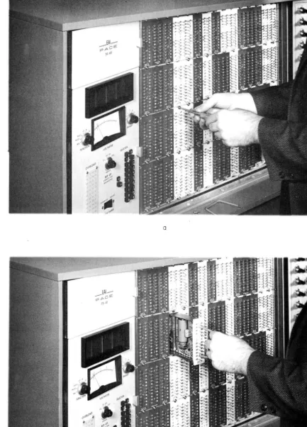
depress the RS button and then immediatelJr depress the button for the desired mode,. This sequence of operation will preveJIt the possible momentary- overloads .from effecting the proble.m solution •.Qo Pre-Patch Pan.el Insertion and Removal
To insert the Pre-Patch Panel, set the lip on the lower edge of the panel in the guide groove (Figure 2.2-3) 0 Push the top of the panel in so the pallel is
verti-cal. (A micro-switch will not pel'.mit the Pre-Patch Panel motor to function un-less the panel is properly seated.) Applying a slight hand pressure to the cen-ter of the panel (to maintain the panel in the vertical position) depress and hold the ENGAGE button on the Control Panel. (The com.puter must be in the pot-set mode 0) This button properly seats and firmJ.;y holds the Pre-Patch Panel in
position. Note that the ENGAGE and DISENGAGE positions of the switch are sprillg loaded; therefore, the switch
.must
be depressed and ~ lll'Jtil the l.1mit switches stop the motor operationo This feature eliminates the possibility of accident-a.lly engaging or disengaging the Pre-Patch Panel.hand pressure should again be placed on the panel to el1.m.1nate the possibility of
the panel falling forward when diseXlgsgedo
'£0 Amplifier Balance
The d-c operational. am.plif'iers are chopper stabilized to prevent drift and resultant errors in the computer results 0 Dritt in an amplifier results in an output voltage
(or 9J:~i'> with a zero inputo To el:\mjnate offset, the ampli.fiers of the
TR-48
) are b,alangeg, 10801 with a zero input, a b1as current is applied to the amplifierSWDm.ing junction equal and opposite to ~ current due to drift thus placing the sum.m:1.ng junction at virtual groundo Once balanced, drift in the am.pl:1.fiers is eliminated automatiea1.ly by the stabilizer circuit 0
The d~c amplifiers
or
the TR-48 are ,extremely stable and normally do not requirebalancing for periods up to several months 0 To asBure accuracy and confidence in the computer results, it J!J1J.Y be desirable to check the amplif'ier balance d.aily; this check can be made rapidly and simply sinee the selector system and voltmeter are usedo The following is a step by step procedure for checking amplifier balance 0
(1) Place the voltmeter FUNCTION switch in the BAL position and depress
the PS push .... button of the MODE s'Witcho
-(2) Using the selector system, select each amplifier AOO through A49 (A48 and
A49-
are the. plus reference and minus reference amplifiers respecti vely) 0 Thevoltmeter should register a zero deflection for each amplitierQ
(3) Should an amplifier cause a deflection to either side of the cemer .zero on the voltmeter, adj ust the corresponding balance control Q The balance con-trols for amplifiers AOO through A47 (the operational amplifiers) are located
di-rectly behind the Precopatch Panel (Figure 202<=348.) 0 The balance controls for
A48
and A49 (reference amplifiers) are located on the Reference Regulator 430104 be-hind the Potentiometer Panel (Figure 202<=4b) 0 Adjust t,hese controls for a zero
reading on the ~tero
,go
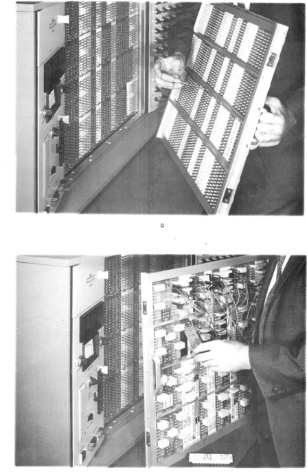
Changing Computational ComponentsIn the solution of some problems it may be necessary to add a specific type of co.mputational component to the existing com.plement Q Since ma.n;y of the .module po-sitions are designed to handle .more than one type of computing component, a com-ponent not required in the problem investigation may be removed and another unit
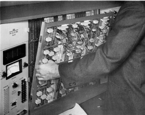
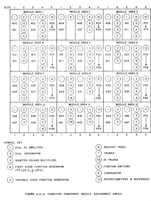
placed in that cradle 0 Figure 202-5 illustrates the various positions of the CO.DF
puting components in the TR-48 module areao Tb:is diagram illustrates 'Which type of computing component is com.patible with each cradle or .module positiono The procedure for replacing a computer component and changing the Pre .... Patch Panel patching block 1s described in the following Sub-Paragraphs (1) and (2) 0
TR48
#49
DVM ZERO
ADJUSTMENT
26.195 DVM
REACOUT
A4640
FIGURE 2.2-2. DVM ZERO ADJUSTMENT LOCATION
TR48 tt22
A4628
[image:21.614.84.579.205.599.2]TR-48 4 bf',67
A4656
DUAL INT
NET 12.764
'f ~ 4-~ .
•
•
~•
•
~,
.,
•
~•
•
::l.1.1.1.1.1.1.1.
• •POWER SUPPLY 10.203
-8V
1.5 AMP
+2V
.5 AMP
~---
-•
•
•
•
•
•
•
•
TIMING UN" b.1
0
.
.. i'
.~
.
.6' . ~.
,
•
.~,;
,
•
.:\,)FIGIJRE 2.2-4. AMPLIFIER BALANCE CONTROL LOCATION
AMPLIFIER BALANCE CONTROLS RF.:F:::P.ENCE AMF-LIrIER BAL.I\~JCE
A4643
SLOT 2 3 4 5 2 3 4 5 2 3 4 5
MODULE AREA I MODULE AREA 2 MODULE AREA 3
0
000
G
0
0
8 00 808 0
0
AOO
0
A020
poo A04 A060
P05 Aoa·0
AIO0
PIO+
~
+
AOI
0
A030
P04 A05 A070
P09 A098
All0
PI4'8
01
0
CD
...-MODULE AREA 4 MODULE AREA 5 MODULE AREA 6
MODULE AREA 7 MODULE AREA a MODULE AREA 9
P40
1
81010010808101080180
A24
0
A260
I P30 A2a8
A300)'
P35 A320
A340
A25
8
A278
I1
A29~
A310
I
1
A338
A350
P44
) 8
[01
P34~
I
P390
G)
~._. _M"--_--"--_.... _.. . .. ---L.. _ _ +-__ -..L _ _ _ . . . L . . _ - - i L - . _ _ --&..._----t
MODULE AREA 10 MODULE AREA II MODULE AREA 12
8
0)
810lG
(0
0
(0 0)
G 810 8 0
A36
0
A38 I0
P45 A400
A420
P50 A44 11
0
A460
A37
8
I
A 3 9 1 01
A41@
A438
1
A458
A478
I
G)
P49 P54CD
SYM BOL
8
(0
0)
8
2 3 4 5
KEY
DUAL DC AMPLI FIER
DUAL INTEGRATOR
QUARTER- SQUARE MULTIPLIER
FIXED DIODE FUNCTION GENERATOR
(X2, LOG X',
t
LOG X )2 3 4 5 2 3 4
0
READOUT PANEL(2)
TRUNKS@
IN TRUNKS0
FUNCTION SWITCHESCD
COMPARATORP55
1
P59
5
VARIABLE DIODE FUNCTION GENERATOR
G
POTENTIOMETERS 81 REFERENCE [image:23.617.41.569.40.744.2]NOXE
Failure to change the Pre .... Patch Panel patch.ing block: may prevent proper use of a computer co~onent due to the arrtmge.ment of jumpers on the rear
ot
the patching blocko
( 1 ) CQP1Ruti Qi Module [email protected]
(.&) Remove the Prec::oopatch Panel to expose the compone:n:t modules 0
Re-move the t'Wo ph:1.llips .... head rets.:i ning screws from the top and bot-tom of the module to be reJJlOVed (Figure 202 -6) 0
(.b) Insert the special module removal handle in the holes provided
in the central area of the lIlOdule (Figure 202-6) 0 Pull the module
forward removing it £'rom the
TR-48o
(.Q.) Place the nell component in place, be sure the guide pins are
pro-perly seated in the guide=>pin holes before mating the connectors at the rear of the moduleo
(J1) Check that the m.odule is properly installed (connector fir.rnly .mated, etc 0) and replace the
two
retaini ng screws 0(2) Patching Block Replacement
(II) The Patching blocks
or
the computing componen:ts are held securely in place by the retaining strips on the trontot
the Pre-Patch Panel (Figure 202-78,) 0(li.) ~he retainiDg strip above or belo'W the patching block JDJq be
re.m.oved to change blocks 0 The retaining strip is released by
removing the four screws directly behind th~ strip on the rear of the Pre-Patch Panel (Figure 202-7b) 0
t;,) Once the retainiDg strip is free, remove the original patching block and replace it with the DeW block (Figure 202=>7) 0 Secure
the retainiDg strip with the four screws 0 The Pre--Patch Panel
is now ready for problem patchingo
NOTE
I f blocks on two adjaoent horizontal rOlls
are to be replaced it is onlJr necess8rJ" to remove the retaini.ng strip between the two rows 0 Patching blooks IDB.y then be re.m.oved
from the row above and below the stripo
3. MONITORING AND COB'l'ROL
The control panel of the TR-48 is designed to allow simple control and monitoring of the computer components (Figure 2 • .3-1) 0 The following sub-paragraph describes
the function and operation of the various switches and coIXtrols mounted on this panel 0
1!. Signal Selector
The signal selector consists of three vertical rows of pushbuttons; The first row contains two buttons designated A and P, and the second (tens) and third (units) ro'Ws contain buttoDS designated 0 through 9. DepressiDg the A button permits the
operator to select the outputs of the
48
operational amplifiers (ADO through A47), the two reference supply amplifiersA48
and A49 (plus and .minus reference respec-tively), and 15 of the Ili trunk lines (selected as A50 through A64) 0 Depressing theP button permits the operator to select the individual wiper outputs or the sixty potentiometers (POD through P59).
Depressing the tens button (assum.ing the A button is depressed) sets the selector system for amplifiers in a given tens group, i.e., if the 2 button in the tens ro'W is depressed, amplifiers A20 through A29 are set up for selection. The units but-ton deter.m.iDes which of these ten amplifiers is actually selected. The selector system button numbering corresponds with the amplifier and potentiometer designa-tions as .marked on the Pre-Patch Panel and Potentiometer Panel respeoti vely.
Once the letter and tellS seleotor buttons are depressed, say P1 (addressing P10 through P19), the individual potemiometers of this group may be seleoted by merely changing the units designation button, i.e., if P10 is selected, P11 .IDS\Y
be selected by depressillg the units 1 button only.
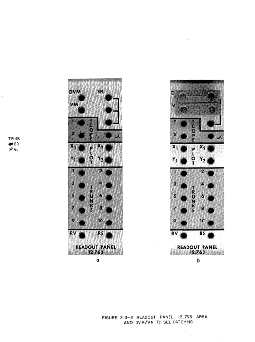
The selector system output is connected to the three terminations .marked SEL in
the upper white portion of the 12.763 Readout Panel (Figure 2 • .3-2a).
In order to read out a selected signal on the DVM, the upper bottle plug show in Figure 2 • .3-2b must be in place. The multi-range voltmeter (VM) may also be con-nected to the selector liDe by installing the lO'Wer bottle plug show. in the illus-tration (the VM FUNCTION s'Witch must be in the PATCH position). It should be noted, however, that the VM circuit 'Will load the output of the selected component with a relatively low impedance and should not be used if the monitored circuits oannot tolerate this load. (Set the FUNCTION switch to a position other than P MCH to disconnect the VM from the SEL terminations.) The YX shottld not be used when
set-tiDi attenuators. To prevent this possibility from accidently occurrillg, a relay
cirouit disconnects the VM from the selector system when the com.puter is \placed in the pot-set mode •
.b..
Digital VoltmeterThe Transistorized Digital Voltmeter 260183 is terminated in the 12.763 Readout Panel area (Figure 20.3-28) and is designated DVM. As previously mentioned the
TR 48 #26 #29
FIGURE 2.2-6
A4654
a
b
[image:26.618.112.546.70.673.2]TR48
# 23 # 24
A4658
a
b
[image:27.615.99.546.49.735.2]TR48
# 48
A4644
P A C e : :
TR-48
VOLTMETER
so Joo
REP OP
(O",,'UJf liME MIlUS(CONDS
0151N0401 (NOAOt PATCH PANEL
SELECTOR
I
[image:28.614.226.478.123.614.2]TR48
#60
#61
a
A4655
READOUT PANEL i.~t:,~:~l~l\~:;}5;/~~ ~;} ;:;~~.~ lli~«t'
..
·:i;'~~~L~~iC~~:~~i$lj~~~:b
FIGURE 2.3-2 READOUT PANEL 12.763 AREA
[image:29.615.41.566.55.759.2]DVM may be bottled to the SEL termination to monitor the seleetor system voltages, or "With a patch cord the DVM may be used to monitor signal levels at practically
arv
termination in the Pre-Patch Panel 0 The DVM has a 10 .megohm (minimum)full-time input impedance.
h
r
-the
J7
VM
The only operational setting requiredjlis periodic adjustment of the zero control. (See Paragraph ~o, Operating Considerationso)
,£0 Multi-Range Voltmeter
The Multi-Range Voltmeter is permanently wired into various circuits of the TR-48 to facilitate rapid readout of certain voltages by selectd.on with the meter
FUNC-TION switch. The voltmeter also has a RANGE switch, thus permitting close to full scale readouts for maximum. accuracyo The ranges are 001, 00.3, 1, .3, 10, and
.30
volts, (in addition to an off position) 0 The RANGE switch functions only when thefunction switch is in the PATCH position.. The PATCH p<)"'sition connects the volt-.meter to the Pre-Patch Panel VM ter.m:ination (Figure 20.3--2) permitting this point to be bottle-plugged to the SEL output or, as in the case of the DVM, monitoring voltages at most Pre-Patch Panel terminations via a patch cordo
FolloYJing is a list of the voltmeter FUNCTION s1Jitch positions 'With a brief des-cription of the function of each position.
POSITIO;
BAL
PATCH
RELAY
-15, -8, 30, 15,
and 2So
Computer MODEDESCRlrrION
Connects the stabilizer output of the amplifier addressed by the selector system to the meter to facilitate checking and/or adjusting the amplifier balanceo
Connects the .meter, via the RANGE switch, to the
VM Pre-Patch Panel terminationo
Connects meter to the relay powr supply (-20 volts) 0
Connects voltmeter to output of corresponding
power supplyo ~ ~~~
a..e2f2<k
~.~~,
The operating mode of the computer is controlled by the six-pushbutton selector just to the right of the POWER button (Figure 20.3-1) 0 Follo'Wing is a list of the
pushbutton and 'brief description of their functioDSo
mDE
13ur:rONOP (Operate)
DESCRIP!rON
When this pushbutton is depressed, all integra-tors are simultaneously released to respond to
MODE Bl11'%QJi
OP (Operate) (Continued)
HD (Hold)
RS (Reset)
PS (Pot Set)
SL (Slave)
RO (Rep-Op)
.I.e Overload Indicators
DESCRIPlION
input signal voltageso The integrator outputs change in potential as dictated by the inputs; a time vary-illg behavior is producedo This generates the voltage solution of the programmed problemo
Depressing the HD pushbutton permits the problem solu-tion to be stopped and all voltages held at the poten-tial attained up to the instant of depressing the but-tono The problem J.TJay be continued from. this point by depressing the OP button or re-set to the starting point by depressing the RS buttono
In the RESE:! mode all circuits except the integrators function normallyo The integrator outputs are held at their respective initial conditions (IC) as dic-tated by the IC input voltage 0 (The integrator
out-put is zero if no IC voltage is appliedo)
Amplifier input resistor summing junction grounded; permts setting potentiometers under actual loado Al-so provides amplifiers with relay-contact feedback Al-so Patch Panel may be removed to balance amplifierso
When a TR-48 Computer is to be slaved to another TR-48 (master) this button is depressedo The slaved computer then responds to the selected modes of the master
C01l1-puter pushbuttons 0
The RO button switches the computer into the repetitive operation mode 0 The computer switches automatically
between operate and reset at a predetermined rate 0
(See Paragraph ~ of this sectiono)
~
The overload indicators (Figure 20.3-1) provide a visual aJ..sxm when an overload oc-curs in a:IJ.y of the operational amplifiers, 1oeo, 'When the summing junction is not
at virtual grounde An overload IDB.y be due to improper scaling, improper patching . or . loading ~
When the computer is initially turned on, all the indicator lamps may light,; however, in a few seconds, as the amplifiers settle, all the lamps should go out 0 Should a
lamp remain lit it cou.l.d be caused by a patching error such as the failure to
pro-vide un-used amplifiers 'With feedback (via the four connect or bottle plugs) 0
Pro-longed overloads 'Will not damage an amplifiero
I..
TrunksThe trunks (terminating at the Trunk 12.762 area) provide point-to-point connections to the connectors at the left ... rear of the computer (Figure 2.3-3). These connectors may be used as outputs to accessory equipment, or the trunk terminations may be cabled to a second TR-48 as signal carrying lines for the interconnection of the problems patched on the separate Pre-Patch Panels of slaved computers.
£,. Readout Devices
The problem solution obtained from the TR-48 r:ru:r:y be permanently recorded or tempor-arily displayed on various types of readout devices. A fe'W of the more common read-' out devices are described in this paragraph.
Either the DVM or voltmeter may be used to read out the problem solution. These devices, hO'Wever, do not record the solution and thus a permanent record is not made. When in REP-oP the computer solution is, continuously displayed on an oscillo-scope; in this case a permanent record IDB.y be obtained by photographing the scope trace. X-I plotters (such as the EAI 1110 VARIPLO'I'TER@) or strip-chart recorders may be used for a permanent record of TR-48 problem solutions. These units, hOll-ever, do not have the frequency response necessary to accurately record the solution 'When the computer is placed in the high-speed REP-oP mode of operation. The Readout Panel scope and plotter terminations are 'Wired to connector plugs at the rear of the TR-48. See Figure 2.3-3.
4.
ATTENU,ATORSOne of the simplest and most useful operations performed on an analog computer is
the multiplication of a variable voltage by a positive constant less than unity; ioe
0,
attenuation of a signal.. The TR-48 has a basic complement of 10 attenuators (or pot,entiometers) androay be expanded to a full complement of 60 potentio.meters.Each Attenuator Group 420283 provides five potentiometers far setting problem co-efficients, initial conditions, and problem inputs. The potentiometers are mounted in up to 12 horizontal ro'Ws of five potentiometers per ro'Wo Each rOll is terminated
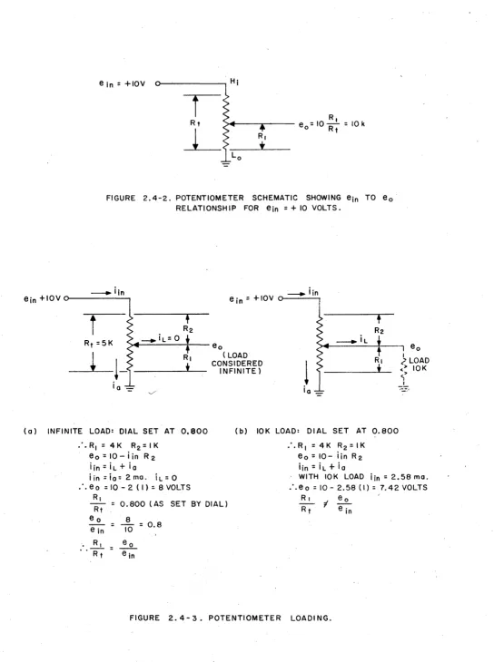
at an individual patching area of the Pre"'"Patch Panel; space is provided for one potentiometer patching area per module of the Pre-Patch Panel 0 Four of thefi ve
potentiometers have one end grounded 'While the fifth has both ends ungrounded. (See Figure 204-10)
~'he standard potentiometers in the TR .... 48 are 10 turn, 'Wire 'Wound , 5000 ohms,
individ-ually fused. units 'With calibrated dials and a~-rocking mechanismo
The potentiometer may be used in conj unction 'With reference to obtain a fixed lIaccura'te voltage less than reference, or to mUltiply a problem variable b
con-stant less than unity. Figure 204 .... 2 is a schema: l.e 0 a potentiometer 'With +10
volts applied to the high end*; the output at the 'Wiper is k times +10, where k is:
&
k
=:1
&.r
(EQ.
2.4-1)The potentiometer shown in Figure 2.4-2 is unloaded, and the .mechanical ratio of R1
:1iT
equals the electrical ratio eo:ein; thus, the potentiometer I1JJ3:y be set tothe exact ratio by .means of the calibrated dial attached to the 'Wiper shaft. How-ever, the t'Wo ratios will not be equal when the potentiometer is loaded as is the case when it is used as a computer problem. element 0 ~or.mally, the pot is loaded
b 100,000 (100K) or 10,000 (10K) ohms resistor since a potentiometer gen-erall eeds an amplifier an ese values are e
moSt
-common amplifier inputre-~istors 0 Figure ustrates e e on the ein:eo and &1 :RT ratios 'When
the potentiometer 'Wiper feeds a 10K load.
In order to el1.minate the effects of loading, it is more convenient to set the
po-tentiometers under actuar-roaa- 8.1ld]noriit"-or--the wiper voltage (the potentiometer out-put), than to calculate a corre-eted .mechanical ratio (&1:liT).
Figure 2.4-4& and b illustrate the TR-48 circuitry provided to permit setting the potentiometers under actual load. Relay K1 is energized 'When the computer is placed in the pot set mode (depress PS button) and applies +10 volts reference to the Hi ends of all the grounded potentiom.eters 0 Note that the 'Wiper remains connected to
the Pre-Patch Panel termination; thus, the 'Wiper If sees n the impedance
ot
the actualload it is patched to in the problem. Even 'When the potentiometer is selected f'or monitoring via the readout system and 12 is energized, the 'Wiper remains coxmected to its actual load. The readout system connects the 'Wiper to a high impedance DVM
(10 megohms minimum) or, in the absence of' the
DVM,
a null pot circuit. The opera-tor ~ then set the 'Wipertor
the attenuation tactor required in the problem.The .method
ot
setting the u,ngrounded potentiometers is si.milar except the +10 volt reference is not automatically applied to the potentiometer high end (relay K1 is el1.minated on ungrounded attenuators). ~_:1.l~.~ rator must atch inputs to the0-telXtio.meter; this arrangement prevents possible erroneous settings depen on
R
ilie con1:'1iW:-atioll in which the potelXtiometer is used.
)IV!
f
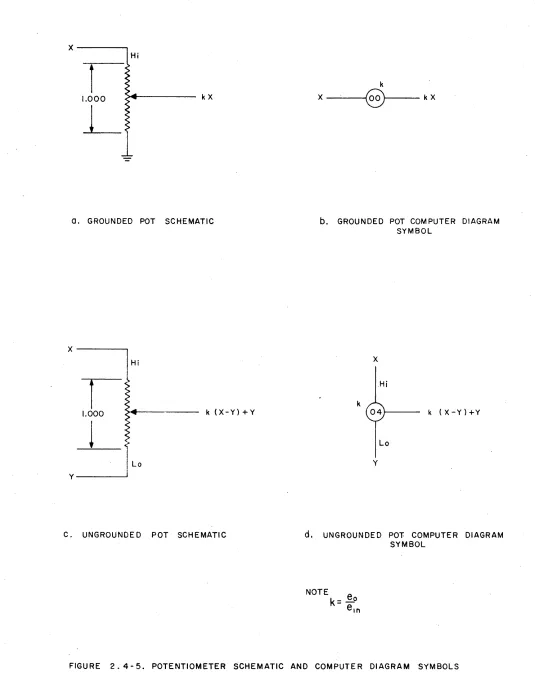
Figure 2.4-5 shows schematics and symbols for the
two
types of potentiometer con-figurations. The TR-48 potentiometer designation (i .• e., nwn1?er) is given within the circular symbol and the setting is witten in close proximity to the symbol.In addition, the Hi and Lo ends of the ungrounded potentiometer(s) are also desig-nated to indicate clearly both input signal sources.
*The high (or hi) end of a potentiometer refers to the- termination physically loca-ted at the top of the schematic designation of the Pre-Patch Panel. The low (or 10) end is the bottom. termination, nor.mally grounded except' in the case
ot
theun-grounded potentio.mter.
TR48 #68
A4629
TR 48
#56
-# 37
AlTEN
A4657
, - - - -- - - - POTENTIOMETERS - - - -- - ,
'01
';I'
'3\ '31
•
•
42.283
51 52 53 5' ss FUNCTION SWITCHES - - - '
FIGURE 2.4 - I ATTENUATOR GROUP 42.283
A4645
e in = +IOV
I
R,R t ~"---..---- e = 10 - = 10 k
[image:36.613.56.600.38.768.2]L O R I
FIGURE 2.4-2. POTENTIOMETER SCHEMATIC SHOWING ein TO eo
RELATIONSH IP FOR ein = + 10 VOLTS.
---+ iin
e in + 10V 0 - - - . e in = +IOV 0 -+iin I
i
Rt = 5K
*
+
R2
- + iL
=
0~I---++---eo
RI (LOAD
+
CONSIDERED- INFINITE)
---+ iL
!
ia _eo
?
LOAD<> 10K
<,> -!....
(0) INFINITE LOAD: DIAL SET AT 0,800 (b) 10K LOAD: DIAL SET AT 0.800
o·.R1=4K R2=IK
eo = 10 - i in R 2
iin=iL+ ia
iin=i a=2mo. iL=O
•.. eo = 10 - 2 ( I) = 8 VOLTS RI
Rt
= 0.800 (AS SET BY DIAL)eo 8
- - = -10 = 0.8
ein
• R, = ~
. 'Rt
eln: . R I = 4 K R2 = I K
eo
=
10- iin R2iin=iL+ia
WITH 10K LOAD iin = 2.58 mo .
:.eo = 10 - 2.58 (I) = 7.42 VOLTS
R,
Rt
'TO PRE- PATCH PANEL Hi TERMINATION
TO +IOV REF.
TO PRE-PATCH PANEL Hi TERMINATION
TO PRE-PATCH PANEL Lo TERMINATION
A4646
~...--I
----.,I I
~/ Hi
j
P.s (f'~f sei)
/#z;de
Lo
K2
a. GROUNDED POTENTIOMETER CIRCUIT
Hi
r----.
I ---0----+
b--A
K2b. UNGROUNDED POTENTIOMETER CI RCUIT
TO WIPER PRE-PATCH PANEL TERM INATION
TO READOUT SELECTOR
SYSTEM
I/O
VTO WIPER PRE-PATCH PANEL TERMINATION
TO POT SELECTOR
SYSTEM
A4647
a. GROUNDED POT SCHEMATIC
X
1Hi
I '
I.r
1---··-to
k <X-Y) +Y
Y - - - _ - I1
C. UNGROUNDE D POT SCHEMATIC
b. GROUNDED POT COMPUTER DIAGRAM
SYMBOL
x
.Hi
k
0 4 1 - - - - k (X-Y)+Y
Lo
y
d. UNGROUNDED POT COMPUTER DIAGRAM
[image:38.612.50.585.52.728.2]SYMBOL
5.
OPERAtIONAL AMPLIFIER.&. General Considerations
Vlhen a hlgh-gain d-c amplifier is used in conjunction with input and feedback networks to perfor.m mathematical. operations, the resulting system. is generally referred to as an operational amplifier. The operational amplifier is the basic and .most versatile unit in the analog computer 0 It can be used for inversion,
summation, .multiplication by a constant, integration, and used in conjunction with special networks for squaring, extracting square root, generatiDg logarithmic functions, etc 0
To understand the basic concept of the operational amplifier, consider the si.mpli-fied block diagram of Figure 205-1 'Where a high-gain amplifier (gain of -A) has a feedback impedance Zt and an input i.mpedance Zin. The amplifier is designed so that it has three basic and essential characteristics.
(1) The amplifier output (eo) is related to the summing junct~on voltage (eb) by the gain of the amplifierg eo = -Aeb
(2) The input stage of the amplifier draws negligible current; 1b :: 0
(3) The open loop gain of the amplifier is extremely high! ~ (on the order of
3 :x
107 at d-c).UsiDg Kirchhoff's lalls, the nodal curreJXt eqll8.tion at the summiDg junction (SJ) is:
or
(EQ.
2.5-1)since eb =
-eo/A,
and since ib=
0 , Equation 2.;-1can
be re'WZ'itten to obtain:Solving for eo:
ein eo eo eo
-+-=----Zin AZin AZf Zr
e • o
- if;
ain(EQ.
2.;"2)In m.ost applications the ratio of Zf to Zin is less than 30 and since 1/ A approaches zero Equation 2.5-2 becomes:
eo
=-{::~
e1n
(EQ. 2.5-3)
Equation 2.5-3 illustrates one of the m.ost im.portant considerations Of the operational amplifier: The input-output telationship of the gperational amplifier is solely de-pendent, on the ratio
at
the feedback to the input i;wdApce.Using Equation 2.5-3 as the basis of discussion, the following sub-paragraphs des-cribe the various uses of the operational amplifier.
( 1) InyersioA. When the same value resistor is used for both the feedback and the input impedance, the amplifier output voltage has the same amplitude as the in-put voltage but is opposite in polarity.
Rf
eo = - - ein
R
inIn the TR-48 the value of lif and Rin used for the inverter is nor.m.ally 100,000 ohms, (100K) therefore:
100K
eo == - - ein == -ein 100K
Thus a +10 volt input results in a -10 volt output, and the amplifier is said to have a gain of minus one. The accuracy of the output to input ratio depends solely on the accuracy of the ratio Rf/Rin.
(2) Multiplication by a Cgn§tgnt. A change in the ratio of the resistors re-sults in multiplication by a constant. With lif equal to 100K and Rin equal to 10K, for example, the amplifier output is:
eo = -
~
ein = -10ein 10KAn input of plus one volt results in an output of minus ten volts. This operational amplifier has a gain of ten. The multiplying constant can be made smaller than one by using a 10K feedback resistor with a 100K input resistor.
e
= -
1Q!L
ein=
-o.
1eino 100K
An input of minus ten volts produces an output of plus one volt.
(3) Summation. When multiple input resistors are used with a feedback resistor Rf , the basic relationship is extended to:
A4648
I f
--~ .---~ Z f \---- I
r - - - , i i n S J
T1
l i nI
-r
r
L
b. PATCHING BLOCK
A4633
SJ
~--~~----.-~()
I
I I I
~~O
POT SET
r--_
.
RELAY ~
RELAY VOLTS POT SET BUS
o. SIMPLIFIED SCHEMATIC OF 1/2 OF THE
DUAL DC AMPLIFIER
FIGURE 2. 5-2. TR~48 OPERATIONAL AMPLIFIER I SIMPLIFIED SCHEMATIC
(0)
A4634
XI - - - I
X2--...,.I---I
10
X3 --~--1
10
X4 - - - - I
(c)
The circuit can be used to algebraically sum an indefinite number of inputs; further-more, each input may be multiplied by an arb.i trary consta.nt 0
(4) Integration with Respect to Xi
me
0 When the feedback element Zf is acapacitor rather than a resistor, the summing junction current equation is:
000
Integrating th~s equation and assuming an initial charge on the feedback capacitor of Vo~
Lookini at this another ~ay, i f Zf is a capacitor having an operational impedance 1/pC and Zin is a reSistor, the basic operational amplifier relationship, Equation 205-3, becomes:
E t
e = - : i n = - L S o e . dt
o pRC RC ~n
'With this arrangement, the operational amplifier 'Will integrate (with respect to
time) any input voltageo In. addition to integrati.ng, the amplifier also inverts the input voltageo An indefinite number of inputs may be applied to produce the time-integral of the sum of the input voltages 0
(5) other Mathematical Operationso As previously indicated the operational amplifier has uses other than those indicated in sub-paragraph!! through
go
COJIl-plicated transfer functions can be simulated by using series and parallelRC net-'Works for the feedback and input impedances 0 The circuit performance is still
governed by the basic relationship of Equation 205-20 For the general case 'Where three-terminal net'Works are used, the short-circui.t transfer impedance of Zr andZin
IllUSt be usedo (The short circuit transfer impedance of a network is the ratio of input voltage to short-circuit output current 0) The input and feedback elements need not be linear; therefore, almost any non-linear characteristic can be approxi-mated 0 The amplifier can also be used in conjunction ~ith diodes and resistors to
simulate the non-linear operations of limiting, de~d-zone generation, X2, Log X, etco
.Qo
TR-48
Operational Amplifier 60514Figure 205-2 shows the operational amplifier patching terminations and a simplified schematic of the high gain d .. c amplifier and summing resistor networko By placing a four-connector bottle plug in the patching block as shown in Figure 205-3a, the high-gain amplifier is connected to the summing resistor network as shown in Figure 205-3bo The resultant operational amplifier can be used for inversion, multiplica-tion by a constant, and summamultiplica-tion. The computer diagram symbol is shown in Figure 205-3c 0 On the computer diagram it is customary to show only those inputs that are used; the amplifier number is written inside the triangular symbol 0
Figure 2o',-4a sho'Ws the patching to provide an operational amplifier that is capable of integrating 'With respect to time 0 Figure 205-4b illustrates a siInplified sche-matic for an amplifier patched as an integrator <> The computer symbol for an
inte-grator is sho'Wn in Figure 205-4co
Figure 205""'5 is an expanded schematic of the integrator amplifier 0 In addition to the terminations interconnected by the Tee-shaped bottle plug, certain circuits are brought out to the patching block for additional control of the integrators. These incillde the Operate and Reset relay coils and the operate end reset buseso Normally these ter.minations are connected as shown in Figure 205-4; however, by cross patch-ing (operate bus to reset relay, etc.)' the integrator can be used as a track and
hold unit.
An additional featare is the 10~ terminations; for normal operation these t'Wo term-inations are jumpered by a t'Wo-connector bottle plug (Figur,e 205-4). This bottle plug parallels a 9 microfarad 'With a 1 microfarad capacitor (Figure 2.5-5) to
pro-duce an integrating rate of 10 VOlts/second for the gain-of-ten inputs and 1 volt/ second for the gain-of-one inputs., By removing tfie
10f3
bottle plug the integrating rate can be increased by, a factor of teno60 QU.ARTER.,."SQUARE MULTIPLIER.
Multiplication of tvo variables is one of the non-linear operations necessary in a general purpose computer 0 The TR-48 Multiplierlltilizes the quarter-square
multipli-cation technique to produce a product of tlllo variables (X and Y) as illustrated by the following equation:
. 1
Xy
= - [(X
+y)2 - (X - y)2J
4
The TR-48 Quarter-Square Multiplier is basically a gated-resistor circuit applica-tion of the quarter-square technique. When the quarter-square multiplier is used as the input impedance Zin for a high-gain d-c amplj.fier, the resultant circuit is capable of multiplication or squaring of input variables 0 When used as the feed-back impedance, the multiplier-amplifier combination is capable of division
or
ex-tracting the square root of the input variables. The quarter-square multiplier, A4635
TEE BOTTLE PLUG
a. PATCHING
2.-CONNECTOR BOTTLE PLUG
(10
f3
AREA)I
0
10
10
lOOK
lOOK
lOOK
10K
10K
10MFD
o
")---ja---10
b.' INTEGRATOR SIMPLIFIED SCHEMATIC
IC I
4-CONNECTOR BOTTLE PLUG
10 10
c. COMPUTER DIAGRAM SYMBOLS
NOTE:
IF AMPLIFIER IS NOT USED, BOTTLE PLUG REQUIRED TO PROVIDE FEEDBACK.
AMPLlFIE;-
=-:=J
RESISTOR NETWORK
I
10 lOOK I
I tOOK
Ol---...-J'o.t'\/\,....--...
SJ 'r\1 lOOK
10~~
10K , _IO~
ICIS
Ir __
~_INS~iEI
,,~ TO RESET BUS
I RESET (-20V NOM)
\
SJ
A4649
INTEGRATOR NETWORK
~
(@
@
@ I10K
~III-"""""'··"""'H
Y' ~-.. ~ .... ." ""
1QE),
d
i (!) I
I SEE
I
AMPLlFI_ERNOTE·
-4
RELAY K3 SHOWN
I
IN HOLD POSITIONo
\
I \
I
>--_ ... - I ° t /
@
SEE NOTE 4
, ()r---~---~---... ___
K2 K3
, Qr---... - - - - e . -... ---' I
I OPERATE
",t
__
T_O_O_PE_RATE BUS (-20V NOM)-I
--~
NOTES:
I. ONLY ONE OF TWO INTEGRATOR
NETWORKS SHOWN.
2. RELAYS K2 AND K3 COMMON TO BOTH NETWORKS OF 12.764.
3. REP-OP CAPACITORS AND
RE-LAYS ELIMINATED FOR
CLAR-1Ty. (SEE PARAGRAPH 8).
4. THESE THREE CONNECTIONS NORMALLY MADE BY TEE
BOTTLE PLU~
<D .
5. RELAYS SHOWN DE - ENERGIZED
A4650-1
R:38
CR7
R:37
RI7
-IOV R f
R:36 :3500
Xin
CR6
_[ 1/4(1:+y)2]
R:35 I
Yin
R23 I
I
I
-IOV I
I
I I I
R26 CRI I I
R25 RI8
-IOV
10
9
2 8
( X+V)
7
40
OUTPUT 6
5
4 3
2
o 2 4 6 8 10 12 14 16 18 20
( X +y) INPUT