DEC STO _ _ 1...,5_9 _ _ PAGE 1.0
TITLE: MASSBUS Specification
~HISTORY: The Massbus Interface concept was suggested by Gordon Bell In July, 1972. A conmlttee was formed of: Tom Hastings, Steve Jenkins, Vic Ku, John Levy, and Pete McLean, who defined the .Inte"rface through Its first several design Iterations. John Levy acted as secretary and published the followln, precursors to this document:
August 2, 1972, Standard Mass Storage Interface--Prellmlnary SpecificatIon
August 28, ·1972, Mass Storase Interface Standard October 16, 1972, Massbus Interface Standard
March 20, 1973, Massbus Interface Speclflcatlon--Part 1
These four documents are sometimes Informally referred to as "verslon 1", ,"version 2", "version
3",
and "verslon 4" of the Massbus Interfacespec 1 fl cat Ion •.
DATE 0 # AUTHOR ... ·"',.vED REV SEC PAGES TITLE
MASSBUS Secification
DEC STD 159
SIZE CODE NUMBER REV
A
os
EL00159 AEN-I047A-16-R27S-(327)
PAGE REVISION CONTROL
:p~~: REVISIONS PAGE
PAGE REVISIONS
PAGE NO.
1.0 A 19.0 A
2.0 A
20.0 A
3.0 A 21.0 A
4.0 IA 22.0 A
5.0 ~ 23.0 A
6.0 A 24.0 A.
7.0 A 25.0 A
8.0 A 26.0 A
9.0 A 27.0 A
10.0 A 28.0 A
11.0 A 29.0 A
12.0 A ~O.O A
13.0 A 31.0 A
t4.0 A 32.0 A
15.0 ·A ~3.0 A
16.0 A ~4.0 A
17.0 A ~5.0 A
18.0 A 35.5 A
ECO ECO
NO. NO.
DATE DATE
~~~. ~r~·
~t~ STD
REV
DEC STD
159REV
APAGE
3.0.
PAGE REVISION CONTRnL
rp~~: PAGE REVISIONS PAgE
NO. PAGE REVISIONS
36. ( A 54.0 A
37.( A 55.0 A
38.( A 56.0 A
39.( A 57.0 A
40.(J A 58.0 A
41.(J A 59.0 A
42.0 A 60.0 A
43.0 A ~1.0 A
44.0 A ~2.0 A
45.0 A ~3.0 A
46.0 A ~4.0 A
47.0 A ~4.5 A
48.0 A ~5.0 A
49.0 A p6.0 A
~O.O A p7.0 A
51.0 A ~8.0 A
52.0 A I
p9.0 A
53.0 A ~O. 0 A
ECO ECO
NO. NO.
DATE DATE
~~~. ~E~·
~f~ SlD R V
.
DEC F~R~NO.16-(327)-11 06-Nl75
PAGE REVISION CONTR~)L
rP~g: PAGE REVISIONS PAGE
PAGE REVISIONS NO.
71. ( A 89. ( A
72.( A 90.( A
73. ( A 91. ( A.
74. C A 92. ( A
~5.0 A 93.0 A
r76.0 A 94.0 A
'rJ7.0 A 95,Q A
78.0 A
79.0 A
80.0 A
Sl.O A
82.0 A
83.0 A
84.0 A
85.0 A
86.0 A
87.0 A
88.0 A
ECO ECO
NO. NO.
DATE DATE
~~~. ~~~.
~fS STD
REV
.
DEC STD
1.
159 REV A
CONTENTS INTRODUCTION
1.1 " Motivation
1.2" Goals of This Specification 1.3 Glossary
1.4 Flowchart notatIon
2. SUMMARY
PAGE 5.0
2.1 DIvision of Functions Between Controller and Drive
2.2 Configurations
2.3 Physical Constraints 2.4 General Abstract
3. THE CONTROL BUS
3.1 Introduction
3.2 Control Bus Signals
3.3 Sequence and TimIng of Control Bus Transfers 3.4 Command Initiation
3.5 The Attention Line (ATTN)
3.6 The Initialize Line (INIT)
3.7 Control Bus Parity Checking
3.8 Other Control Bus Timing Constraints
4~ THE DATA BUS
4.1 IntroductIon 4.2 Data Bus Signals
4.3 Sequence and Timing of Data Bus Transfers 4.4 Data Bus ParIty Checking
4.5 Error Signalling
4.6 Data Transfer Command Tennlnatlon
4.7 Additional Data Bus Timing Restrictions
4.8 Recommended Pulse Durations
5. DRIVE REGISTERS
5.1 Introduction
5.2 Description of Drive
Registers-5.3 Details of Mandatory Drive Registers
6. COMMANDS
6.1 Command Codes
6.2 Command Descriptions
7. ERROR CONDITIONS 7.1 Introduction
7.2 Use of AttentIon (ATTN) 7.3 Use of exceptIon (EXC)
7.4 Class A Error Handling Protocol 7.5 Class B Error Hand11nl Protocol 7.6 Examples of Class A Errors 7.7 Examples of Class B Errors
8. OPTIONS
8.1 Dual Controller 9. HARDWARE DESIGN NOTES
9.1 Introduction
9.2 Notes on Massbus Protocol
9.3 Notes on Massbus Tlmlnl
9.4 Notes on the Use of ATA (AttentIon Active) 10. PROGRAMMING NOTES
10.1 Introduction
10.2 General ImplIcatIons of the Massbus for Software 10.3 Programming Notes on Massbus Timing
10.4 Prograll'lnlng Notes on Massbus Conmands
10.5 Notes on the Attention Condition
11. ELECTRICAL SPECIFICATION 11.1 Introduction
11.2 Components
11.3 St.andard Transce Iver Modul es
11.4 Approved Massbus Hardware
mamaama
EN-OI047-1A-16-R175-(327)DEC STD 1. 1.0 1.0.0 1.1 1.1.0 1.1.1 1.1.2 1.1.3 1.2 1.2.1 1.2.2 1.2.3
159 REV A PAGE 7.0
I NTKUUU\; I I UN
GENERAL
This document specifies a standard Interface between
controller~ and mass-storage devices. It Is a company standard applied to disks, drums, tapes, and other magnetic or cyc'llc storaae media.
MOTIVATION
The following considerations motivated the ceneratlon of a standard Interface.
The existing number of combinations of controllers and devices Is too large. Past practice was to design and buIld a new controller for each perIpheral device. Standardization allows constructIon of controllers whIch handle more than one drIve In a serIes (e.g., RP04, RPOS, ••• ) and more than one type of drive (e.g., RK and RS disks). Controllers with such compatibility not only have a longer market life, but also give more flexibility to the customer.
A great deal of "re-Inventlng the wheel" takes place each time a new controller Is designed. A standard Interface specification provides a basis for desIgn of new controllers when they are requIred. A wrItten specification aIds documentation of specific Implementations, and when properly maintained, provides a forum for discussion of future evolution.
Prior peripheral Interface designs were not adequate for the data rates anticipated In the next three t~ five years. The need to upgrade our designs provided an opportune moment for standardization.
GOALS OF THIS SPECIFICATION
This Interface standard has been applied Immediately to the RS03, RS04, and RP04 disks and the TM02 tape subsystem, and to controllers for these drives In the PDP-10 and PDP-11 product lines. Future peripherals, Including magnetic tape, drums, disks, and possibly domain and semiconductor mass memories should also. conform to this standard. Extension to other product lines Is also anticipated.
Each peripheral device Is expected to Implement a subset the functions called for In this Interface standard. particular, no device or controller to which the standard been applied should perform In ways that conflict with standard unless the exception Is documented and approved.
of
In has this
It should be possible to design Inexpensive controllers and sohlstlcated "universal" controllers~ all of which conform to
'omBD'D
EN-OI047-1A-16-R17S-(327)1.3
1.3.0
this standard.
GLOSSARY
The language of thIs specIfication Is oriented to dIsk and drum devices; where applicable, extension of the concepts to magnetic tape and other devices Is Intended. The following
terms are used:
1. DRIVE
2. CONTROLLER
3. MASSBUS
4. THE DATA BUS
s.
THE CONTROL BUS6. MEMORY BUS
7. CRe
8. ECC
The peripheral device whIch attaches to the Massbus and the device's associated digital electronIcs.
The unit to which data Is transmitted from the drive. ThIs unit mayor may not be distinct from the central processIng unit.
The transmission medium connect Inc the drive with the controller; the" MASSBUS Interface standard. The name "MASSBUS" Is a trademark of DIgital Equipment CorporatIon. Consequently, only the following graphIc forms are to be used:
MASSBUS Massbus
The part transmits synchronous
The part transml ts InformatIon "handshake".
The wi res
of the Massbus which hl,h-speed data using a clock sIgnal.
of the Massbus whIch cont ro 1 and status using an asynchronous
which connect a controller with the central processor and/or ma'n memory.
Cyclic redundancy check, extra words written on the storage medium to aid detectIon of errors In writIng or
reading data.
DEC STD
1.4 1.4.1
1.4.2
159 REV
9. WORD
10. FIELD
11. STORAGE MEDIUM
12. MEDIUM 13. BLOCK
14. SECTOR
15. RECORD
16. HEADER
17. PARITY
18. BIT NUMBER
FLOWCHART NOTATION
A PAGE 9,0
/
Unless otherwise specified, a-word Is either sixteen or eighteen bits of data transmitted to or from the drive when reading or writing; 16 bits of control or status Infonaatlon.
A contiguous sequence of bits written on a magnetic storage medium, without gaps. Also, on magnetic tape, a portion of a record.
The magnetic surface on which data bits are recorded.
The storage medium.
A group of contiguous characters recorded on and read from a magnetic surface as a unit. A block may contain one or more complete records.
A portion of a disk storage medium, having a unique address. A sector Is composed of one or more fields.
A portion of a magnetic tape medium recorded between g.ps.
A field containing Identifying Information for. the sector or block In which It occurs.
Whenever used, parity 15 meant to be odd parity: the number of 1 bits Is made odd by generating a 0 or a 1 on
the parity line.
BI ts are numbered from the least, significant end, startIng with bit
o.
In sections 3 and 4, a special flowchart notation Is Introduced to show both the sequence of events In controllers and drives and the timing restrictions which apply to these events (see, for example, 3.3.3, the flowchart for a read cycle on the control bus).
1.4.3
1.4.3.1
1.4.3.2
1.4.3.3
1 .... 3.4
1 .... ..
1.4 .... 1
right, the events In double line represents transmitted on the bus.
the drive. A line which crosses the one or more signals which are
There are four kinds of enclosures In these flowcharts: boxes, diamonds, ovals, and "butterflies".
Boxes (rectangular enclosures) represent events which happen at one Instant of time. For example, In 3.3.3, the second box from the top on the controller side contains "ASSERT DEM",
Indicating the event of assertln. the signal named ItOEMI • on
the control bus (at the controller end of the bus).
Diamonds are decision points, as In programming flowcharts. The purpose of diamonds Is to direct the flow of events along one of two paths. The decision Is always one which can be made on the basis of the state of the logic at that time. No time Is taken to make the decision; diamonds never represent actions or events In the logic, only a test made mentally by the reader of the flowchart.
Diamonds contaln.a statement with a question mark. If the statement 15 true at that time, the flow line marked
"y"
Istaken; If false, the flow line marked "N" Is taken.
Some diamonds have only one flow line exiting the diamond. If the answer to the statement In the diamond does not correspond to the Y or N on the one exiting flow line the flow stops here.
Ovals are terminals, as In programming flowcharts. Ovals are either starting points, having one flow line exiting, or connectors or termination points, having one flow line entering. Ovals which do not contain "END" are normally connectors to an additional flowchart.
"ButterflIes" are small boxes with two compartments and an angled side which attaches to a flowline (It Is drawn using a bisected "offpage connector" outline from a progral1ll1lng template). Each compartment contains a number or a "Uti. These represent timing restrictions. The bottom (or
right-hand) number Is a minimum, the top (or left-hand) one a maximum. Times are In nanoseconds. "U" means that the time restriction Is unspecified. Empty compartments should n.ot occur.
FLOW LINES
Flow lines direct the sequence and timing of events. Every flow line has a minimum and maximum time associated with It.
momDama
EN-OI047-1A-16-R175-(327)DEC STD
1.4.4.3
1.4.5
1.4.5.1
1.4.5.2
1.4.5.3
159 REV A PAGE 11.0
Flow lines which split Into two lines are equivalent to two lines connectlnl the source box with the two following boxes. Both branches are to be actively followed simultaneously.
When two flow lines merle, the box entered by the merged line Is activated by flow from either of the source flow lines. Conflicts due to multiple activation of events should not occur.
MINIMUM AND MAXIMUM TIMES
A flow 11 ne wh I ch has a "butterfl yll touch I ng I t represents an elapsed time between the limits shown In the two compartments. This time may be under the control of the designer. The times shown are the permissible limits al.lowed by this specification.
A flow line which crosses between the controller and a drive represents an elap~ed time of 0 nanoseconds minimum, 375 nanoseconds maximum. The actual time Is not under control of the designer, and worst-case should always be assumed.
2.
2.1 2.1.1 2.1.1.1 2.1.1.2
2.1.1.3
2.1.1.4
2.1.1.5
2.1.1.6 2.1.2 2.1.2.1 2.1.2.2
Z.1.2.3
Z.1.2.4
l.1.2.5
l.1.2.6
l.1.2.7
2.1.2.8 1.2 Z.2.1
SUMMARY
DIVISION OF FUNCTIONS BETWEEN CONTROLLER AND DRIVE
The.controller performs the fo11owlnl functions: Interfaces with the memory bus cables and signals.
Communicates with main memory In order to fetch and store data.
Buffers data In order to accommodate timing differences between the drive and the memory.
Communicates with the central processor In order to receive commands and send error and status Information.
Implements commands which may require a sequence of functIons In the drive (which might otherwise require a programmed sequence).
Interfaces with multiple drives.
The drive performs the following functions: Records and plays back data.
Generates gaps and synchronization marks on the recording medium (and In general perfonns all functions which are highly medium-dependent).
Provides clock signals to synchronize data
between drIve and controller. transmission MaIntains error and status Indicators and generates an attention signal when exceptional conditions occur.
Locates data by address (except magnetic tape).
Provides mechanisms for maintenance and diagnostic testing Does error detection on the data and provides error correction patterns and positions.
Does verifIcation of header Information.
CONFIGURATIONS
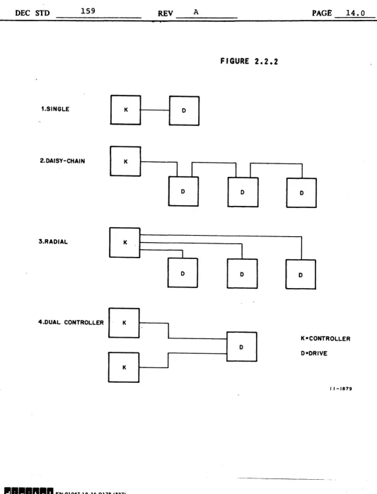
The four configurations shown In figure 2.2.1 are all expected to occur.
DEC STD 159
2.2.1.1 SINGLE
2.2.1.2 DAISY-CHAIN
2.2.1.3 RADIAL
2.2.1.4 DUAL CONTROLLER
REV A PAGE 13.0
One controller and one drive; this could be a special case of daisy-chain or radial, below.
One bus Is threaded among the several drives.
A separate bus connects each drive
with the controller.
1.SINGLE K
2.DAISY-CHAIN K
3.RADIAL K
4.DUAL CONTROLLER K
K
mamBD!a
EN-OI047-1A-16-R17S-(327) ORA U8Ao
J
I
0
I
0
l
I
FIGURE 2.2.2
I
I
1
0 0
1
0 0
K-CONTROLLER 0
D-ORIVE
[image:14.613.38.571.55.753.2]DEC STD 159 REV A PAGE 15.0
2.3 PHYSICAL CONSTRAINTS
2.3.1 The following goals are expected to be achieved by desllns conforming to this specification.
2.3.1.1 Data rates of up to 36 MHz (bits).
2.3.1.2 Up to eight drives addressable per controller.
2.3.1.3 Cable (Massbus) lengths of up to 160 feet (allowing 10 feet per drive In the daisy-chain configuration).
2.4 GENERAL ABSTRACT
2.4.0 The following are the main features of the Massbus.
2.4.1 The Massbus Is composed of two sections, containing a total of 55 signals. The data bus section, for hlsh-speed data transmission, consists of a 19 bit parallel data path and six control lines. The control bus section, for control and status Infonnatlon transfer, contains a 17 bit path and 14 control lines.
2.4.2 Each drive contains up to thirty-two addressable resisters (some drives may Implement only a subset of these). Some of these registers, when written Into, control the normal and maintenance operations of the drive. All registers may be
read from, to obtain status Information.
2.4.3 A sector format (for disk and drum) ·Is specified containing header and data records. The length of the header record Is fixed and specified (for those drives which Implement It). The length of the data record Is not specified, and ·conslderable effort has been made to avoid Implicit
restrictions on Its length.
~lmBDII!ID EN-OI047-1A-16-R17S-(327)
3.
3.1 3.1.1
3.2 3.2.1 3.2.1.1
3.2.2 3.2.2.1
3.2.3 3.2.3.1 3.2.3.2
5.2.4 5.2.4.1 5.2.4.2
5.2.5 5.2.5.1
5.2.6 5.2.6.1
5.2.7
THE CONTROL BUS INTRODUCTION
The ·purpose of the control bus Is to transmit control commands and Information from controller to drive; to transmit status
Information from drive to controller; to notify the controller when an unusual (attention) condition exists In one or more drives; and to provide a master reset (all drives) signal from the controller.
CONTROL BUS SIGNALS
Control (C (0:15»; Bidirectional
These 16 bidirectional lines carry the control and status
I nformat Ion.
Control Parity (CPA); Bidirectional
This bidirectional line carries a parity bit associated with the control lines (odd parity).
Drive Select (OS (0:2»; Controller To Drive
These three lines select the drive to be accessed.
When the Register Select lines RS(0:4) • 04(base 8), the Drive Select lines are Ignored and all drives respond. This Is for transmission of the Attention Summary psuedo register bits. Register Select (RS <0:4»; Controller To Drive
These five lines select a register In the selected drive.
When the selected register RS (0:4) • 04(base 8), each drive gates out only one bit: Its Attention Active (ATA) bit Is driven onto one of the control lines In the bit position corresponding to the drive unit number.
Controller To Drive (CTOD); Controller To Drive
This line selects the direction of transfer. It Is asserted when the transfer Is from controller to drive.
Demand (OEM); Controller To Drive
This line Is asserted by the controller to Initiate a transfer "handshake".
Transfer (TRA); Drive To Controller
DEC STD
3.2.7.1
3.2.7.2
3.2.1 3.2.8.1
3.2.9 3.2.9.1
3.2.9.2
3.2.9.3
3~2.10
159 REV A PAGE 17.0
This line Is asserted by the selected drive to complete a transfer "handshakeu •
When the selected re.lster RS (0:4) • 04(base 8), this line Is asserted by each drlve# but the controller Ignores the assertion. Instead, the controller completes the transfer after It "times out". This Is necessary because each bit on the control lines Is coming from a different drive.
Attention (ATTN); Drive To Controller
This line Is asserted by a drive when It has an "Attention Active" condition. One or more drives may assert It at the same time.
Initialize (INIT); Controller To Drive
When this line Is asserted by the controller, all drives perform a reset function.
The purpose of the Initialize line Is to give an easy way to clear all drives at once; to allow Initialization of the drives at system startup time; and to allow clearing of transIent faults.
INIT should never be asserted while RUN Is asserted. Fall (FAIL); Controller to Drive
3.2.10.1 This line Is asserted by the controller when power falls In the controller. It Is negated when 'power In the controller Is ok. The drive should Ignore assertions of DEM and INIT while FAIL Is asserted. See Section 11.5.1 for further detalls~
3.3 SEQUENCE AND TIMING OF CONTROL BUS TRANSFERS 3.3.1 Introduction
3.3.1.1 The flowcharts and timing diagrams below describe the normal operation of the control.bus. In this section, "read" means a transfer from a drive register to the controller, and "write" means a transfer the other way.
3.3.1.2 Not all resisters are Implemented In all drives. When t·he register selected by the RS lines Is unimplemented, the drive will still respond with the normal sequence shown In 3.3.4 and 3.3.8 below. After the sequence Is complete# the drive will set the Illegal Register (ILR) error bit (see section 7). Zeros are transmitted on the C lines on a control bus read; on a write, the bIts on the C lines are checked for parity, but are otherwise Ignored.
3.3.1.3 Some registers are desllnated as read only. Performing a control bus write to one of these rellsters will not cause an error; the bits on the C lines are checked for parity, but are otherwise Ignored.
3.3.1.4 While a drive Is busy (DRY bit Is reset), most registers cannot be modified by writing. The exceptions to this are the Attention Summary register, and possibly the Maintenance register (depending on the drive designer's specification). Performln, a control bus write to an unmodlflable register while the drive Is busy will cause the. Register Modification Refused (RMR) error, after the normal sequence has been completed. The bits on the C lines are checked for parity, but are otherwise Ignored.
3.3.1.5 The maximum cable delay time between controller and drive Is
375 nanoseconds, assumlnl a S5 nanosecond driver and receiver delay and a 2 nanosecond per foot propagation delay over a 160 foot length. The minimum cable delay Is O. In the flowcharts below, wherever a flowline crosses between controller and drive, Imagine a "butterfly" exists specifying max 375, min 0, over which the designer has no control.
3.3.1.6 The normal "handshake" sequences for control bus reads and writes are described In 3.3.2 and 3.3.6. Several unusual conditions can occur which will modify this sequence. One Is addressing the Attention Summary register (see 3.3.5 and 3.3.9). Another Is when the selected drive does not exist (see 3.8.1); this Is the "Nonexistent Drive" error condition.
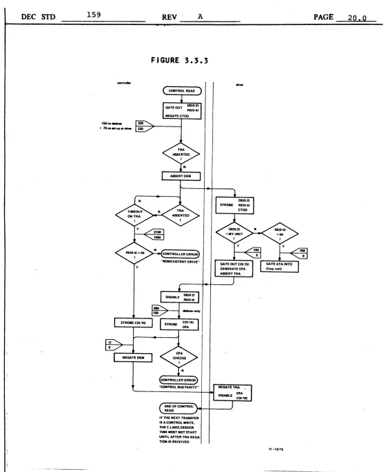
3.3.2 Control Bus Read Sequence
5.3.2.1 Refer to 3.3.4 for a timing diagram of this sequence. A flowchart of the sequence Is shown In 3.3.3. This flowchart
Includes timing restrictions In a notation described In 1.4.
5.3.2.2 The normal read sequence Is as follows.
1. The controller asserts the appropriate OS and RS lines and negates the CTOD line.
2. After waiting the deskew and set up time (min 225, max 325) and waiting, If necessary, for the TRA line to be negated, the controller asserts OEM.
3. After a cable delay, the selected drive receives the OEM assertion. 75 nanoseconds of set up time has been allowed so that the drive may use the DEM assertion edge as a strobe on the output of Its OS lines comparator and Its RS lines decoder. The controller should hold the DS and RS lines constant until the assertion of TRA Is received.
, mamBDI!ID
EN-OI047-1A-16-R175-(327)DEC STD 159 REV A PAGE 19.0
4. Not more than 500 nanoseconds later (700 for dual controller drives), the drive has gated the contents of the selected register onto the C lines and has generated CPA. It asserts TRA (each C line and CPA must be held steady until step 7).
S. After a cable delay, the controller receives the TRA assertion. The controller may disable or change the OS, RS, and CTOO lines now (If the next control bus cycle Is a read, the deskew of OS, RS, and CTOD for the next cycle may begin at this time).
6. After waiting for deskew time (min 150, max 250), the controller strobes or gates In the C lines and CPA. Parity checking may begin at this time.
7.
The controller may negate DEM at this time, or It may delay the negation of OEM In order to gate the Clines through without bufferlnl.
After a negation. TRA.
cable delay, the selected drive receives the OEM It disables the C lines and CPA and negates
-.troller
mamaama
EN-OI047-1A-16-R175-(327)~ ORA U8A
FIGURE 3.3.3
IF THE NEXT TRANSFER IS A CONTROL WRITE, THE C LINES DESKEW TIME MOST NOT START UNTIL AFTER TRA NEGA· TlON IS RECEIVED.
[image:20.612.28.581.46.725.2]DEC STD 159 REV A PAGE 21.0
FIGURE 3.3.4
CTOD (C)(T)
@R
NEXT CYCLE---'os (0:2HC)(T)}W0m ... _ _ _ SELECT LINES VALID - -___ a ~NEXT CYCLE---'
RS (0:4)(C)(T) ~ ~~
I-
DESKEW FOR NEXT _CYCLEC (~~:~ (C)(R)
fSTROBE(C)
---..;1'- - ..,
CONTROlLER MAY DELAY· NEGAnON OFOEM (C)(T) a....-DEM IN ORDER TO GATE CLINES
_ _ _ _ _ ... I THROUGH WITHOUT LATCHING
TRA (C)(R)
oS(O:2.., ~
RS(0:4r DHR)
OEM (D)(R)
TRA (o)(T)
•
L
_ - - - CYCLE TIME- {2575ns.x+, MAX _ _ _ _ _ _ _ _ .
375nl.z MIN •
MAX: 1225+ xl MI N: 225 T
375 o CABLE DELAY
I 700 I
T z ,.
375 1150.YI
o I1501 375 .0 .
*
'**t
t
t
1 2 3
(C)· AT THE CONTROLLER (T) - TRANSMITTING (D)-AT THE DRIVE (R)-RECEIVING
CABLE DESKEW DELAY
t
1
f
4 5 6 CABLE DELAY
*
DESKEW AND SET-UP**
DRIVE RESPONSE TIME1 375
l 0 DESKEW CABLE FOR NEXT DELAY CYCLE
t
t
7 8
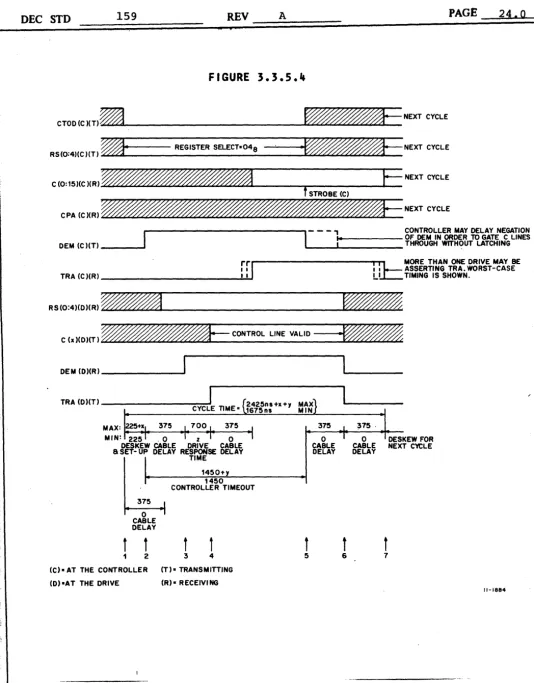
[image:21.617.39.597.61.732.2]3.3.5
3.3.5.1
3.3.5.2
S.3.5.3
Reading The Attention Summary Register
The Attention Summary register Is not a normal register. It Is composed of one bit In each of UP to eight drives. When
this register (04) Is read by the controller, each drive gates Its ATA bit out onto one of the C lines (drIve 00 onto COO, etc.).
Because all drives are responding at once, the normal handshake sequence Is not valid. Instead of using the TRA assertion as a "ready to read" signal, the controller walts for the maximum delay time and then unconditionally strobes the C lines. The controller nelates DEM after It has strobed the C lInes. No drive may disable Its C line output until It has negated TRA (typically after receiving the negation of DEM). When ·the TRA line becomes negated at the controller (after each drive has negated TRA)# the controller knows that the cycle Is complete.
Since no single drive Is generating all of the C bits, It Is Impossible for any drive to generate a valid parity bit. Therefore, the controller must Ignore the CPA line and must not check parity when reading the Attention Summary register. The sequence for reading the Attention Summary register Is as follows Crefer to 3.3.5.4 for a timing diagram of this sequence).
1. The controller asserts code 04(base 8) on the RS lines and negates the CTOD line (the state of the OS lines does not
matter). . .
2. After waiting the deskew and set up time (min 225, max 325 nanoseconds) and waiting, If necessary, for the TRA line to be negated, the controller asserts DEM.
3. After cable delay, each drive receives the DEN assertion. 75 nanoseconds of set up time has been allowed so that the drive may use the DEM assertion edge as a strobe on the output of Its RS lines decoder. The controller should hold the RS lines constant until the assertion of TRA Is
received.
4. Not more than 250 nanoseconds after receiving the DEM assertion, each drive lates out Its ATA bit onto a Cline, and asserts TRA (the C line must be held steady until step
6).
DEC STD 159 REV A PAGE 23.0
for, the controller does not use the TRA assertion to start deskew. Jnstead, It walts at least 1450 nanoseconds from the assertion of DEM (step 2). At this time, the controller strobes the C lInes and negates DEM (but does .not check parity). The controller may disable or change the DS, RS, and ClOD lines now (If the next cycle Is a read, the deskew of DS, RS, and CTOD for the next cycle may begin at this time).
6. After cable delay, each drive receives the OEM negation. It disables the C line It was driving and negates TRA. 7. After cable delay, the controller finally receives the
negation of TRA after all drives have negated It. This completes the Attention Summary register read cycle.
FIGURE 3.3.5.4
CTOD(C)(T)~
:00J ... - - - -REGISTER SELECT-04 8 RS(0:4)(C)(T) ~
C (0: 15)(C )(R)
~NEXTCYCLE
---'--".~NEXT CYCLE
f STR08E (C)
ENEXT CYCLE
~---__ - - - , CONTROLLER MAY DELAY NEGATION
I
,
... ---
OF DEM IN ORDER 10 GATE CLINES OEM (C)(T) _ _ _ --' L... _ _ -I~~ _ _ _ _ _ THROUGH WITHOUT LATCHINGIr. Irl
r"'1---"I""IU:::r""I
I I MORE THAN ONE DRIVE MAY BE ASSERTING TRA. WORST-CASE TRA(C)(R) _ _ _ _ _ _ _ _ _ _ _ _ _ ..:..:..J LI TIMING IS SHOWN.RS(0:4)(D)(R)
~
~~CONTROL LINE VALID =:W~
C (x)(D)(T)""=""~""~""~"""""W""~~_~ _ _ _ _ _ _ _ _ _ ==:Y0 __ ~"'W/#~_~///////;~~. OEM (D)(R) _ _ _ _ _ _ ---'
TRA (D)(T) _ _ _ _ _ _ _ _ _
--'I
(2425 + MAX') CYCLE TIME-H675~: x+y MIN] MAX: 225+xl 375 I 700 1 375 IMIN: 225l . 0 "I z 1 0 1
DESKEW CABLE DRIVE CABLE 8 S l ; : E T -U. P DELAY RE~r~SE DELAY
14501-Y 1450 CONTROLLER TIMEOUT 375
o
CABLE DELAY
f
t
t
t
2 3 4
(C) - AT THE CONTROLLER (T) - TRANSMITTING (D)-AT THE DRIVE (R)· RECEIVING
t
5
375 .1
o I
CABLE DELAY
t
6
~75 .
o
CABLE DELAY
f
7
DESKEW FOR NEXT C'ttLE
[image:24.624.33.567.59.742.2]DEC STD
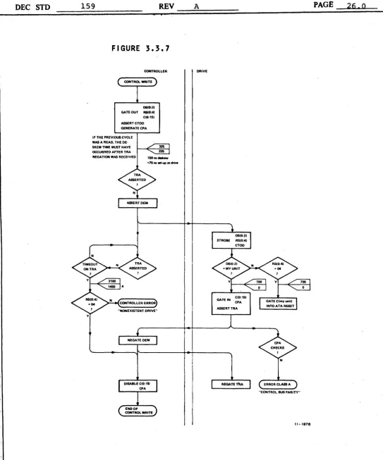
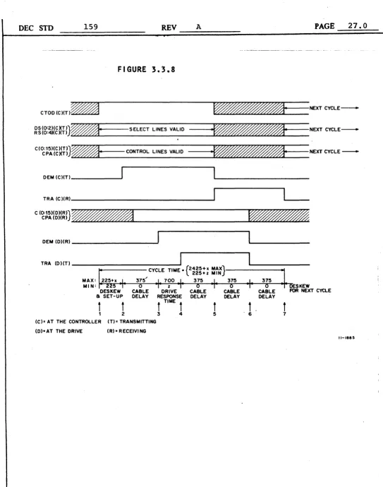
3.3.6
3.3.6.1
3.3.6.2
159 REV A PAGE 25.0
Control Bus Write Sequence
Refer to 3.3.8 for a timing diagram of this sequence. A flowchart of the sequence Is shown In 3.3.7. This floWchart
Includes timing restrictions In a notation described In 1.4.
The normal write sequence Is as follows.
1. The controller asserts the appropriate OS and RS lines, asserts the CTOD line, and gates out a word on the Clines
(the C lines and CPA must be held steady until step 5).
2. After waiting the deskew and set up time (min 225, max 325 nanoseconds> and waiting, If necessary, for the TRA line to be negated, the controller asserts DEM.
3. After a cable delay, the selected drive receives the DEM assertion. 75 nanoseconds set up time has been allowed so
that the drive may use the DEM assertion edge as a strobe on the output of Its DS lines comparator and Its RS lines decoder. The controller should hold the OS and RS lines constant until the assertion of TRA Is received.
4. Not more than 250 nanoseconds later, the drive has strobed or gated In the C lines and CPA. It asserts TRA. Parity· checking may begIn at thIs time.
5. After a cable delay, the controller receIves the TRA assertion. It negates OEM. The controller may disable or change the OS, RS, CTOD, and C .11 nes now, and beg I n the deskew for the next cycle. .
6. After a cable delay, the selected drive receives the OEM negation. It negates TRA.
7. After a
negation. cable delay, thIs completes the control bus write cycle. the controller receives the TRA
Y
FIGURE 3.3.7
CONTROLLER
0510:21 GATE OUT "!I10:41 CIO:151 ASSERTCTOD GENERATE CPA
IF THE PREVIOUS CYCLE WAS A READ, THE DE· SKEW TIME MUST HAVE OCCURRED AFTER TRA
NEGATION WAS RECEIVED 150n ... _
+75 ns set ... p at drive
----_._---:---....---mamBDma
EN-OI047-1A-16-R175-(327) ORA USADRIVE
N
"CONTROL BUS PARITY"
[image:26.617.36.580.61.715.2]DEC STD 159 REV
FIGURE 3.3.8
CTOD
(C)(T)~
C(O~~~~g~iD~~'---CONTROL LINES VALID
OEM (C)(T} _ _ _ _ _ _ ....I
A PAGE 27.0
~"'---NEXT
CYCLE---~'~"'---NEXT
CYCLE---~'~"'---NEXT
CYCLE-TRA (C)(R) _ _ _ _ _ _ _ _ _ _ _ _ _ _ _ _ _ _ ...
C (O:15)(D)(R»)~
CPA (D)(R)
OEM (D)(R) _ _ _ _ _ _ _ _ _ _ --'
TRA (DHT) _ _ _ _ _ _ _ _ _ _ _ _ _ _
1
, f 2(Cl: AT THE CONTROLLER ( n : TRANSMITTING (D)" AT THE DRIVE (R) ,. R ECEIVI NG
z
DRIVE RESPONSE
f
TIME1
3 4
CABLE DELAY
f
5
CABLE DELAY
1
6
CABLE DELAY
DESKEW FOR NEXT CYCLE
f
7
[image:27.613.36.579.47.737.2]3.3.9
3.3.9.1
3.3.9.2
3.3.9.3
Writing The Attention Summary Register
Writing Into the Attention Summary register has the special purpose of resetting selected ATA bits In the drives. This reg·lster (04) Is composed of one bit In each drive; when It Is written Into, each drive gates In one of the C lines (COO Into drive 00, etc.). If the line Is asserted, that drive will reset Its ATA bit (If the line Is negated, the drive does not change the state of ATA).
Because all drives are responding at once, the normal handshake sequence Is not valid. Instead of using the TRA assertion as a "data received" signal, the controller holds
the C lines valid for the maximum delay tIme (at least 1450 nanoseconds) and assumes that they are received by that time. Since all C bits are coming from the controller In this case, the controller generates a valid parity bit on the CPA line. The drives will check the parity as r In a normal write sequence.
The sequence for writing the AttentIon Summary register Is as
follows (refer to 3.3.9.4 for a timing diagram of this
sequence) •
1. The controller asserts code 04(base 8) on the RS lines, asserts the CTOO line, and gates out the C lines and CPA (the state of the 'OS lines does not matter). The Clines and CPA must be held steady until step 5.
2. After waiting the deskew and set up time (min 225, max 325 nanoseconds) and waiting, If necessary, for the TRA line to be negated, the controller asserts OEM.
3. After cable delay, each drive receives the OEM assertion.
75 nanoseconds of set up time has been allowed so that the drive may use the OEM assertion edge as a strobe on the output of Its RS lines decoder The controller should hold the RS lines constant until It has strobed the C lines and negated OEM.
4. Not more than 250 nanoseconds· after receiving the OEM assertion, each drive gates In the C lines and CPA, and asserts TRA. The assertion of the appropriate one of the C lines Is used to reset ATA In each drive. Parity checkln, may be done at,thls tIme.
5. After cable delay, the controller receives the TRA assertion. from the nearest (or fastest) drive. However, since other drives must also have time to respond, the controller doe. not use the TRA assertion to terminate the
-'amaD~D EN-OI047·1A·16·R175·(327)
DEC STD 159 REV A PAGE 29.0
cycle. Instead, It walts at least 1450 nanoseconds from the assertlon of OEM (step 2). At this time the controller nelates OEM.
The controller may disable or change the DS, RS, CTOD, and C lines now, and begin the deskew for the next cycle.
6. After a cable delay, each drive receives the DEM nelatlon, and negates TRA.
7. After all drives have negated TRA and after cable delay, the controller finally receives the TRA negation. This completes the Attention Summary register write cycle.
FIGURE 3.3.9.4
CTOD(C)(T)
~
~NEXT CYCLERS(0:4)(C)(T) ~~.---REGISTER SELECT 04 8 - - -... ~ NEXT CYCLE
C(0:15)(C)(T>\~ ~
CPA (C)(T1~~·---CONTROL LINES VALID ---".~NEXT CYCLE
OEM (C )(T) _ _ _ _ ..,jl
rTI
TRA (C )(R) _ _ _ _ _ _ _ _ _ _ _ ... '...1.'....1.
RS(0:4)(D)(R)
~
C(X)(D)(R)~
f STROBE (D) OEM (D)(R) _ _ _ _ _ _ ---11
MORE THAN ONE i I
V
DRIVE MAY BE ASSERTING I I TRA WORST CASE TIMING L .J. IS SHOWN~
I
TRA (D)(T) _ _ _ _ _
----JI
(:
~)
I
CYCLE TIME = 2425n5+x+y MAX I 1675n5 MIN
MAX MIN
225
1-11 375 J 700 J 3751
2,i5 CAgLE I -M~ I CAgLE -I DELAY DELAY
375 J
o CABLEl DELAY
r r
2
1450+v 1450 CONTROLLER TIMEOUT
r r
3 4
375 J 375
1
o 1 .0IDESKEW CABLE' CABLE FOR DELAY DELAY NEXT
CYCLE
r
r
r
5 6 7
(C) = AT THE CONTROLLER (T) = TRANSMITTING
*
DESKEW a SET-UP (0)= AT THE DRIVE (R) = RECEIVINGmomODJ!lD
EN-OI047-1A-16-R175-(327)irI
ORA U8A**
DRIVE RESPONSE TIME11-1880
[image:30.620.43.555.89.756.2]---DEC STD
3.4 3.4.1 3.4.1.1
3.4.2 5.4.2.1
5.4.2.2
5.4.3 5.4.3.1
5.5 5.5.1
159 REV A PAGE 31 0
COMMAND INITIATION General
To Initiate a command In a drive, the controller (or the CPU, via the controller) writes a word Into the Control register
(00) of the drive. This word will contain a command code In bIts 1 through 5 and a GO bit (always set, when starting a command) In posItion
o.
The drive begins executing the command (If It Is a valid one) as soon as the OEM line Is negated on the control bus write which loaded the controlregister.
Command codes fall Into two classes: non data transfer commands (such as Drive Clear, and Seek) and data transfer commands (such as Read Data). Bits 0 through 5 (Including the GO bit) are 01 through 47(base 8) for non data transfer command codes; 51(base 8) through 77(base 8) are for data transfer codes (see section 6 for a description of commands and their codes).
Non Data Transfer Commands
Non data transfer commands have effect only on the state of the drive. The controller merely writes the command word Into the drIve as It would for any register. At the completion of the command execution, the drive typIcally raises an attention conditIon In order to signal Its completion (see section 10
for a description of the attention condition).
If the non data transfer command code written Into the drIve Is not recognized by the drive as a valid command, the drive will normally signal an error by raising an attention
conditIon.
Data Transfer Commands
When any data transfer command Is written Into a drive, the controller expects data transfer on the data bus to begin soon thereafter. Normally, the controller will set a "controller busy" status bit related to the data bus as soon as the data transfer command code Is written Into a drive. Data transfer then follows, as descrIbed In section 4. See also section 10
for notes on programming related to data transfer. THE ATTENTION LINE (ATTN)
3.5.2
3.5.3
3.5.4
3.6
3.6.1
3.6.2
3.6.3
3.6.4
3.7
3.7.1
3.7.2
3.7.3
Inspect the Attention Summary regIster and proceed from there.
Whenever the ATA bit In a drIve Is set, that drive Is also assertIng the AttentIon line. Up to eight drives may be asserting the Attention lln~ at one time.
Drives do not set the ATA bit (and therefore do not assert the Attention line) while they are executing commands of any sort (the drive ready (DRY) status bit Is set whenever ATA gets set). No Internally generated changes of status should normally occur In a drive after It has set Its ATA bit. .
See section 8.1 for treatment of the attention condition when operating with dual controller drives.
THE INITIALIZE LINE (INIT)
The Initialize line Is used to perform a "system reset" of all drives attached to a controller. This line may be asserted by the controller at any time; however, the controller may not assert INIT and RUN simultaneously (see sec. 4.2.5.3).
When the INIT line Is asserted by the controller, It will have a minimum pulse duration of 400 nanoseconds.
When a drIve receIves the assertIon of INIT, It ImmedIately aborts the execution of any ongoing command and then performs all functions described for the drive clear command (see 6.2.1.7).
In dual controller drives, a drive whIch Is switched to controller B does not respond to the assertion of INIT on controller A, and vice versa.
CONTROL BUS PARITY CHECKING
Both the controller and the drive normally generate and check parity on control bus transfers. The CPA line Is asserted or not to make an odd modulo 2 sum of the sixteen C lines and the CPA line.
When the controller reads the Attention Summary register (04), correct parity cannot be generated because not all C bits are being generated In one drive. Therefore, the controller must
Ignore the result of parity checking In this case.
All drives and controllers will have a means of dlsabllnc parity checking while otherwise operatlnc normally. The purpose Is to permit smaller, limited feature controllers or drives which do not contain parity circuitry to operate with standard drives or controllers.
DEC STD
3.7.4
3.8
3.8.1
3.8.2
I .
3.8.3
,3.8.4
159 REV A PAGE 33.0
Note: Not all current drives contain this feature.
When a control bus parity error Is detected during a write Into a drive register, the register should be loaded, and then PAR (or the appropriate error Indicator) ERR, and ATA are set. In the case of a write Into the Control register (00), the register should be loaded, but detection of a control bus parity error should Inhibit the setting of the GO bit, and no command execution should occur.
OTHER CONTROL BUS TIMING CONSTRAINTS
If the controller selects a drive (05(0:2» which Is not present, there will be no response to the OEM assertion. The controller should walt a minimum of 1450 nanoseconds after asserting OEM before declaring the error. It Is recommended that this time not exceed 1800 nanoseconds.
These times are the same as shown above for the timeout In reading and writIng the Attention Summary register. The same timer circuit may be used for both. The error will not occur when reading or writing the attention summary register.
The OEM line Is always negated durIng the first deskew portion of the control bus timing cycle. Therefore, It Is always negated for at least 225 nanoseconds before being asserted. Because all of the timing of the control bus Is based on a maximum electrical length of 160 feet, It Is not possible to extend the Massbus beyond this leng~h, such as by using bus
repeaters.
Controllers and drives must Insure that, when they are generating them, the signals on each of the C lines and on CPA are fixed and stable (either asserted or negated) from the time they are gated out unt 11 the OEM 11 ne Is neg·ated. Th I s may require that certain status lines be buffered or latched when their states are being gated onto the Clines.
~BmDDI!'D EN-OI047-1A-16·R17S-(327)
4.
4.1
4.1.1
4.2
4.2.1
4.2.1.1
4.2.2
4.2 .• 2.1
4.2.3 4.2.3.1
4.2.4
4.2 .• 4.1
4.2.5
4.2 .• 5.1
THE DATA BUS INTRODUCTION
The. purpose of the data bus Is to transmit blocks of data at high speed between the controller .nd drive. and to control the Initiation and termination of block trans.lsslons. Data transmission Is "synchronous".
DATA BUS SIGNALS
Data (0(0:17»; Bidirectional
These lInes carry 18 bits of data between controller and drive.
Data Parity (OPA); Bidirectional
This line carrIes a parity bit associated with the Data lines (odd parity).
Sync Clock (SClK); Drive To Controller
This line carries a clock sIgnal, generated by the drive, whIch controls the gating and strobing of data on the Data
lines.
Write Clock (WCLK); Controller To Drive
This line returns the Sync Clock (SClK) signal to the drive during transmission of data from controller to drive. It tells the drive when to strobe the data lines during a write. Run (RUN); Controller To Drive.
This line controls the start-up and continuation of data transfer commands.
4.2.5.2 The RUN line Is first asserted by the controller to start the execution of a data transfer command which has been placed In the Control register of a drive. Thereafter, the drive Inspects the RUN line at the trailing edge (negation) of each EBl pulse; If the RUN line Is stIll asserted, the operation normally continues.
_~2.5.3 RUN should not be asserted while INIT Is asserted.
4u2.6
4.2.6.1
End Of Block (EBl); DrIve To Controller
This line Is pulsed by the drive at the end of each block (sector or record) of data transmitted. At the~rallln, edge
DEC STD
4.2.6.2
4.2.6.3
4.2.6.4
4.2.7
4.2.7.1
4.2.7.2
4.2.7.3
4.2.7.4
4.2 .• 8
4.2.8.1
4.3
4.3.1
159 REV A PAGE 35.0
(negation) of the pulse, the drive Inspects the RUN line. If RUN Is asserted the drive continues to read or write. If RUN Is negated, the drive terminates the operation and disconnects from the data bus.
The EBl line Is always pulsed at least once by the drive which Is commanded to read or write. This Is necessary, even In case of error, so that the controller can tell when the drive has disconnected from the data bus.
The duration of an EBl pulse Is at least 1.5 microseconds. This Is long enough to allow the controller to respond to the leading edge by negating the RUN line, and have the negation safely recognized when the trailing edge occurs.
After a drive has disconnected from the data bus (at the negation of an EBl pulse), no more state changes shall occur due to the data transfer operation just terminated.
Exception (EXC); Bidirectional
This line Is asserted by a drive performing a data transfer to Indicate that an error condition has been detected.
Once asserted by a drive, the EXC line remains asserted until the trailing edge of the last EBl pulse.
The time from the assertion of EXC to the trailing edge of the next EBl pulse must not be less than 1.5 microseconds. This Is to allow the controller time to respond to the EXC assertton safely before the drive ne~t Inspects the RUN line. The EXC line may be asserted by the controller In order to abort a data transfer command, but the controller may not assert EXC and RUN simultaneously.
Occupied (OCC); Drive To Controller
OCC Is asserted by the drive as soon as a valid data transfer command Is recognized and accepted. It Is negated at the trailing edge of the last EBl pulse.
NOTE:
OCC assertion Is not conditional on receiving RUN assertion.
SEQUENCE AND TIMING OF DATA BUS TRANSFERS Introduction
4.3.1.1
4.3.1.2
4.3.1.3
4.3.1.4
4.3.1.5
4.3.2
4.3.2.1
The data bus Is used for transmission of data from and to the drive recording medIum. Timing of transfers Is controlled by a clock which Is generated by the drive.
Tra~sfers are oriented towards blocks of data which are transmItted as a group (e.g., sectors on a disk, records on mag tape). The drive will normally send and receive data only as whole blocks. If the number of data words desired by the CPU Is not an Integral times the number of words per block, It Is up to the controller to stop the transfer to memory on reads or to provide filler·words on writes.
The data bus Is shared among all drives. Only one drive may be attached to It at a time. The controller should prevent a data transfer command from being loaded Into a drive while OCC
Is asserted.
A drive attaches Itself to the data bus and asserts OCC when a data transfer conmand Is loaded Into Its Control regIster. After transferring one or more blocks of data (unless a class B error occurs), the drive disconnects from the data bus and negates OCC. Disconnect always occurs at the traIling edge
(negation) of an EBl pulse.
For detailed description of error conditions and theIr effects on data bus signals, see· section 7.
Data Bus Read Sequence
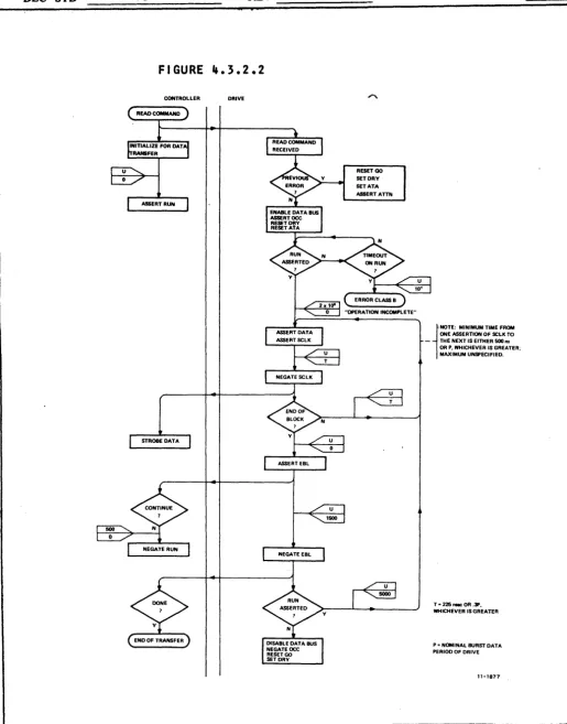
This section describes a typical data bus read sequence with no errors. 4.3.2.3 Is a timing diagram of a read of a single sector with four words. 4.3.2.2 Is a flowchart, with timing restrictions, of the read sequence. The following sequence occurs on a data bus read Crefer to 4.3.2.3).
1. A read command Is loaded Into the Control register of the drive. If the command Is valid, the drive enables Its data bus receivers and drivers and asserts OCC.
2. Not more than 100 microseconds after step 1, the controller asserts RUN.
3. After a cable delay, the drive receives the RUN assertIon. DIsk drives now begin searchIng for the desIred sector. Tape drives begin tape motion.
4. When the drIve has read the first data word and gated It
onto the D lines, It generates DPA and asserts SClK.
5. After a cable delay, the controller receives the SClK assertion.
DEC STD
6.
159 REV
The drive nesates SCLK asserting It, where percent of the nominal whichever Is greater. valid for no less than SCLK Is negated.
A PAGE 36.0
no less than T nanoseconds after T Is either 225 nanoseconds or 30 burst data period of the drive, The Data lines should be maintained one half of the SCLK Interval after
7. After a cable delay, the controller receives the SCLK negation. The controller strobes the D lines and OPA, and checks the parity.
8. If there Is more data to be read In this block, then not less than T nanoseconds after step 6, the drive gates out the next data word onto the 0 lines, generates OPA, and 'asserts SClK. Steps 5, 6, and 7 then follow.
9. After the negation of SCLK (step 6) on the last word of data In the block, the drive asserts ESl.
10. After a cable delay, the controller receives the ESl
assertion. At this time, the controller must' decide whether or not to have the drive read the next block of data without disconnecting from the data bus (the controller may already have negated the RUN line).
11. If the controller decides not to read the next block, It negates the RUN line not later than 500 nanoseconds after step 10.
12. After a cable delay, the drive receives the RUN negation (the RUN line may already have been negated).
13. Not less than 1500 nanoseconds after step 9, the drive negates EBL. At this time the drive strobes the RUN
line. If RUN has been negated, the drive disconnects from the data bus (the DRY bit should be set and OCC negated at this time).
14. After a cable delay, the controller receives the EBl
negation (the controller may now generate an end-of-transfer Interrupt, and start another data
transfer).
mDmDD~D EN-OI047-1A-16-R175-(327)
FIGURE 4.3.2.2
CONTROLLER DRIVE
RESET GO SET DRY SETATA ASSERT ATTN
l
'
NOTE: MINIMUM TIME FROM ONE ASSERTION OF SCLK TO - THE NEXT IS EITHER 500 n.OR P, WHICHEVER IS GREATER; MAXIMUM UNSPECIFIED.
T-225..-.0R .31', WHICHEVER IS GREATER
P = NOMINAL BURST DATA PERIOD OF DRIVE
[image:38.618.36.551.77.734.2]DEC STD 159 REV
FIGURE 4.3.2.3
0(0:17>\ ~
OPA
f
CHR)=
f
A PAGE 38,Q
f f f
RUN(C)(T) _ _ ~
I I I I I
I
I I I I I _I L_ - - 7 7 , ...
-EBl (C)(R) _ _ _ _ _ _ _ _ _ _ _ _ _ _ _ ~---~---~-~~~~
SClK (C )(R) _ _ _ _ _ _ _ _ _ ---'
occ (O)(nJ
0(0:17)\
OPA fO)(T>
~
WORD 1I
WORD 2RUN (O)(R)
EBl (O)(T)
SCLK (O)(T)
WORD 3 WORD 4
~
L
MAX:~--~~---~~~~~---~~U~~----~U~----~~
MIN: 0 1500
t
t t
f ~ff
t
11
2 3 4 6 7 6
(C) - AT THE CONTROllER(T) - TRANSMITTING (0) -AT THE DRIVE (R) - RECEIVING
'D'DDI!ID
EN-OI047-1A-16-R175-(327)~
W II
ORA USAft U
tt
tf
7 6 7 6
*
100 MICROSEC. MAX**
200 MlllSEC. MAX375
o
f
l
ft
f f
t
7 10 11 12 13 14 U· UNSPECIFIED MAXIMUM
T= 225 or 30% of P whichever is greater
p,. Nominal burst data
period of drive
4.3.3 4.3.3.1
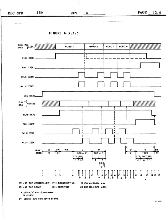
Data Bus Write Sequence
This section describes a typical data bus write sequence with no errors. 4.3.3.2 Is a flowchart of the write sequence, showing timIng restrictions. See 4.3.3.3 for a tIming diagram of a write of a single sector with four words.
The following sequence occurs on a data bus write.
1. A write conmand Is loaded Into the Control rellster of the drive. If the command Is valid, the drive enables Its data bus receivers and drivers and asserts OCC.
2. Not more than 10 milliseconds after step 1, the controller has lated the first word onto the D lInes, and has lenerated DPA. It asserts RUN.
3. After a cable delay, the drive receives the RUN assertion. Disk drives now begIn searchlna for the desired sector. Tape drives begin tape motion.
4. When the drive Is ready to accept the first word, It asserts SClK.
5. After a cable delay, the controller receives the SClK assertion. The controller asserts WClK.
6. After a cable delay, the drive receives the WClK assertion. The drive now strobes the 0 lines and DPA. (t checks parity (the drive may now.begln to write the word on the rned I urn).
7. The drive neaates SClK no less than T nanoseconds after assertIng It, whe~e T Is either 225 nanoseconds or 30 percent of the nominal burst data period of the drive, whichever Is greater.
I. After a cable delay, the controller receives the SClK nesatlon. The controller negates WClK; It then gates out
the next word on the D lines, and generates DPA.
9. After a cable delay, the drive receives the WClK nelatlon. 10. 'f more words are to be written, then not less than ·T nanoseconds after negating SClK, the drive asserts It alaln (the Interval between the fIrst and second SClK pulses shown In 4.3.3.3 Is longer than the later
Intervals, since this Is probably typical behavior for dIsk drives. The restrictions on the Intervals are not dIfferent). Steps 5, 6, 7, 8, and 9 then follow.
mamDDI!'D
EN-OI047-1A-16-R175-(327)DEC STD 159 REV A PAGE 40.0
11. After the ne,atlon of Sell (step 7) for the last word In the blockl th~ drive asserts EBl.
12. After a cable delay, the controller receives the EBl assertion. At t~ls ~Ime, the controller must d~clde
whether or not to have the drive wrIte the next block of data without disconnecting from the data bus (the controller may already have negated the RUN lIne).
13. If the controller decides not to write the next block, It negates the RUN line not later than 500 nanoseconds after step "12.
14. After a cable delay, the drive receives the RUN negation (the RUN line may already have been negated).
15. Not less than 1500 nanoseconds after step 11, the drive negates EBl. At this time the drive strobes the RUN line. If RUN has been nelated, the drive disconnects from the data bus (the DRY bit should be set and
oce
negated at this time).FIGURE 4.3.3.2
CONTROLLER ORIVE
~DmDamD EN-OI047-1A-16-R175-(327)
ORA 1I8A
U 5000
U
NOTE: MINIMUM TIME FROM ONE ASSERTION OF SCLK TO NEXT IS EITHER 500 M ORTHE - NOMINAL BURST DATA RATE
OF THE DRIVE. WHICHEVER IS GREATER; MAXIMUM UNSPECIFIED.
T = EITHER 225 M OR ~ OF THE NOMINAL BURST DATA PERIOD OF THE DRIVE. WHICHEVER IS GREATER.
[image:42.615.40.540.72.745.2]DEC STD 159 REV A PAGE 42.0
FIGURE 4.3.3.3
WORD 1 WORD 2
I
WORD:3 WORD 4I I
I I
I I I I I
I
I I I I I
11 _ _ _ _ _ 1 _ _ _ L- ___ 1 _ _ _ _ ~ _ _ _ _
I I I I
RUN (CHT) _ _ _ _ _ ~
I . I 1
I I I ,
I
1 , I 1
EBl (C)(R) ______________________________ ~I~---~I~---I~---I~--~
I 1 1 1
L
SClK (CHR) __________________________
~r__lI~
______
~~
__________________ _
WClK (C)(T) __________________________ ~r__l ~__________________ _
OCC
oHT)~
o (0:17~ (o)(R) oPA
J
RUN (oHR)
ESl (oHT)
SClK (oHT)
•
L
•
•
,
L
WCLK (oHR)
_________________
~n~_ILILJI____ __
U U
MAX:M-____ ~~~--**----~---U----~~--U--~
MIN: 5000rP o 1500
t
t
tt
1 2 3 4
(C)" AT THE CONTROllER (T)= TRANSMITTING (D) = AT THE DRIVE (R)· RECEIVING T" 225 or 30% of P, whichever
is Qreater.
P" Nominal burst data period of drive.
'amBDI!ID
EN-OI047-1A-16-R175-(327)f.:tI ~ ORA U8A
U U 375
T T o
375
o
If
7!
1 1.1 l1l1.t 1
8 9 7 8 9 . 7 8 9 7 8 9!1!
1.61
!1!
1 1.'
*
100 MICROSEC MAX.**
200 MllLiSEC. MAX.t t
t
t
t
12 13141516 [image:43.617.36.577.43.753.2]4.4.2
4.5
4.5.1
4.5.2
4.5.3
4.6
4.6.1
4.6.2
DATA BUS PARITY CHECKING
Both the controller and the drive normally generate and check parity on data bus transfers. The DPA line Is asserted or not to ,make an odd modu 1 0 2 sum of the e I gh teen D 11 ne,s and the DPA line.
All drives and controllers will have a means of dIsabling parity checking while otherwise operating normally. The purpose Is to permit smaller limited-feature controllers or drives which do not contain parIty circuitry to operate with standard drives or controllers.
Note: Not all current drives contain this feature.
ERROR SIGNALING
The EXC line Is used to signal an error condition by the drive which Is doing a data transfer while the transfer Is going on. See section 7 for a complete description of how various error conditions are handled.
The drive which Is doing a data transfer never asserts the ATTN line (of the control bus) while the data transfer Is going on. If an error occurs, the drive does assert ATTN after disconnecting from the data bus (after the DRY bIt Is set and OCC negated).
When the controller asserts EXC, It must always negate RUN; under normal condItions, the controller negates RUN whenever the EXC lIne Is asserted. See sectron 7 for descrIptions of cases where thIs may not be true, and the possIble consequences.
DATA TRANSFER COMMAND TERMINATION
Data transfer commands are normally termInated at the traIlIng edge (negation) of the EBL pulse (when the RUN line has been negated). In abnormal or error sItuatIons, the drive still
mus~ generate an EBL pulse, In order to define to the
controller when the drIve has dIsconnected from the data bus.
When a drIve negates EBL, It disconnects from the data bus If anyone of the following Is true:
1. The RUN line Is negated.
2. The EXC line has been asserted by the controller
DEC STD
4.6.3
'.6.4
4.7
4.7.1
4.7.2
4.7.3
4.7.4
4.7.5
4.7.6
159 REV A PAGE 44.0
The controller cannot distinguish 3 above from the case of a Class A error (In which the drive will continue If RUN remains asserted). Therefore, case 3 may result In a "NO SCLK" timeout after 250 milliseconds (see section 7).
In mag tape, a Frame Count register substitutes for sector detection on disks. The mag tape drive. generates an EBl pulse when the frame count becomes zero.
During data transfers, control bus writes are not permitted
Into any registers except the Attention Sunmary register and the Maintenance register.
ADDITIONAL DATA BUS TIMING RESTRICTIONS
Because the timing of the data bus Is based on a maximum electrIcal length of 160 feet, It Is not possible to extend the Massbus beyond this length, such as by using bus repeaters.
There Is a point In time for each sector (on disk) beyond which an attempt to read or write that sector will fall (on this revolution). let us call this the "Sector Decision Point". The drive should assure that the trailing edge of the EBl pulse occurs not later than 5 microseconds before the "Sector Decision Point" of the following sector. The purpose Is to allow the controller· sufficient time, after a transfer terminates on a drive, to write a new desired sector address and a new command Into that drive, and not lose a
revolution when the desired sector Is ~he next one.
When the drive asserts EXC, It must assure that (whenever EBL Is next asserted) EXC and EBL are asserted together for at least 1500 nanoseconds. This may sometimes require extending the normal duratIon of the EBL pulse.
When a severe (Class B) error occurs In a drive during a data transfer, the drive designer must take steps to assure that the SCLK, EXC, and ESl lines do not get "stuck" In the asserted state. Also, the SCLK pulse should not be allowed to "glitch" (have a very short duration) In any error case.
After the controller has asserted RUN, an error should be declared If no SCLK pulse Is received for 250 milliseconds ·or more (unless OCC Is asserted). An error should also be declared If, after RUN Is negated, no ESL pulse has occurred for 250 milliseconds or more (unless OCC Is asserted). The assertion of OCC should Inhibit both timeout errors.