System Verification of Hardware Optimization Based on
Edge Detection
Xinwei Niu, Jeffrey Fan
Department of Electrical and Computer Engineering, Florida International University, Miami, USA Email: [email protected], [email protected]
Received March 21,2013; revised April 21, 2013; accepted April 30, 2013
Copyright © 2013 Xinwei Niu, Jeffrey Fan. This is an open access article distributed under the Creative Commons Attribution Li-cense, which permits unrestricted use, distribution, and reproduction in any medium, provided the original work is properly cited.
ABSTRACT
Nowadays, digital camera based remote controllers are widely used in people’s daily lives. It is known that the edge detection process plays an essential role in remote controlled applications. In this paper, a system verification platform of hardware optimization based on the edge detection is proposed. The Field-Programmable Gate Array (FPGA) valida-tion is an important step in the Integrated Circuit (IC) design workflow. The Sobel edge detecvalida-tion algorithm is chosen and optimized through the FPGA verification platform. Hardware optimization techniques are used to create a high performance, low cost design. The Sobel edge detection operator is designed and mounted through the system Ad-vanced High-performance Bus (AHB). Different FPGA boards are used for evaluation purposes. It is proved that with the proposed hardware optimization method, the hardware design of the Sobel edge detection operator can save 6% of on-chip resources for the Sobel core calculation and 42% for the whole frame calculation.
Keywords: IC; AHB; FPGA; Hardware Optimization; Sobel Edge Detection
1. Introduction
The technology evolves rapidly in these years. Currently, people enjoy many high-tech products such as gesture based remote controller by using digital cameras to ex-tract valuable information. It is known that the edge de-tection plays an important role in the remote control process [1]. The edge detection is used to process the input data and extracts the key feature of the data for further steps. Several edge detection algorithms can be used to identify the edge of one image frame. In this pa-per, the Sobel edge detection is designed and verified by using the verification platform.
Integrated Circuit (IC) chip manufacture involves a variety of processes. The basic rules are the same even though there may be different kinds of design flows. In the IC design flow, Field-Programmable Gate Array (FPGA) verification is an important step. Benefited from the reconfigurabilities of the FPGA, designers can verify their design at the early stage of the IC design flow. Thus, design defects can be found and eliminated to save de-sign cycles and costs.
The edge detection is the most commonly used ap-proach to detect discontinuities in gray level by far. It is widely used to extract the texture of the item in one pic-ture. There are many edge detection operators based on
the gradient detection. In this research, the Sobel opera-tor for the edge detection and a verification platform is used to test the proposed hardware design.
SoCs. V. Sanduja and R. Patial designed a complete edge detection system based on the Sobel operator, and their design had an accurate result for each pixel. However, the costs of the resources are still much higher by using two separate memory parts to store the data [6].
The rest of the paper is organized as follows. In Sec-tion 2, an overview of the IC design flow and the Sobel edge detection is presented. Section 3 explains the archi-tecture of our hardware verification platform. In Section 4, the optimized hardware of the Sobel edge detection operator is evaluated, and then the verification platform is demonstrated. Finally, conclusions and future works are drawn in Section 5.
2. Background
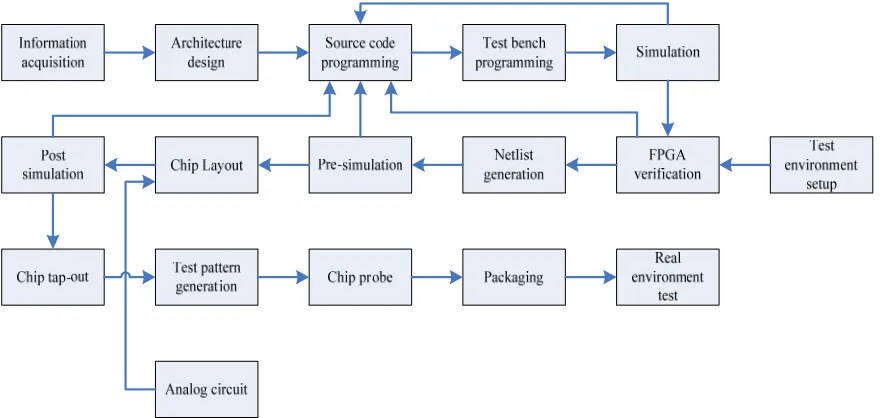
Designers put different efforts in the process of making a successful IC. As shown in Figure 1, the most important stage in the design flow is the information acquisition stage. Designers do some researches on the aimed design including specifications, algorithms and even the archi-tecture. With a clear understanding of the whole design, designers can go ahead for the next stage.
In the architectural design stage, designers must be familiar with all the related knowledge of the design. The selected algorithm is directly related to the structure, this is why we need to first verify and generate the most suitable algorithm form. The best architecture is the one with the fastest speed, the lowest power consumption and the minimum chip size.
Hardware designers use the hardware description lan-guage to write the source code. After that, designers must write the test bench for their design. Test bench provides simulation models for designs.
Then it goes to the Register Transfer Level (RTL)
simulation, which is also called behavioral simulation. It is based on the RTL function but not timing considera-tion. If a designer uses an FPGA to develop the circuit, the design code can be synthesized into the FPGA netlist. The FPGA verification with the real test environment can find most of the problems.
The design code is viewed as a good one once it passes the FPGA verification stage. Then, the code is synthe-sized into a netlist for the chip layout. After that, design-ers do simulation again, which is called pre-simulation. On the pre-simulation stage, timing issues are added to the simulation, so the simulation is closer to the per-formance of the real chip. The timing is only added to the cells and registers, but not wires. If the pre-simulation results are not as expected, the source code should be re-designed.
After the chip layout process, another netlist is gener-ated according to the real wires of the chip. With the consideration of the wire delay, the design goes to the post-simulation stage. If post-simulation results meet the design requirements, the design is ready for the chip fab-rication.
The manufactured chip is packaged and mounted in the system to check whether it is good or not. The test pattern should have higher coverage for all the possibili-ties. The higher the coverage, the better of the yield of the chip. The tester uses the probe card to check the chip on the wafer. When the chip passes the chip probe stage, the wafer can be cut down for packaging. After packag-ing, the IC chips are tested again to make sure the chips are good. The last step in the entire workflow is to test the IC mounted on the real system.
[image:2.595.79.520.510.719.2]The edge detection is the most widely used method to detect discontinuities in one image by far. An edge is a
Figure 1. IC design flow chart.
number of pixels which lie on the boundary between two regions. Edges are located in the areas with strong inten-sity contrasts. There are many edge detection operators based on the gradient detection [1]. The Sobel operator is chosen to be used for the edge detection in this paper.
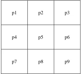
The Sobel operator is a 3 × 3 mask used to compute the gradient for the corresponding region. Figure 2 shows pixels of the aimed image region, the Sobel op-erator multiplies with the image pixels to find out the gradient at the point labelled p5.
Sobel operators are as follows:
1 0 1 2 0 2 1 0 1
G A
1 2 1
0 0 0
1 2 1
G A
x
(1)
y (2)
As shown in the Equations (1) and (2), A is the gray-scale of the original images. The Gx is the row gradient and the Gy is the column gradient. An approach used frequently is to approximate the magnitude of the Sobel gradient by absolute values:
x y
f G G
(3)
After generating the value of the Equation (3), the re-sult is compared with a threshold, which sets the final value to either black or white. The result is sent back to the image point labelled p5 for one round calculation.
3. System Architecture
In this research, the Sobel operator is used to detect the edge of a 256 × 256 grayscale image. The Sobel opera-tion is separated into two parts, one part is a Sobel core, the other part is the Sobel full scan. The Sobel core is a single calculation of the matrix, and the Sobel full scan is used to scan the full image frame. The Sobel operator design is optimized for the hardware implementation from the following aspects:
p1 p2 p3
p4 p5 p6
[image:3.595.120.235.225.322.2]p7 p8 p9
Figure 2. Image region for edge detection.
The Sobel core needs higher frequency to finish the calculation in a pipeline design. In order to make the design run efficiently, the operation defines that one pixel is loaded to the Sobel core every clock cycle. After loading the input data, the Sobel operation can generate the output data in the following cycle. The Sobel core of this design needs two clock cycles to generate the result, so Sobel core part is connected to a clock, whose frequency is two times as the clock connected to Sobel full scan. Thus, the data can flow continuously without the latency.
[image:3.595.106.239.600.720.2] [image:3.595.312.533.644.720.2] The other optimization is to put the generated data to the image pixel labelled p1 instead of p5 as shown in Figure 3. The design can have a higher efficiency by using this way. After the calculation of the single ma-trix. The Sobel mask will move to the next window, it will go through all the rows and columns in the image frame. If the generated results are sent back to p5, the Sobel mask must store the original pixel before the results are sent back. If designers want to avoid the influence of the results, they must use other storage devices to hold the results, which is a costly method. However, we store the results directly in the pixel la-belled p1. The pixel lala-belled p1 will not be used in the future, so it has no influence for the future calcu-lation even if the data is modified. Moreover, the de-signer does not need additional storage devices to keep results.
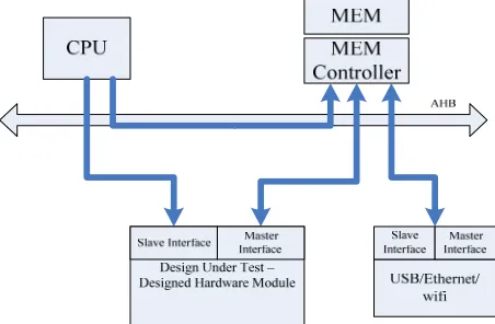
The designed hardware must be tested under the test environment, which is a system verification platform. The platform can be used to test the functionality of the design and it includes the following components:
Test module design. The Design Under Test (DUT) module is connected to the platform as a slave. Verification module design. Functional simulation of
the CPU is used to test the designed hardware. The memory controller and some external interface mod-ules are designed and verified.
Advanced Microcontroller Bus Architecture (AMBA) based protocol design. Advanced High-performance Bus (AHB) from the AMBA bus protocol is used for data transmission [7].
Functional registers design. The hardware provides configuration registers for the software designer to design the corresponding software.
Figure 4 is the system verification platform. The veri-fication platform includes the CPU, the memory control-ler, the DUT, and other interfaces. The platform uses AHB as the communication bus. Each DUT must have the slave interface and the master interface for commu-nication through the AHB bus. As the central processing unit of the system, the CPU has only the master interface to send command. As the data storage devices, memories are viewed as slaves. Thus, they only have the slave in-terfaces.
The master interface is used to send commands to the slave interfaces and receive the data or responses from the slave interfaces. In the system design, the CPU will initial the command to the DUT, which is the Sobel edge detection module in this project, through the DUT’s slave interface. The command is used to configure the func-tional registers of the designed hardware intellectual property (IP). Once the designed hardware gets the command from the CPU, it extracts the information and takes further actions. The information includes the start and the stop of the DUT, the initial address of the mem-ory or other peripherals, where the DUT can fetch data from, etc. Then, the DUT can fetch the data from mem-ory or other peripherals through its master interface to the slave interface of the memory controller. After fin-ishing processing, the DUT can send the results back to the memory or other peripherals if necessary.
4. Experimental Results
The Sobel edge detection design is divided into two parts: one is the single matrix calculation; the other is the full frame calculation. Because the single calculation needs time to process the data, the clock frequency of the in-ternal single calculation is twice as the full frame calcu-lation to make the whole data run as the pipeline. In the real case, each gate has its own timing constraint. One can only use the maximum of around six adders or sub-tractors together to generate the output data through combinational logics. Thus, the single matrix calculation
Figure 4. System verification platform.
is separated into two RTL blocks. This can not only have the least register usage but the designed circuit can also run at a relatively higher frequency.
Compared to the single Sobel operator design in [2], they designed a single Sobel operator and mapped the design on Xilinx Spartan 3 XC3S50-5PQ208 board [8]. Their design can reach up to 190 MHz frequency. In contrast, our design can only reach up to 156 MHz on the same board. However, as for the resource costs, our de-sign only occupies 10% of on-chip slices, while their design cost up to 16% of on-chip slices. In the Sys-tem-on-a-Chip (SoC), on-chip resource costs are key factors which have great impacts on the design. The less of the resource costs, the lower of the power consump-tion. If a 256 × 256 frame needs to be processed, our design can ideally consume 0.41 ms to finish, while their design can ideally consume 0.34 ms to finish. This is still an acceptable time latency in the remote control system, especially consider the saved on-chip resources.
In another design from V. Sanduja and R. Patial [6], a 20 × 40 picture was processed by the Sobel edge detec-tion design. Their design used Xilinx Virtex 4 FPGA board. The device was XC4VLX200, and the package was FF1513. Even they got the accurate result for each pixel, the design cost too much on-chip resource. Table 1 shows the device utilization comparison. It is shown that our design uses much less resources than their design. One advantage of our design is using a single RAM to store the data, after pixels are processed by the single matrix calculation. The processed result is sent back to the position labelled p1 instead of p5. This optimization method can save a large amount of storage space and the processed picture is usable for further steps in our SoC design. The other advantage is that our design does not process the rightmost two columns and lowest two rows of the picture. This can save the processing time when the data set is huge enough. Moreover, the omitted pixels have little influence to the final results.
[image:4.595.308.537.653.736.2]For the verification platform, the CPU is instantiated as a functional module, and it sends command registers to the Sobel edge detection operator. The image frame used for the experiment is a 256 × 256 grayscale picture, so there are 65,536 positions in the memory. The Sobel edge detection operator extracts the information from the command registers, so that the operator knows when to
Table 1. Device utilization comparison.
Number of Occupied Slice
Number of Slice Flip-Flops
Number of 4-Input LUTs
Design
in [6] 1987 836 3901
Proposed
Design 1144 128 1400
Figure 5 is the block design of the system. The system uses two synchronized clocks and one global reset signal. The Sobel core block is embedded in the Sobel_fullscan block. Two signals, which are do_fullscan and fullscan_ done, are reserved for future usage. If there are more than one DUTs in the system, an arbiter will be used to ac-commodate different DUTs based on the AHB protocol. The Sobel operator communicates with the off-chip memory through the ddr_controller. The Sobel core IP is integrated into the sobel_fullscan IP. Figure 6 is the simulation results from Mentor Graphic Modelsim [9]. By employing the pipeline technique, the DUT runs write and read data. The Sobel edge detection operator
also gets the information of where to fetch the data blocks. Then, the operator sends commands to the mem-ory controller to fetch the data and do calculations. The system sends the results back to the memory after finish-ing the whole image frame calculation.
The AHB bus protocol is an industry standard, so that the platform can be used for other DUTs in the future if properly configured. The transmission on the AHB bus is 32 bit. The responses of the slaves are set to okay for easy use to ensure the communication is good for this design.
Figure 6. Simulation results with system bus.
smoothly on the verification platform. The edge detec-tion part consumes nine clock cycles to fetch the desired pixels, then, the result can be generated in the tenth clock cycle. Thus, the design can not only have a shorter exe-cution time but also few resource costs.
5. Conclusions
This paper introduces a system verification platform of hardware optimization based on the edge detection algo-rithm. The Sobel edge detection operator is designed and verified on the verification platform. The IC design flow is provided to make sure the designed chip is a good one. The Sobel edge detection operator is one of the most commonly used methods in remote controller design. In this design, the Sobel operator is separated into two parts in order to process the data more efficiently and consume fewer resources. Experimental results show that the de-signed Sobel edge detection operator can save 6% of on-chip resources for the Sobel core calculation and 42% for the whole frame calculation.
The system verification platform is set up to verify the designed hardware. The verification platform is com-posed of the functional CPU module, the DUT module, the memory module and other peripherals. These mod-ules communicate with each other through the AHB bus protocol. It is proved that the designed Sobel operator works efficiently on this verification platform. The de-signed Sobel operator can be processed to the next stage to make an IC chip. The verification platform can be further used to verify other designed hardware.
REFERENCES
[1] R. C. Gonzalez and R. E. Woods, “Digital Image
Proc-essing,” 2nd Edition, Prentice Hall, Upper Saddle River, 2001.
[2] S. Halder, D. Bhattacharjee, et al., “A Fast FPGA Based Architecture for Sobel Edge Detection,” Progress in VLSI Design and Test, Lecture Notes in Computer Science, Vol. 7373, 2012, pp. 300-306.
[3] T. A. Abbasi and M. U. Abbasi, “A Novel FPGA-Based Architecture for Sobel Edge Detection Operator,” Inter-national Journal of Electronics, Vol. 94, No. 9, 2007, pp. 889-896. doi:10.1080/00207210701685253
[4] C. Pradabpet, N. Ravinu, et al., “An Efficient Filter Struc-ture for Multiplierless Sobel Edge Detection,” Innovative Technologies in Intelligent Systems and Industrial Appli-cations, 25-26 July 2009, pp. 40-44.
[5] Z. E. M. Osman, F. A. Hussin, et al., “Hardware Imple-mentation of an Optimized Processor Architecture for So-bel Image Edge Detection Operator,” 2010 International Conference on Intelligent and Advanced Systems, 15-17 June 2010, pp. 1-4.
[6] V. Sanduja and R. Patial, “Sobel Edge Detection Using Parallel Architecture Based on FPGA,” International Jour-nal of Applied Information Systems, Vol. 4, No. 4, 2012, pp. 20-24.
[7] AMBA Specifications.
http://www.arm.com/products/system-ip/amba/amba-ope n-specifications.php
[8] Xilinx Incorporated. http://www.xilinx.com
[9] MentorGraphics Modelsim. http://www.model.com
![Figure 5 is the block design of the system. The system simulation results from Mentor Graphic Modelsim [9]](https://thumb-us.123doks.com/thumbv2/123dok_us/7783876.722656/5.595.80.521.240.723/figure-block-design-simulation-results-mentor-graphic-modelsim.webp)

