STARAN S
Reference
·
Manual
-j~
~,oJ ,\~
16 January 1973
To:
Distribution
Subject:
STARAN S Reference Manual - GER-15636
The subject manual has been upgraded.
The attached pages are forwarded
for inclusion in your copy.
Please substitute the changed pages for
the existing pages.
-. ---?
~/?££/~
ij/~
(
..
(/~--~--~---~---~
L. P. Arkwright
Price $25. 00
GOODYEAR AEROSP.ACE
CORPORATION
AKRON, OHIO 44315
STARAN
S
REFERENCE
MANUAL
GER 15636
Change 1
Change 1
NOTICE
This document contains material generated by Goodyear Aerospace
Corporation and is transmitted for the purpose of aiding the transaction
of business between Goodyear Aerospace Corporation and the recipient.
It is understood that the material contained herein will not be used,
copied, or disclosed to others, without specific written consent of
Goodyear Aerospace Corporation.
DESIGN UPGRADING
The STARAN S Computer System will continue to be improved and
upgraded. Interested parties should contact Goodyear Aerospace
Corporation, Computer Division Marketing, Akron, Ohio 44315,
Telephone: (216) 794-3631 for information regarding STARAN S
design improvements.
LIST OF EFFECTIVE PAGES
Insert latest changed pages and dispose of superseded pages.
NOTE: On a changed page, the information affected by the latest
change is indicated by a vertical line in the outer margin of the
page. A zero in the change number column indicates an original
page.
The total number of pages in this manual is 157, consisting of the
following:
Page Change
No. Number
Title
A, B 1
i - ix 0
x
xi, xii 0
1-1 - 1-3 0
1-4 1
1-5, 1-6 0
1-7
1-8 - 1-10 0
1-11
1-12 - 1-14 0
1-15
1-16 - 1-30 0
LIST OF EFFECTIVE PAGES CONTINUED
Page Change
No. Number
2-1 0
2-2, 2-3 1
2-4 0
2-5
2-6 - 2-9 0
2-10 1
2-11, 2-12 0
2-13
2-14 0
2-15
2-16 0
2-17, 2-18 1
2-19, 2-20 0
2-21, 2-22 1
2-23 - 2-25 0
2-26 1
2-27 - 2-29 0
2-30 1
2-31 - 2-38 0
2-39 1
2-40 - 2-48 0
2-49 1
2-50 - 2-57 0
3-1 - 3-4 0
Ai 0
Al
A2 - A6 0
A7
A8, A9 0
A10
Bi, B1 - B11 0
Ci, C1 - C3 0
Di, D1 - D3 0
D4
D5 0
Ei, E1 - E4 0
Fi, F1 0
Gi, Gl - G2 0
X-I - X-8 0
CHAPTER
TABLE OF CONTENTS
TITLE
FOREWORD
STARAN S ARCHITECTURE
System Architecture • • • •
Associative Processor Control Memory
Associative Processor Control
Associative Array Memory •
Program Pager • • • • • •
External Function Logic
Sequential Control • • •
Input/Output Variations
Associative Processor Control Memory· •• • • • Description
General.
Page Memories • • • • •
High-Speed Data Buffer. Bulk Core Memory . . Direct Memory Access
Addressing
General.
Bulk Core Memory Page Memories • • • • High Speed Data Buffer • Branch and Link Registers Direct Memory Access ••
Associative Processor Control Memory Summary
Associative Processor Control
General
Instruction Register
Program Control
Program Counter. Start Loop Marker End Loop Marker Comparator • • Status Register
. Bus Logic
Shift Logic
Data Pointer Register Block Length Counter • • •
Common Register • •
Mask Generator ••
Field Pointers and Length Counters
Field Pointer 1 Field Pointer 2 Field Pointer 3 Field Pointer E
Field Length Counter 1 • Field Length Counter 2 •
CHAPTER
1 (cont)
TABLE OF CONTENTS
TITLE
Response Store Control • • • •
Control Line Conditioner Control Line Buffer • • • • •
Array Control
Array Select Register Array Address Select Array Mode.
Shift Control
Resolver
Associative Arrays
General Description
Addressing
Arrays Words Bit Columns Fields ••
Operations • • • •
Loads • • • • Masked Store Logical. Resolve.
Program Pager
General ••
Operation
External Function Logic •
General • • • • • • • •
Page Memory Port Switches
Interlocks • • . •
Program Pager •
Error Control • •
Associative Processor Control Interrupts
Sequential Control Interrupts • • • • • •
Miscellaneous External Function Logic
General • • • • • • • • • • AP Control Activity
AP Control Loop Indicator •• Resets and Clears
Sequential Control • • • • •
General • • • • • • • •
Sequential Processor Description
Sequential Control Interface
General • • • • • • • • •
Direct Access To AP Control Memory Register Readout ••
External Function • • • • • • • •
Interrupt Acceptiince • • • • • ~ •
Sequential Control Peripherals ••
Input/Output Variations . . . • • • • •
Optional STARAN S peripherals •• -••
PAGE 1.13 1.13 1.13 1.13 1.13 1.13 1-15 1.14 1.14 1.15 1.15 1.16 1.16 1.16 1.16 1.17 1.17 1.17 1.18 1.18 1.18 1.19 1.19 I· 21 1.21 1.21 1.22 1.22 1.23 1.23 1.24 1.24 1.25 1.25 125 1.25 1·25 1·26 1.26 1.26 1-26 1·27 1·28 1·28 1-28
,
~.
.
~ 1·291-30
1.30
CHAPTER
2
TABLE OF CONTENTS
TITLE
STARAN S INSTRUCTION REPERTOIRE.
General
Program Sequence
Program Counter.
Instruction Length
Instruction Types.
Section 1. STARAN S Associative Processor Control Instructions
General
Register Instructions
Register Operations
AP Control Register Groups and Bus Positions
Left Shift • • • • • • • • • • •
Effective Addres s Formation • •
Associative Processor Control Register Abbreviations
Load Immediate. • • •
Instruction Format. Sample Coding • • •
Load Low Half of Register Group. • Load High Half of Register Group • . Load High and Low Half of Register Group.
Load ~egister From Memory
Instruction Format • • • • • Sample Coding • • • • • • •
Load Low Half of Register Group • • Load High Half of Register Group.
Load High and Low Half of Register Group.
Store Register to Register .
Instruction Format Sample Coding
Store ,Register to Memory
Instruction Format Sample Coding • • • •
Swap PSW (Special Case of Store Register Instructions).
Instructi()n Format •• Sample Coding ••
Branch/Loop Instructions •
Unconditional Branch Instruction.
Instruction Format • • • • • • Sample Coding • • • • • • •
Conditional Branch Instruction.
Instruction Format • • • • • • Sample Coding • • • • • • • •
Branch if Condition is Satisfied • •
CHAPTER
2 (cont)
T ABLE OF CONTENTS
Branch and Link Instructions
Instruction Format • Sample Coding
Loop Instruction • • • • •
Load and Loop Instruction ••
Restrictions • • • • • Instruction Format • Sample Coding • • • •
Associative Array Instructions
TITLE
Response Store Elements (M, X, Y)
Array Select • • • • • • • • •
Associative Array Operations.
Word/Bit Mode. • • • • • •
Flip Mode • • • • • • • • • •
Array Address.
Logic Function. •
Shifting
Mirroring
Left Shift • • •
Input Source •
Destination
Load R~sponse Store Registers.
Instruction Format • • • Logic Function Table •• Shift Constants • • • • • Sample Coding • • • • .
Combine X and Y registers logically
Leave Y alone and Load X with logic function • • • • • Leave X Alone and Load Y with Logic Function
Simultaneous X, Y Operations • • • • • • • • • • •
Load X and Y Response Store Registers In All Selected Arrays. Load X and Y in One Array • • • • • • • • • • • • • • • • • Miscellaneous Operations • • • • • • • • • • •
Store Response Store Registers to Array Memory ••
Store Masked • • • •
Instruction Format • • • • • • Sample Coding • • • • • • • •
Store to Array Memory
Store masked to Array Memory • • .
Mask Operations ••
Load Mask . • . . .
Instruction Format Sample Coding
Load M Response Store RegIster in all Selected Arrays
Shift M in all Selected Arrays. • • • • • • • .
Mask Operations in a Single Array . • • . • • • • . • • •
PAGE 2-15 2-15 2-15 2-16 2-16 2-16 2-16 2-16 2-17 2-17
2 -17
2-17
2 -17
2-17
2-17
2-18
2 -18
CHAPTER
2 (cont)
TABLE OF CONTENTS
TITLE
Setup Mask • • • • • • •
Instruction Format Sample Coding . • • • . • .
Setup Mask in all Selected Arrays
Generate Mask • • . • •
Instruction Format Sample Coding. . •
Generate Mask in all Selected Arrays. Generate Mask in One Array.
Common Register Instructions ••
Load Common Register
Instruction Format Sample Coding • • • •
Store Common Register To Array Memory ••
Instruction Format Sample Coding. •
Resolve Instructions ••
Find First Responder
Instruction Format Sample Coding • • . •
Reset First Responder.
Instruction Format Sample Coding • • • .
Reset Other Responders.
Instruction Format Sample Coding. • •
External Function From AP Control.
Instruction Format • • • • • •
Section II. Program Pager Instructions
General
Program Sequence.
GET Address Register
Instruction Length •
Instruction Types
Program Pager Instructions •
Load PUT
Instruction Format
Move Data • • • • • • • •
Instruction Format
Load PUT and Move Data
Instruction Format • Sample Coding. • • •
Pager External Function Instructions.
Pager Issue EXF Instructions. Instruction Format •
Sample Coding
Pager Branch Instruction
Instruction Format Sample Coding
.
".
PAGE 2-32 2-32 2-32 2-32 2-33 2-33 2-34 2-34 2-34 2-35 2-35 2-35 2-36 2-37 2-37 2-37 2-38 2-38 2-38 2-38 2-39 2-39 2 ... 39
CHAPTER
2 (cont)
TABLE OF CONTENTS
TITLE
Pager Halt and Skip Instruction • • •
Instruction Format Sample Coding
Pager Skip Instruction
Instruction Format • • . Sample Coding
Pager Halt Instruction.
Instruction Format Sample Coding
Section III. Ex ternal Function Codes
General ••
Function Code Classes
Instruction Format ••
External Function Code s. • •
Pager Port Switch Instruction • • •
Instruction Format • Sample Coding
Interlocks • • • • • • •
Interlock Switches and Lights Instruction Format ••
Sample Coding • • • • •
Program Pager • • • • • •
Pager State Instructions ••
Instruction Format • •
Sample Coding • • • • •
Pager Load GET Instruction
Instruction Format • • • Sample Coding •• • • •
Associative Pr ocessor Control In terrupts •
Interrupt Mask • • • Interrupt Conditions Interrupt Handling • • . Instruction Format Sample Coding
Associative Processor Control Activity
Instruction Format • • • • • • • . •
Sample Coding • • • • • . • • • • • •
Associative Processor Control Loop Indicator.
Instruction Format • • Sample Coding
Error Control
Error Table
Instruction Format • Sample Coding
Sequential Control Interrupt ••
Instruction Format • Sample Coding
Resets and Clears
Instruction Format • Sample Coding • • •
Spare External Functions
PAGE
2-45
2-45
2-45
2-45
2-45
2-45
2-46
2-46
2-46
2-47
2-47
2-47
2-47
2-47
2-48
2-48
2-48
2-49
2-49
2-49
2-49
2-50
2,..50
2-50
2-50
.
.'.
2-51
CHAPTER
3
APPENDIX
A
TABLE OF CONTENTS
TITLE
INPUT/OUTPUT VARIATIONS
General • • • • • • • •
Direct Memory Access Channel
Buffered Input/Output Channel
External Function Channel
General • • • • • • • •
Host Computer External Function Interface ••
Buffered Input/Output External Functions.
Parallel Input/Output External Functions.
Parallel Input/Output Channel. ••
General
Inter -Array Communication ••
High Bandwidth I/O • • • • • •
Sequential Control Peripherals
Paper Tape Reader/punch
Keyboard/Printer
Peripheral Options
STARAN S MACHINE LANGUAGE INSTRUCTIONS
Associative Array Instructions • • • • • • • • • • • • •
Generate Mask and Load Common Register Formats
Branch Instructions • • •
Unconditional Branch • Conditional Branch •
Branch and Link Instructions
Store Register To Register Instructions
Store Register Instructions
Swap PSW • • • • • • •
Load Register and Load Immediate Instructions
External Function Instructions.
Page Port Switches • Interlocks • • • • Pager • • • • • • • •
Error Detectors • • • • • • • • • Error Interrupt Enable /Disable. Single Step. • •
AP Trap • • • • • • • • • • °
AP Interrupts • • 0 • • • • • •
Sequential Control In terrupts •• AP Activity
Clears • • • 0 • • • . 0 • 0 0 0 • °
Super Clear • • • • • 0 • 0 0 • 0
Loop, and Load and Loop Instructions
Loop Instructions • • • • • Load and Loop Instructions ••
Pager Instructions ° • • • • • • • •
APPENDIX
B
C
D
E
F
G
FIGURE
Frontispiece
1-1.
1-2.
1 - 3.
1-4.
1-
s.
1-6.
1- 7.
1-8.
TABLE
1-1.
1-2.
1- 3.
1-4.
2-1.
TABLE OF CONTENTS
TITLE
DEFINITION OF TERMS.
ABBREVIA TIONS • • • • •
HEXADECIMAL/DECIMAL TABLE
OCTAL/DECIMAL TABLE
POWERS OF TWO TABLE.
INSTRUCTION TIMING
INDEX . . • . • . . • •
LIST OF FIGURES
TITLE
STARAN S Computer System.
STARAN S Block Diagram • • •
AP Control Memory Block Diagram ••
AP Control Block Diagram • • • • • • .
AP Control Bus Logic Port And Bit Allocations
As sociative Array Block Diagram. • • • • • •
Associative Array Address Map • • •
Program Pager Block Diagram • • • • • • • •
External Function Logic Block Diagram
LIST OF TABLES
TITLE
AP Control Memory Characteristics • • • •
External Function Logic Error Indicators
Sequential Control Interrupt. • • • • • • • •
Sequential Control Readout Registers • • . •
Shift Constants For Associative Instructions.
PAGE
B-i
C-i
D-i
E-i
F -i
G -i
X-I
PAGE
xii
1-1
1-4
1-9
1 -11
1-15
1-17
1-19
1-21
PAGE
1-8
1-23
1-24 1-29
MANUALS
REFERENCE MANUAL
STARAN S COMPUTER SYSTEM
FEATURES
Associative Arrays
FOREWORD
The STARAN S Reference Manual is one of five standard manuals for the
STARAN S computer system. As a composite group, the manuals provide
the information necessary for programming, operating, and maintaining
the STARAN S.
The titles and publication numbers of the manuals are as follows:
STARAN S Reference Manual
STARAN S APPLE Programming Manual
STARAN S Operator's Guide
STARAN S System Programmer's Reference Manual
STARAN S Maintenance Manual
Publication
GER-15636
GER-15637
GER-15638
GER -15639
GER-15640
The STARAN S Reference Manual provides the user with a brief description
of the STAR AN S hardware characteristics and a detailed guide for machine
language programming.
STARAN S, the first truly new architecture for computer systems to be
implemented in the last 20 years, is the result of over a decade of intensive
development effort in associative and parallel processing at Goodyear
Aerospace. STARAN S, the first As sociative Processor (AP) to go into
production, can operate independently as a stand-alone system or in a
hybrid system to complement a conventional computer (host computer).
STARAN S is most efficient when performing tasks requiring parallel
operations on many sets of data simultaneously, and is less efficient when
pe~forming sequential operations. ST ARAN S is designed to interface
easily with a host computer to provide highly efficient operations for both
sequential and parallel processing operations.
The key element of the STARAN S computer system is the Associative
Array, which provides content addressability and parallel processing
capabilities.
Each array consists of 65,536 bits organized as a matrix of 256 words by
FEATURES
As sociative Arrays ( cont)
As sociative Processor Control
Associative Processor Control Memory
Program Pager
Sequential Controller And Memory
External Function Logic
FOREWORD
Each array contains 256 response store elements that provide a means
of operating on many sets of data simultaneously to perform search,
logical, and arithmetic operations.
A basic STARAN S system contains one associative array. Up to 32
arrays can be included in a single STARAN S installation.
The AP contro~ performs data manipulations within the Associative Arrays
as directed by instructions stored in AP control memory.
AP control memory contains high-speed page memories and a High-Speed
Data Buffer (HSDB) to pro.vide fast access to data and instructions that
require frequent acce ss and/or fast execution.
AP control memory also contains a slower bulk core memory for program
storage.
A block of AP control memory addresses are reserved for Direct Memory
Access (DMA) to a host computer.
A basic STARAN S Control Memory consists of:
1) Three page memories, each containing 512 32-bit words
2) One HSDB containing 512 32 -bit words
3) A bulk core memory containing 16,384 32 -bit words
4) A block of 30,720 addresses reserved for DMA
The Program Pager moves program segments, which require fast execution,
from bulk core to the page memorie s.
The Sequential Controller (SC) provides offline capabilities for assembling
and debugging STARAN S programs, a communication link betweenSTARAN S
and the operator, and control for diagnostic and test programs.
The basic system contains 8192 l6-bit words of Sequential Control Memory.
External Function logic enables an element of STARAN S to control and
interrogate the status of other elements. An external function code may
be issued by AP control, the program pager, sequential control, and the
host computer.
FEATURES
Input/Output
PHYSICAL DESCRIPTION
FOREWORD
The following Input/Output variations are provided on the STARAN S
system:
1) Direct Memory Access to a host computer
2) Buffered input/output channel 32 bits wide
3) External Function channel to pass function codes between
the STARAN S control elements
4) Parallel input/output channel for each array that is 256 bits
wide
The basic STARAN S computer system consists of four standard-size
cabinets along with a free - standing keyboard printer. The four
cabinets are: Custom input/output (I/O), Control, AP control memory,
and Associative array. Up to three array modules can be included in
the associative array cabinet. Since an expanded STARAN S configuration
can contain up to 32 associative array modules, a fully expanded system
consists of 10 array cabinets in addition to the four cabinets in the
basic system, 14 cabinets in all.
BASIC
(FOUR-CABINET)STARAN SYSTEM
KEYBOARD PRINTER
STARAN S COMPUTER SYSTEM
SYSTEM
ARCHITECTURE
ASSOCIA TIVE PROCESSOR CONTROL MEMORY
*
CHAPTER I
STARAN ARCHITECTURE
The STARAN S system introduces a new concept in computers, designed
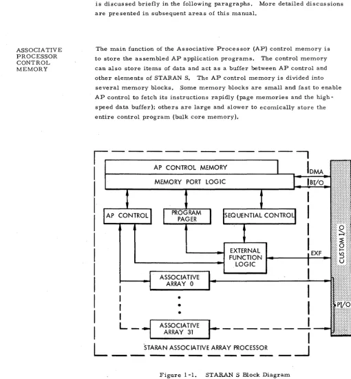
to achieve very high processing rates economically. Figure 1-1 shows
a block diagram of the STARAN S computer. Each block of the diagram
is discus sed briefly in the following paragraphs. More detailed discus sions
are presented in subsequent areas of this manual.
The main function of the Associative Processor (AP) control memory is
to store the assembled AP application programs. The control memory
can also store items of data and act as a buffer between AP control and
other elements of STARAN S. The AP control memory is divided into
several memory blocks. Some memory blocks are small and fast to enable
AP control to fetch its instructions rapidly (page memories and the
high-speed data buffer); others are large and slower to ecomically store the
entire control program (bulk core memory).
Ir...---=--==-~-
--
---=-.-I
AP CONTROL MEMORYI
MEMORY PORT lOGIC
I
I
AP CONTROl
I
I
I
I
I
I
I
L
I
I
r
I
L
ASSOCIATIVE ARRAY 0
•
•
•
ASSOCIA TlVE ARRAY 31
EXTERNAL FUNCTION
LOGIC
Figure 1-1. STARAN S Block Diagram
[image:18.615.56.567.158.709.2]ASSOCIA TIVE PROCESSOR CONTROL
ASSOC IA TIVE ARRAY MEMORY
PROGRAM PAGER
EXTERNAL FUNCTION LOGIC
SEQUENTIAL CONTROL
AP control is directly responsible for manipulation, of data within the
associative arrays under control of the program contained within the
AP control memory. Associative operations are coordinated and
controlled by AP control. Extensive interrupt and interlock capability
in AP control allow the processing capability of the arrays to be applied
quickly to an immediate requirement.
The associativ'e arrays are the heart of the STARAN S system. There
may be a maximum of 32 arrays in one system. Each associative array
contains a multidimensional-access (MDA) memory with 65,536(216)
bits of storage. A re sponse -store element in each associative array
allows array data to be searched, restructured, and processed at a
fast rate, 256 bits at a time. The array memory is arranged in a
256 -bit by 256 -bit square, with loading and storing permitted in either
the vertical or horizontal direction and with a maximum of 256 bits
transferred in a single operation. The multidimensional-access feature
allows accessing of data to take place in either dimension by simply
changing a bit in the associative instruction format.
The program pager loads the high-speed page memories from the lower
speed bulk core memory of AP control memory. The pager performs
these transfer functions independently of AP control, so that while the AP
control is executing a program segment out of one page memory, the
pager can be loading another page memory with a future program segment.
External function (EXF) logic enables the AP control, sequential control,
or an external device to control the STARAN S operation. The external
function logic facilitates coordination among the different STARAN S
elements, provides for special functions, and simplifies housekeeping,
maintenance, and test functions. By issuing external function codes to
the EXF logic, a STARAN S element can interrogate and control the status
of the other elements.
The sequential control portion of STARAN S consists of a sequential
processor (SP) having an 8K memory, a keyboard-printer, a perforated tape
reader /punch unit, and logic capability to interface the sequential processor
with other STARAN S elements. Sequential control is used for system
soft-ware programs such as assembler, operating system, diagnostic programs,
INPUT /OUTPUT VARIATIONS
STARAN S has a variety of input/output (I/O) options available. A
custom I/O cabinet containing buffered and/or unbuffered I/O channels to
data gathering. data receiving. and data-storing devices may be obtained
as part of the basic STARAN S system. STARAN S can also be integrated
with a variety of other computer systems. A direct memory access
(DMA) channel to a host-computer memory e1;lables a rapid interchange
of data between the systems in the common memory bank. A buffered
I/O channel provides an alternate means of exchanging data. while an
external function channel permits interrupts and/or other control
in-formation to be passed between the two systems.
An optional parallel input/output (PI/O) channel. with a width of up to
256 bits per array. can also be implemented in STARAN S. The extreme
width of this channel (up to 8. 192 bits). plus its submicrosecond cycle
time. gives STARAN S an I/O bandwidth many times wider than that of a
conventional computer. This PI/Ochannel can easily accommodate the
high data rates that arise in many real-time applications. Also. it
is possible for STARAN S to connect with special high-bandwidth
masstorage devices. permitting rapid retrieval, restructuring. and proces
AP CONTROL MEMORY
DESCRIPTION
General The main function of the AP control memory is to store the as sembled
AP application programs. (See figure 1-2) AP control memory can
also be used for data storage and to act as a buffer between AP control
and other elements of STARAN S. Since the AP control memory is not
an integral part of the associative arrays, AP control can overlap the
AP control memory cycle time with the associative array cycle time.
AP control memory is divided into several memory blocks. Three
small, fast memory blocks, called pages, contain the current (active)
AP program segments; the larger and slower bulk core memory block
contains the remainder of the AP program. A program pager is included
in STARAN S to facilitate transfer from the slow to the fast memory
blocks.
Each word of AP control memory contains 32 bits of either data or
instructions. Bit 0 is the left (most -significant) bit, and bit 31 is
the right (least-significant) bit of each word. Each word is given a
l6-bit address expressed in hexadecimal notation.
r-
AP CONTROL MEMORY AND MEMORY PORT lOGICI
I
I
I
PAGE 0 PAGE 1 PAG E 2
PORT SWITCH lOGIC
L ...
[image:21.612.136.542.382.674.2]DESCRIPTION
Page Memories
High-Speed Data Buffer
Three page memories are included in the AP control memory: page 0,
page 1, and page 2. Page memorie s use fast, bipolar, solid -state elements
that are volatile. Each page contains 512 words in the standard STARAN S
configuration. The page memories can be doubled to 1024 words each on
an optional basis. In the standard configuration, page 0 contains
hexa-decimal addresses 000 through IFF; page 1 contains hexahexa-decimal addresses
200 through 3FF; and page 2 contains hexadecimal addres se s 400 through
5FF.
Page 0 may contain a library of microprograms that require fast execution,
such as arithmetic subroutine s. Page s 1 and 2 can be used in ping -pong
fashion, with the AP control reading instructions out of one page while the
other is being loaded by the program pager. This permits the programmer
to use the faster memory for certain segments of the program or the entire
program if fast execution is required.
Each page memory has a port switch that connects it to one of three buses.
The port switch is controlled by external function codes. At any given time,
a page memory is connected to 1) the instruction bus, which allow s AP
con-trol to read instructions from the page; 2) the pager bus, which allows the
program pager to load the page; or 3) the sequential control bus, which allows
sequential control to read items from the page. H one of the se buse s should
try to access a word in the page memory while the port switch is set to another
bus, a hangup results. Hangups, which are detected by error detectors, cause
interrupts in sequential control.
The high-speed data buffer (HSDB), like the page memories, uses fast,
bipolar, solid-state elements and is volatile. In the standard configuration
of STARAN S it contains 512 words. As an option, its size can be doubled
to 1024 words. In the standard configuration of STAR AN S, the high-speed
data buffer contains the hexadecimal addresses 600 through 7FF.
All buses that can access AP control memory can access the HSDB making
it a convenient place to store data and instruction items that need to be
accessed quickly by the different STARAN elements.
A priority port switch on the HSDB resolves any conflict among
buses-each memory cycle is given to the highest priority bus requesting an HSDB
address at that time, while other buses requesting HSDB addresses wait for
the next memory cycle. Priorities among buses are as follows:
1) Buffered I/O bus to I/O cabin:et (highe st priority)
2) AP control data bus
3) AP control instruction bus
4) Program pager bus
DESCRIPTION
Bulk Core Memory
Direct Memory Access
ADDRESSlNG
General
The bulk core memory uses nonvolatile core storage. In the standard
configuration it contains 16,384 words (hexadecimal address 8000 through
BFFF). It is expandable to 32,768 words.
Like the high-speed data buffer (HSDB), the bulk core is accessible to all
buses that can access AP control memory (through a priority port switch
that gives each memory cycle to the highest priority bus requesting a bulk
core address). The priorities of the buses are the same as those for the
high-speed data buffer.
The bulk core memory, which is large and nonvolatile, is used for storing
the AP control programs. Because the bulk core memory is slower than
the page memories, it is recommended that program segments be moved
into the page memories for execution. Also, since the bulk core memory
is accessible to all buses having access to AP control memory, it is also
useful as a buffer for data items that do not require the high-speed of the
HSDB.
A block of AP control memory addresses is reserved for the direct
memory access (DMA) channel to external memory. In the standard
configuration this block can contain up to 30,720 addresses (hexadecimal
addresses 0800 through 7FFF). 1£ any page memory or the high-speed
data buffer is expanded, the DMA block may be reduced.
All buses accessing AP control memory can access the DMA block. A
priority port switch resolves any interbus conflicts, giving each access
cycle to the highe st priority bus reque sting a DMA addre s s at the time.
Priorities among buses are the same as those for the high-speed data
buffer.
Each AP control memory word contains either 32 bits of data or instructions.
ADDRESSlNG
Bulk Core Memory
Page Memories
High-Speed Data Buffer
• Branch and Link Registers
Change 1
The bulk core memory contains 16,384 words of memory in the standard
configuration and is expandable to 32,768 words. These words are assigned hexadecimal addresses 8000 through BFFF.
Certain words in the bulk core memory are dedicated to special purposes.
For the standard configuration of STARAN S, these locations, are as follows:
Hexadecimal Address
Use
8000
8001
First AP control instruction when activated
AP control interrupt
800F AP control interrupt 15
When the AP control becomes active, the instruction at 8000 is the first
instruction executed. It is usually a branch instruction to the beginning of
the first program segment to be executed.
The three page memories, 512 words each, that are included in the AP
control memory are de signated page 0, page 1, and page 2. In the standard
configuration, page
a
contains hexadecimal addresses 000 through IFF;page 1 contains hexadecimal addresses 200 through 3FF; and page 2 contains
hexadecimal addresses 400 through 5FF.
The high-speed data buffer contains 512 words of memory in the standard
configuration, but can be doubled to 1024 words on an optional basis. In
the standard configuration, the high -speed data buffer contains hexadecimal
addresses 600 through 7FF.
Certain words in the high -speed data buffer are dedicated to special purpose s .
These locations are used as branch and link registers to facilitate subroutine
linkage. For the standard configuration of STARAN S, the locations are as
follows:
Hexadeclmal Address
600
601
602
603
604
605
606
607
Use
Branch and Link Register
a
Branch and Link Register
Branch and Link Register 2
Branch and Link Register 3
Branch and Link Register 4
Branch and Link Register 5
Branch and Link Register 6
Branch and Link Register 7
1-7
Direct Memory Access
ASSOCIA TIVE PROCESSOR CONTROL MEMORY SUMMARY
A block of AP control memory addresses is reserved for the direct
memory access (DMA) channel to access the memory of a host
computer. This block can currently contain up to 30,720 addresses,
which are assigned hexadecimal addresses 0800 through 7FFF. This
block may be reduced if page memories or the high- speed data buffer
is increased in size.
Table 1-1 summarizes the AP control memory characteristics of the
standard configuration. The characteristics of each memory and the
connection of each bus to each section are given.
Table 1-1. AP Control Memory Characteristics
MEMORY BLOCKS
ITEM CORE PAGE 0 PAGE 1 PAGE 2 HSDB
Mag.
Implementation Core Bipolar Bipolar Bipolar Bipolar
Volatile No Yes Yes Yes Yes
Number of Words 16,384 512 512 512 512
Bits Per Word 32 32 32 32 32
First Octal Address 100000 000000 001000 002000 003000
Last Octal Address 137777 000777 001777 . 002777 003777
First Hex Address 8000 000 200 400 600
Last Hex Address BFFF IFF 3FF 5FF 7FF
Port Switch Control Priority Ext Fcn Ext Fcn Ext Fen Priority
Buffered I/O RW
-
-
-
RWB AP Control Data RW
-
-
-
RWU AP Control Instr R R R R R
S
Program Pager R W W W R
Sequential Control RW R R R RW
-
Bus cannot,access memory.R Bus can only read from :memory.
W Bus can only write into memory.
RW Bus can both read and write into memory.
? Depends on customized use of DMA.
DMA
?
?
30,720
004000
077777
0800
7FFF
Priority
RW
RW
R
R
ASSOCIA TIVE PROCESSOR CONTROL
GENERAL The major function of the AP control is to control the STARAN S associative
arrays. AP control fetche s instructions from the AP control memory. A
16 -bit program counter contains the addres s of the instruction, while a 32 -bit
instruction register contains the instruction itself. Some instructions perform
array operations, while others perform AP control functions. Internal registers
affect control operations and other elements of the hardware.
AP control consists of eight basic elements (see figure 1-3) as follow s:
1) Instruction Register
2) Program Control
3) Bus Logic
4) Common Register
5) Field Pointers and Length Counters
6) Response Store Control
7) Array 'Control
8) Reso1v'er'
I
-I
PROGRAMCONTROL
AP CONTROL
INSTRUCTION REGISTER
I
I
I
I
I
Figure 1-3
ARRAY
CONTROL RESOLVER
I
I
I
I
1
-I
~
AP Control Block Diagram
[image:26.620.63.577.145.762.2]INSTR UC TION REGISTER
PROGRAM CONTROL
Program Counter
Start Loop Marker
End Loop Marker
Comparator
Status Register
BUS LOGIC
The instruction register contains the instruction being executed. The
instruction loaded into the instruction register is received from AP
control memory via the instruction bus. Parity is checked at the
in-struction register. The inin-struction register contains 32 bits, which
are numbered from
a
to 31 with bit 0 at the left. Portions of thein-struction register are used as a direct source of data or addresses as
a function of the instruction being executed.
The sequence in which instructions are obtained from AP control memory
is controlled directly by the program control logic. The program control
logic consists of the following: the program counter, the start loop marker,
the end loop marker, the comparator, and the status register.
The program counter contains the addre s s of the instruction being read
from control memory. It is a 16 -bit counter incremented by AP control.
The program counter may be loaded from the bus logic; e. g., a branch
instruction loads an address. The contents of the program counter form
bits 0 through 15 of the program status word.
The start loop marker is used to store the address of the first instruction
immediately following a loop instruction. The start loop marker is a
16 -bit register loaded directly from the program counter at the start of
an instruction loop. It is loaded into the program counter when the last
instruction of the loop has been executed and the loop is to be repeated.
The end loop marker is used to store the addre s s of the last instruction
of a loop. The end loop marker is a 16 -bit register loaded from the
rightmost 16 bits of the loop instruction.
The comparator compares the address contained in the end loop marker
with the address in the program counter. The comparator is a full 16-bit
comparator, the output of which is transmitted to control as an indication
that the end of the loop has been reached. The control then loads the start
loop marker contents into the program counter if the loop is to be repeated.
The status register contains the interrupt mask (IMASK) for the 15 AP
control interrupts. All interrupts with number s higher than the mask are
accepted. The status register make s up bits 28 through 31 of the program
status word.
The bus logic provides a common data path for all pertinent registers of AP
control and the data bus from control memory. The bus is 32 bits wide.
Registers of less than 32 bits are grouped to form a 32 -bit word. Details
Shift Logic
Data Pointer Register
Block Length Counter
COMMON REGISTER
Change I
PORT ...
1---
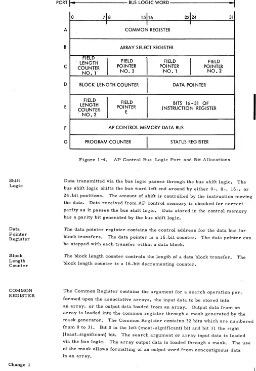
BUS LOGIC WORD - - - -...-.11
0
71s
15116 23124 31I
I
IA
COMMON REG ISTER.B
ARRAY SELECT REGISTERFIELD
FIELD
1
FIELD FIELD
LENGTH
POINTER POINTER POINTER
COUNTER.
NO.3 NO.1 NO.2
N'O:
r
C
D BLOCK LENGTH COUNTER: DATA POINTER
FIELD FIELD
BITS 16 - 31 OF
LENGTH POINTER
INSTRUCT/ON REGISTE-R COUNTER
, NO.2 E
E
F
AP CONTROL MEMORY DATA BUSG
PROGRAM COUNTERI
STATUS REG ISTERFigure 1-4. AP Control Bus Logic Port and Bit Allocations
Data transmitted via the bus logic passes through the bus shift logic. The
bus shift logic shifts the bus word left end around by either 0-, 8-, 16-, or
24-bit positions. The amount of shift is controlled by the instruction moving
the data. Data received from AP control memory is checked for correct
parity as it passes the bus shift logic. Data stored in the control memory
has a parity bit generated by the bus shift logic.
The data pointer register contains the control address for the data bus for
block transfers. The data pointer is a 16-bit counter. The data pointer can
be stepped with each transfer within a data block.
The block length counter controls the length of a data block transfer. The
block length counter is a 16-bit decrementing counter.
The Common Register contains the argument for a search operation
per-Iormed upon the associative arrays. the input data to be stored into
an array, or the output data loaded from an array. Output data from an
array is loaded into the common register through a mask generated by the
mask generator. The Common Register contains 32 bits which are numbered
from
a
to 31. Bita
is the left (most- significant) bit and bit 31 the right(least-significant) bit. The search argument or array input data is loaded
via the bus logic. The array output data is loaded through a mask. The use
of the mask allows formatting of an output word from noncontiguous data
in an array.
[image:28.612.45.551.24.756.2]COMMON' REGISTER
Mask Generator
FIELD POll'JTERS AND LENGTH COUNTERS
Field Pointer
Field Pointer 2
Field Pointer 3
Field Pointer E
Field Length Counter
The mask generator generates a mask pattern to be used in loading
array output data into the common register.
to be loaded for a number of contiguous bits.
The mask enables data
The mask generator
requires the bit addresses of the most- and least-significant bits to be
loaded. All bits between and includi.ng the se limits are loaded, while
those outside the se limits are unaltered.
Field pointers generally contain bit slice or word addresses for indirect
addressing mode in the associative array operations. The field length
counters control the number of bits to be operated on in sequence. There
are three field pointers and two field length counters. In addition, one
register for temporary pointer storage is required for the
multiply-and-divide associative instructions. A selector is used to route either field
pointers 1, 2, or 3 or the address field of the instruction register to the
array. These registers are 8 bits in length and their contents range from
o
to 255. When attempting to increment above 255, the register will returnto zero; when attempting to decrement below zero, the register contents
become 255. The field length counters can be decremented only.
Field pointer 1 may contain an array address for an associative array
operation or the address of a selected bit of the common register to be
used for a search instruction. Field pointer 1 (like field pointers 2 and 3)
is an 8-bit counter. As a result of resolve operation, field pointer 1 will
be loaded with the number of the array module containing the first responder
(i. e., first selected word whose Y flip-flop is set to one).
Field pointer 2 may contain an array address for an associative array
operation. As a result of a resolve operation, FP2 will be loaded with
the word address of the first responder in the array specified in FPl.
Field pointer 3 contains an array bit or word address.
Field pointer E is an 8 -bit counter used for temporary storage of an array
bit or word address. The register is used in the execution of the associative
multiply-and-div'ide subroutines to hold the successive starting points of the
partial products or intermediate dividends. It also may contain a shift
constant for certain associative operations.
Field length counter 1 and field length counter 2 are 8 -bit counters. The
length counters can be decremented only. When the contents of a field
counter become zero, a signal is sent to AP control for test purposes.
Field Length Counter
(cont)
Field Length Counter 2
RESPONSE STORE CONTROL
Control Line Conditioner
Control Line Buffer
ARRAY CONTROL
Array Select Register
Array Address Select
counter becomes zero. Field length counter 1 is typically used to
control the number of cycle s made for a minor instruction loop, such
as search or add fields.
Field length counter 2 may be used to control the cycles of a major
instruction loop, such as multiply fields.
The response store control logic generates the control signals required
by the associative arrays and buffers them to insure correct timing at
the response store. The re sponse store control consists of the control
line conditioner and the control line buffer.
The control line conditioner generates the control lines required to manipulate
the response store. Control line signals are generated as a function of the
instruction register, a selected bit of the Common Register and the inclusive
OR output from the resolver.
The control line buffer controls the timing of the control lines transmitted
to the associative arrays.
Control lines to the associative arrays not generated by the response store
control are generated by the array control. The array control logic select",
which arrays are to be used and controls such th.ings as bit/word mode,
store mask, and shifting.
The array select register establishes which array modules are to be enabled
for an operation. The array select register is 32 bits wide. Each bit
position controls one array. Bit 0 corresponds to array 0, and a 1 in
a bit position enables the corresponding array. The array select register
contents are also used by the resolver logic.
The array addre s s select logic selects either the array select register
or field pointer 1 to generate the array enable signals. When field pointer
is selected, the five right-most bits of the pointer specify the one array
to be enabled. This is done without modifying the contents of the array
select register. Such operations as loading one item of data from
at). array or storing one item of data into an array enables only one of the
associative arrays. When more than one array is involved in an operation,
ARRAY
CONTROL
Array Mode
Shift Control
RESOLVER
The array mode logic controls the addressing mode. Either a bit slice
or a word slice in the arrays is selected for loading or storing.
The shift control logic generates the control signals required by the
array to perform shifting and mirroring operations.
The resolver logic finds the array address and word address of the first
(most-significant) responder. A responder is a response store element
in an enabled array whose Y flip-flop is set to one. Generally,
responders indicate those words satisfying some search criteria. The
array address is loaded into field pointer 1 and the word address is
loaded into field pointer 2. This allow s subsequent operations to affect
ASSOCIATIVE ARRAYS
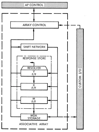
GENERAL DESCRIPTION
Change 1
Each STARAN arraY(see figure 1-5) includes a 256 -word by 256 -bit
square array of solid-state multidimensional access (MDA) storage.
Associated with each word of an array is a three flip-flop response
store element (M,X, and Y registers). Also included in each array is
a network to facilitate data manipulation and interword communication,
a 256-bit widePI!Oport communicating with the custom I/O unit, and
dual control ports to allow processing in some arrays concurrently with
input/output in other arrays.
I
I
I
I
I
I
I
I
I
I
I
I
L
ARRAY CONTROL
SHIFT NElWORK
I
RESPONSE STORE-l
I I
ASSOCIATIVE ARRAY
~---Figure 1-5. Associative Array Block Diagram
I
[image:32.612.199.523.239.668.2]GENERAL DESCRIPTION (cont)
ADDRESSING
Arrays
Words
Bit Columns
The associative array consists of two basic components, the array
storage and the response store. As many as 32 associative arrays may
be contained within one system. Arrays may be selected and operated
in parallel or one at a time.
Each array contains 65,536 bits, organized as a square .256 words by
256 bits of solid-state storage. By use of a special organization within
the array, access may be made in either the bit or word direction. An
entire word of 256 bits or a bit slice, bit n of all 256 words, may be
accessed.
The response store portion of the array consists of 256 response store
elements. The M, X, and Y response store registers (256 bits each)
may be used as temporary storage of data loaded fro:m the array or :may
contain the data to be stored into the array. The X and Y registers :may
also logically combine array data simultaneously with the load response store
operations. The M (MASK) register is used as a MASK to select which
words of array memory participate in an array Store Operation.
The Y register is used as a responder by the resolver in a search type
operation.
Associative array input and output may be either 32 bits (via the co:mmon
register) or 256 bits (via the response store registers or Parallel I/O
if the PI/Ooption is selected).
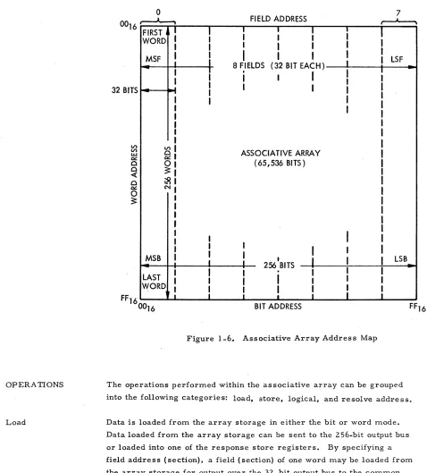
Addressing of and within the associative arrays is carried in hexadecimal
notation. The four basic areas to be addressed are arrays, words, bit
columns, and fields. (See figure 1-6)
Addressing of arrays is accomplished by an address from O. the first array,
to 31, the last array. The number of arrays within a system, therefore,
ranges from 1 to 32 as dictated by the requirement placed on the system.
The internal organization and addressing of all arrays are identical.
Addressing of a word within an array is accomplished by an address
from 0, the first word, to 255, the last word. An array word consists
of 256 bits, all of which may be accessed in parallel or divided
into eight fields of 32 bits each and accessed via the Common Register.
Addressing of a bit position within an array is accomplished by an
addres s from 0, the mos't-significant (left), to 255, the
least-significant (right) bit position. Bit (n) of all words is acces sed
ADDRESSING
Fields
OPERATIONS
Load
Addressing of a particular field of an array word is accomplished by an
an addre ss from 0, the most -significant (left) field, to 7, the
least-significant {right} field. Each field contains 32 contiguous bits within
the word being addres sed. The m.ost -significant field starts at the
most -significant bit position.
32 BITS
V) V)
w
0:::
o
o
«
o
0:::
o
3:
.
o
FIRST WORD
MSF
V) 0
0:::
0
3:
1R
N
MSB
LAST WORD
.
I
I
I
I
I
I
I
.1
-,
.
I
FI ELD ADDRESS 7
:
;
II
;
I
I
I
I
II
I
I
I
I
I
I
I
I
I
I
I
LSF8 FIELDS (32 BIT EACH)
;
,
I
I
II
I
I
I
I
I
I
I
I
I
I
ASSOCIATIVE ARRAY (65,536 BITS)
I
I
I
I
I
I
I
I
II
I
LSBI I 256 BITS
I
I
1
I
I
I
I
I
I
I
:
!
!
:
IBIT ADDRESS
Figure 1-6.. Associative Array Address Map
The operations performed within the associative array can be grouped
into the following categories: load, store, logical, and resolve address.
Data is loaded from the array storage in either the bit or word mode.
Data loaded from the array storage can be sent to the 256-bit output bus
or loaded into one of the response store registers. By specifying a
field address (section). a field (section) of one word may be loaded from
the array storage for output over the 32 -bit output bus to the common
register. Also, one response store register may be loaded with the contents
of another response store register. All loads from the array storage are
nondestructive. Logic may be performed between the X and Y registers
[image:34.612.75.553.163.692.2]OPERATIONS
Masked Store
Logical
Resolve
Data is stored into the array mem.oryin either the bit or word mode.
The data, regardless of source, may be stored through a mask
contained in the M response store register. Data to be stored may come
from the response store registers, the 32-bit input bus, or the 2s6-bit
input bus (parallel I/O).
To perform operations such as exact -match search and add fields,
certain logical operations must be performed on the data in the
response store registers. Data loaded from the array memory may
be logically combined with the current contents of the response
store to accomplish these operations. Data may also be transferred
am.ong the response store registers with logic functions applied
to the X and/or Y registers.
The array address and bit or word address of the first Y response store
element set is continuously resolved. This addres s and the inclusive OR
of all Y response store elements are made available to control. This
address (which is stored in FPl and FP2) may be used in succeeding
PROGRAM PAGER
GENERAL The function of the pr,ogram pager is to transfer program segments
from the bUlk core memory to the page memorie s.
Under normal programming practice, the pager is activated by AP
control when a new program segment is to be transferred to a page
memory. The program pager transfer s the segment one word at a
time at a rate dictated by the source memory. while AP control executes
instructions from previously loaded segments. When the pager completes
the transfer, it restores the page memory port switch to the AP instruction
bus and halts.
The program pager contains three registers. (See figure 1 -7.) The GET
address register contains a 16-bit AP control memory address. If the pager
is in the midst of moving data, the GET address points to the memory
location containing the next source word to be moved. At other times the GET
address acts like a program counter, pointing to the location of the next
page memory instruction to be executed.
I
I
I
I
I
I
PUT REGISTER (16 - BIT)
I
L
PAGER CONTROL
WORD CENTER (16 BIT)
PROGRAM PAGER
I
I
I
I
I
_.J
[image:36.615.66.575.87.738.2]GENERAL (cont)
OPERATION
The PUT address register holds a 16-bit AP control address. It points
to the memory location into which the next destination word is to be put
during a move-data operation.
The 14-bit count register holds the number of words still to be transferred
during a transfer operation.
Pager transfer speed is governed by the cycle time of the source memory,
which can be slower than AP control execution speed. To keep STARAN
from being "pager bound:' AP programs should be segmented carefully.
An ideal program segment will contain enough long instructions, subroutine
calls and loops, etc., so that before AP control leaves the segment, the
pager has had enough time to get the next segment loaded in a page memory.
If all segments are ideal, AP control will never wait for the pager.
Each page memory has a port switch to pre vent AP control from jumping
into a segment before the pager has loaded it. A premature attempt to
jump into a page memory that is still being loaded by the pager will be delayed
until the pager has switched the port switch to the instruction bus.
Pager operation is initiated by an external function code that loads the GET
address register. With one external function code the current pager operation
can be stopped in midstream and a new operation started. For instance,
suppose from program segment 1, AP control either jumps to program segment
2 or to program segment 3, depending on some condition. Most of the time it
jumps to segment 2. In this case, AP control can initiate the loading of
segment 2 as it begins executing segment 1, so that little or no time is lost in
waiting for the pager. In the rarer case, when AP control jumps to segment
3, it can stop the loading of segment 2 in midstream, if neces sary, and start
the loading of segment 3.
When the program pager is running (busy), it fetches pager commands and
source data from AP control memory. Its commands are sufficiently general
EXTERNAL FUNCTION LOGIC
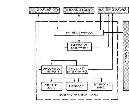
GENERAL Numerous hardware functions are under the control of external function
(EXF) logic. These include page memory port switches, AP and
sequential control interrupts, AP control and program pager activity
control, and resets and clears. Control and status sensing of these
functions are accomplished by issuing 19 -bit external function commands
to EXF logic and receiving one -bit sense signals in return. Three
elements of the main frame can issue EXF commands: AP control,
program pager, and sequential control. (See figure 1-8.)
EXF logic is expandable to allow receipt of EXF commands from the
custom I/O unit and control of other hardware functions in the custom
I/O unit. A resolver in EXF logic allows only one EXF command
to be treated at a time.
The resolver in EXF logic resolves conflicts among the four elements
issuing function codes. One function code at a time is accepted by EXF
AP CONTROL INTERRUPTS
MISC EXF LOGIC
EXF SELECT FAN-OUT
EXF RESOLVE PORT SWITCH
ERROR SEQ
INTER CONTRO
INTERLOCKS INTERLOCK PANEL