explanations for a contrast reversal effect in between s- and p-polarized light are given. One is based on the excitation of a quasi-transverse electric and magnetic mode in the mesoscopic transmission line. For this explanation we have made a prediction of the condition of the maximum coupling efficiency through the approach of impedance matching. The second explanation is based on surface plasmon excitation in the gold structure. The present results can also be of importance in the development of new concepts of probes for SNOM. © 2004 American Institute of Physics. 关DOI: 10.1063/1.1649453兴
I. INTRODUCTION
The study of electromagnetic coupling into small metal structures is motivated by fundamental research and also by possible applications of the optical properties of such struc-tures. In the case of coupling of light from a probe of a scanning near-field optical microscope共SNOM兲into a metal structure there is additional interest driven by the issues of understanding the mechanisms of the contrast formation, contrast polarization dependency, and also by the interest of developing more efficient SNOM probes. In the case of cer-tain metals like gold and silver showing significant plasmon resonance efficiency, there is a further issue of understanding the contribution of plasmons into the optical properties of the structure. For example, squeezing of the optical near-field due to plasmon coupling was observed above a chain of Au particles.1 The preset experimental study aims at achieving improved understanding of the coupling of light from a fiber probe of a scanning near-field optical microscope to a meso-scopic metal structure. In particular, we focus on the issues of the dependency of coupling on the polarization of light at the output of the probe and the size of the structure.
The metal structure consisting of parallel metal lines de-posited on a dielectric substrate is a convenient model struc-ture due to its simplicity and also due to expected significant dependency of the optical properties of the light polarization. Optical response of periodic arrays of metal and dielectric lines has been modeled theoretically.2Strong polarization de-pendency of optical properties of Au nanowire grating in the far field was observed by Schider et al.3
We performed the experiment using scanning near-field optical microscopy 共SNOM兲,4 a technique which allows resolution well below the diffraction limit. The key element of the technique is a probe, usually consisting of a tapered optical fiber coated with metal to form an aperture of the size 30–150 nm at the end. The probe forms a localized light source, illuminating only the part of the sample close to the aperture. When using polarized light it is therefore possible to study the effect of the light on the sample and sample structure, depending on the polarization direction, close to the aperture. This was shown using magnetic samples with magneto optical Kerr effect.5
It is well appreciated that more commonplace accep-tance of SNOM as a measurement technique depends on de-velopment of new probes capable of better resolution and more straightforward image interpretation. The work on new SNOM probes has received much attention from the near-field optics community.6,7
II. EXPERIMENT
The instrument used for the experiment is a reflection-mode SNOM. The collection of the light is performed by an elliptical mirror.8 –10The probe/sample interface is located at the first focal point, while the light is collected by a photo-multiplier tube共PMT兲located at the second focal point. The optical layout can be seen in Fig. 1.
The probes are produced by tube etching proposed by Stockle et al.11They are coated to have⬃40-nm-thick alu-minum film at the tip apex forming an aperture at the very end of the tip. The laser used is a 635 nm diode laser. The light coming from the tip can be polarized by using a quarter wave plate and a half wave plate. The polarization is
mea-a兲Author to whom correspondence should be addressed; electronic mail: [email protected]
3988
sured by placing an analyzer in between the probe and the PMT and it could be chosen in the range of 1:1–1:20 with alignment along any desired direction.
Two types of samples were produced by e-beam lithog-raphy. They consisted of gold lines, 20 nm thick and 1000 nm wide, formed on a silicon substrate. The distance be-tween the lines is 250 nm for sample 1 and varies regularly between 200 and 1000 nm for sample 2. The area between the lines is the bare silicon substrate.
Due to the high confinement of light in the aperture re-gion of the probe, a distance feedback mechanism is required to maintain the sample within the near field of the aperture. The technique used here was shear-force detection,12,13 which allows us to simultaneously共1兲image the sample to-pography and共2兲obtain SNOM images. The probe could be kept at a constant height of 5–30 nm above the sample, with the accuracy of ⫾2 nm using the shear-force feedback sys-tem described in Ref. 14.
[image:2.612.332.548.48.405.2]III. RESULTS
Figure 2 shows two optical SNOM images of a 4m⫻4 m area of sample 1. Figure 2共a兲is recorded with light po-larized parallel to the Au lines 共TM polarization兲 and Fig. 2共b兲 with light polarized perpendicular to the lines 共TE po-larization兲. An analyzer was not used in these experiments.
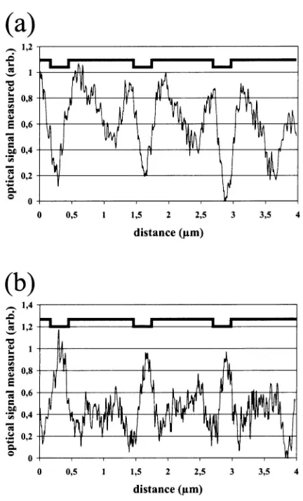
Particles of dust identifiable on both images indicated that they were taken at the same area of the sample. Figure 2共a兲 shows the line as bright and the gap as dark, while Fig. 2共b兲 shows the line as dark and the gap as bright. When only material reflectivity is used to interpret the images, Fig. 2共a兲 can be explained, taking into account that the reflectivity of gold is higher compared to silicon. But Fig. 2共b兲could not be explained. When comparing the actual measured intensities, taken as an average on top of the Au lines, it shows that the intensity change in between the two polarization directions is approximately 10%. Whereas if the mean values measured in between the lines are taken, a change of polarization results in an intensity change of up to 70%. This can be seen in the profiles共Fig. 3兲taken at the representative cross-section AA
⬘
of Fig. 2. [image:2.612.71.276.54.223.2]For details of interpretation of the results presented in Figs. 2 and 3 we refer the reader to our earlier publications.8,10 These publications deal with the contrast formation in a reflection-mode SNOM and dependency of the contrast on the polarization of light. The test samples employed in the studies8,10are rather similar to the ones used in this study: metal stripes deposited on a dielectric substrate. There were two substantial differences. First, in Refs. 8 and 10, unlike in some of the samples used in the present study,
FIG. 1. Schematics of the optical layout of the reflection mode SNOM.
FIG. 2. Scans of the same area of the sample taken with polarization along the transmission line structures共TM polarization兲 共a兲and perpendicular to them共TE polarization兲 共b兲. Arrows indicate the polarization directions used for the respective images.
FIG. 3. Representative cross sections taken at the lines AA⬘marked in Figs.
[image:2.612.78.272.600.711.2]contrast is reversed. The contrast reversal takes place due to the increase in measured intensity from the areas in between the Au lines. The contrast reversal is due to more efficient coupling of light with such a perpendicular polarization from the probe to the structure. In the case of perpendicular polar-ization, a transverse electric and magnetic 共TEM兲 mode is launched when the probe is placed in between the Au lines, whereas it cannot be launched in the case of longitudinal polarization. Fully in line with conclusion of Refs. 8 and 10 we now observe that the signal intensity above the metal lines is mainly not polarization sensitive, but the one above the Si substrate in between the lines is.
Two possible explanations could be taken into account here. The first explanation models each pair of the nearest gold stripes as a transmission line. Such a transmission line can support TE mode with the polarization directed perpen-dicular to the lines. On the contrary, for the TM polarization the transmission line cannot support the mode. As a result the light cannot be efficiently coupled into the structure and therefore it is reflected back into the SNOM probe.
The second explanation is based on the local excitation of surface plasmons in the gold surface. The plasmon propa-gation direction is dependent on the polarization of the ex-citing light. Results of the letter in Ref. 15 suggest that gen-erally plasmons propagate along the probe polarization direction. When the surface plasmon propagates to an edge boundary of a gold stripe it can scatter and reemit light which can then be detected with the PMT. As a result, an image taken with TE polarized light should show enhanced light detected at the edges next to the gaps.
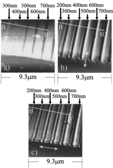
Figure 4 shows topography and the optical SNOM im-ages of a 9.3m⫻9.3m area of the second sample. Figure 4共a兲is the shear-force image of the sample and Figs. 4共b兲and 4共c兲are the optical images with the main axis of polarization parallel and perpendicular to the lines, respectively. The same dust particles identifiable on all three images indicate that the scans are all taken at the same area. The tip used for this experiment had an approximate aperture of 150 nm, as confirmed by scanning electron microscope for probes pro-duced in the same way. An analyzer was not used in this experiment. Optical results presented in Figs. 2 and 4 with the same direction of polarization compare well. Once the polarization direction is set perpendicular to the lines 共TE polarization兲 an increase in signal intensity in the gaps be-tween the gold lines is observed compared to the images
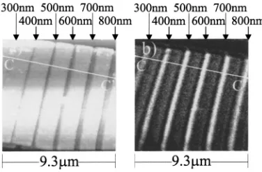
[image:3.612.342.530.48.327.2]measured with parallel polarized light 共TM polarization兲. Figure 5 shows this in the representative cross section. How-ever, there is an additional feature in the result shown in Fig. 4. As the gap gets wider from 200 to 400 nm, the intensity of the optical signal measured at the gap intensity increases and then with, further increase in the gap width, it decreases pro-vided the polarization is TE. The maximum/minimum com-bination visible on the right hand side of the gap and the left hand side of the lines in both optical images of Fig. 4 is most likely due to shadowing effects and a not totally symmetric collection of the light. Due to the fact that this minimum/ maximum combination is independent of the polarization di-rection it does not contribute to the effect described here. Similar observation was made by us in Refs. 8, 10, and 16. Figure 6 shows topography and optical SNOM images of a 9.3 m⫻9.3 m area of the second sample. Figure 6共a兲 shows the shear-force image of the sample and Fig. 6共b兲 shows the optical image taken with polarization perpendicu-lar to the gold lines共TE兲. The same dust particles identifiable on both images indicate that the scans are taken at the same area, and they can also be identified in the images of Fig. 4 showing the relation between the images. The tip used for these scans had an aperture larger than the one used for the previous scans. It was in the range of 180–200 nm. Compar-ing Figs. 4共c兲and 6共b兲 shows the same general characteris-tics of a higher intensity in the gaps and a change of intensity depending on gap width provided that TE polarization was used. In Fig. 6共b兲though the maximum intensity is observed when the gap width is 600 nm compared to 400 nm in Fig. 4共c兲. This is shown by the line cross-section共see Fig. 7兲.
IV. DISCUSSION
In our view the results could be explained using two different approaches. The first one is based on microwave theory. In microwave theory, a clear distinction is made be-tween transmission lines and waveguides.17 Transmission lines consist of two or more conductors separated by a
di-electric. They are able to support transverse electric and magnetic 共TEM兲 modes or quasi-TEM modes, without any cutoff frequency. Waveguides are generally represented by a metal tube of circular, rectangular, or other cross section filled with a dielectric. They cannot support a true TEM mode, in which both field vectors E and H are perpendicular to the propagation direction. Instead they support TEmn
共transverse electric兲 or TMmn 共transverse magnetic兲 modes
with only electric or magnetic field vector perpendicular to the waveguide axis, respectively. Each mode of a waveguide is characterized by its cutoff frequency.
The efficiency of electromagnetic coupling from waveguides to transmission lines depends upon the polariza-tion direcpolariza-tion in the waveguide with respect to the transmis-sion line axis,18and on the characteristic impedances of both structures. The concept of impedance matching is commonly used in the radio- and microwave frequency range. In the optical frequency range impedance matching is much more difficult to demonstrate due to the submicron size and the difficulties with fabricating the optical structures required for such experiments. The notion of optical impedance is rarely used.
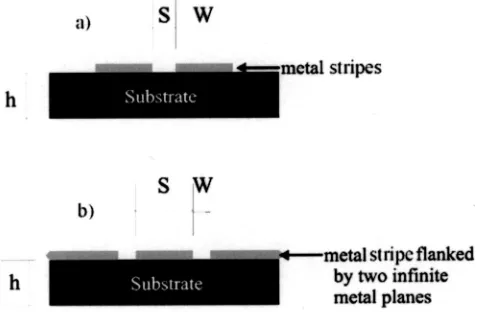
It should be noted that each pair of Au lines forms a coplanar transmission line. It can be modeled as a coplanar strip transmission line 关Fig. 8共a兲兴 or a coplanar waveguide 关Fig. 8共b兲兴. To get an approximate idea of the impedance, value formulas from microwave textbooks were used, which should give an indication of the values. The analytical ex-pression for the impedance Z019 for the coplanar stripline is
Z0⫽120•
冑
⑀eK共k兲
K共k
⬘
兲. 共1兲Impedance of the coplanar waveguide is
Z0⫽ 30•
冑
⑀eK共k
⬘
兲 [image:4.612.333.538.55.226.2]K共k兲 . 共2兲
FIG. 5. Representative cross section taken at the lines BB⬘marked in Fig. 4 for TM polarization关5共a兲兴and TE polarization关5共b兲兴. The thin lines of Figs. 5共a兲and 5共b兲represent optical intensity signals for TM and TE polariza-tions, respectively. The thick lines represent topography of the structure as position reference.
[image:4.612.70.275.58.413.2]FIG. 6. Scans of the same area of sample 2. 共a兲Shear-force topography image and共b兲an optical image taken with light polarized perpendicular to the stripes.
[image:4.612.79.267.597.721.2]Here⑀eis the effective dielectric constant, that is dependent
on the dielectric constant of the substrate and the dimensions of the structures. K(k)/K(k
⬘
) is only dependent on the di-mensions of metal structures.Using these expressions for the dimensions of sample 1 predicts an impedance of 106 or 64⍀using formulas共1兲and 共2兲, respectively. Table I shows the prediction for sample 2 taking formulas共1兲and共2兲. Due to the nature of the sample used, consisting of an array of parallel lines, none of the two models describes the impedance value accurately. This can be seen in Fig. 8. While coplanar stripline consists of two parallel lines without any other conductor in the vicinity, coplanar waveguide consists of one line with infinitely large planes left and right of it. Therefore the real impedance value should be in the range between the values calculated using formulas 共1兲and共2兲.
When the electric field from the tip is perpendicular to the line共TE polarization兲, a quasi-TEM mode can be excited in the transmission line. This is the dominant mode of this structure and does not have the limitation of a cutoff fre-quency. It results in an enhanced coupling of energy from a probe into the line structure. When the electric field from the probe is parallel to the lines共TM polarization兲no quasi-TEM mode can be excited. In the first case light gets through sub-wavelength size aperture of the SNOM probe more effi-ciently and in the second, its greater fraction is reflected back into the probe.
A mode similar to TE11 is expected to be excited at the
closer to the one of the coplanar waveguide model which is intuitively clear.
Figure 6 shows the maximum intensity at the 600 nm gap size. Table I suggests an impedance value of 133 or 82 ⍀. As impedance is greater at 600 nm separation than at 400 nm, one can expect that the impedance of the SNOM probe in Figs. 6 and 7 is greater than in Figs. 4 and 5. This is consistent with our indication that the probe in Figs. 6 and 7 had a greater aperture. Using the values of Table I we can estimate a 25% larger aperture.
The second possible explanation is based on the excita-tion of a localized surface plasmon in the gold lines. The surface plasmon can only be detected when scattered at a surface defect, as described before by Hecht et al.15Surface plasmons on gold are much stronger damped when propagat-ing along the surface compared to plasmon excited in silver. Therefore it is only possible to detect the surface plasmon when the tip is located close to the line edges. The propaga-tion of the surface plasmon is along the direcpropaga-tion of the elec-tric field. This approach may explain the increased intensity of the signal in the vicinity of the line edges and its depen-dence on the light polarization. When the light is TM polar-ized the surface plasmon will propagate parallel to the line edges and as a result its scattering is hampered. If the light is TE polarized the surface plasmon will propagate perpendicu-lar to the lines and will scatter when reaching the line edge. The change of the intensity at the sample with the chang-ing gap width could be explained by the generation of a resonance of the surface plasmon in between the edges of the two lines in the gap. This could explain the maximum inten-sity for a particular gap width.
V. CONCLUSIONS
We have presented an experimental study of coupling of polarized light to a mesoscopic metal structure containing Au lines deposited on a Si substrate with varying separation be-tween the lines. We have demonstrated an enhancement of coupling when the polarization direction at the probe is per-pendicular to the line edges on the condition that the probe is located in between the lines. On the contrary, the coupling in the case when the probe is located above the metal lines is polarization independent.
The intensity of the enhancement varied depending on the gap width and the tip used reaching the maximum for the
[image:5.612.57.297.55.211.2]FIG. 8. Sketch of cross sections of a single coplanar stripline 共a兲 and a single coplanar waveguide共b兲. Coplanar stripline consists of two parallel individual metal stripes. Coplanar waveguide consists of a single metal stripe positioned in between two infinitely large metal areas left and right of it. The two areas have their edges parallel to the stripe.
TABLE I. Impedances for sample 2.
Gap width, S nm
Coplanar stripline impedance,⍀
Coplanar waveguide impedance,⍀
200 100 60
300 111 67
400 120 73
500 127 77
[image:5.612.52.300.671.756.2]width of 400 or 600 nm depending on the used tip. We gave two possible explanations for this effect, one based on the coupling of light from a circular waveguide into a submicron size optical transmission line and the second one on the ex-citation of localized surface plasmons.
Using the first approach we could demonstrate that the coupling efficiency depends on the direction of polarization and on the condition when a quasi-TEM mode is launched in the transmission line we observe a substantial enhancement of the coupling efficiency. We have made a prediction for the condition of the maximum coupling efficiency through the approach of impedance matching. By using a sample with various impedance values imaged with probes of different apertures we demonstrated that these predictions hold well, at least semiquantitatively. The values for the optical imped-ance obtained using the standard microwave formulas must be taken cautiously as in the case of the submicrometer-size structures the skin depth becomes comparable to the size of the transmission line itself. Nonetheless, the concept of op-tical impedance matching in our view is still valid. In es-sence it states that the coupling of electromagnetic waves between two structures is maximized when the pattern of electric and magnetic field in one of them matches the same in the other.
The second explanation is based on the excitation of surface plasmons in Au lines. The plasmons propagate in the direction of electric field and scatter at the edges of the metal lines. As a result they can be optically detected.
We believe these results can be of importance in the development of new concepts for high resolution optical im-aging by means of SNOM. Samples with variable separation between the lines could be used as test samples to identify the size of the aperture at the tip. It also shows that results depend on tip 共polarization, extinction ratio, and aperture size兲, type of sample共transmission line structures兲, and the interaction between both. Possibly this could lead to a probe that is not designed as a waveguide but rather as a submicron transmission line, which could provide better extinction ra-tios. There are recent theoretical and experimental works on
the development of nonconventional SNOM probes offering higher light throughput. For example, coaxial SNOM probe was modeled in Ref. 20. In experimental study,21 massive increase in the throughput was observed for HE11 mode in a new triple-tapered probe.
ACKNOWLEDGMENTS
The authors would like to acknowledge the funding
by the EU under the TMR-project NanoSNOM
共ERBFMRXCT98-0242兲, Magnetude Project 共 G5RD-CT-1999-00005兲and by Science Foundation Ireland.
1
J. R. Krenn, A. Dereux, J. C. Weeber, E. Bourillot, Y. Lacoute, J. P. Goudonnet, G. Schider, W. Gotschy, A. Leitner, F. R. Aussenegg, and C. Girard, Phys. Rev. Lett. 82, 2590共1999兲.
2O. Keller, M. Xiao, and S. Bozhevolnyi, Surf. Sci. 280, 217共1993兲. 3
G. Schider, J. R. Krenn, W. Gotschy, B. Lamprecht, H. Ditlbacher, A. Leitner, and F. R. Aussenegg, J. Appl. Phys. 90, 3825共2001兲.
4P. W. Pohl, W. Denk, and M. Lanz, Appl. Phys. Lett. 44, 651共1984兲. 5C. Durkan, I. V. Shvets, and J. E. Lodder, Appl. Phys. Lett. 70, 1323
共1997兲. 6
A. Naber, D. Molenda, U. C. Fischer, H. J. Maas, C. Hoppener, N. Lu, and H. Fuchs, Phys. Rev. Lett. 89, 210801共2002兲.
7A. Bouhelier, J. Toquant, H. Tamaru, H. J. Guntherodt, D. W. Pohl, and G.
Schider, Appl. Phys. Lett. 79, 683共2001兲. 8
C. Durkan and I. V. Shvets, J. Appl. Phys. 83, 1171共1998兲. 9C. Durkan and I. V. Shvets, Ultramicroscopy 61, 227共1995兲. 10C. Durkan and I. V. Shvets, J. Appl. Phys. 83, 1837共1998兲.
11R. Stockle, C. Fokas, V. Deckert, R. Zenobi, B. Sick, B. Hecht, and U. P.
Wild, Appl. Phys. Lett. 75, 160共1999兲. 12
E. Betzig, P. L. Finn, and J. S. Weiner, Appl. Phys. Lett. 60, 2484共1992兲. 13R. Toledo-Crow, P. C. Yang, Y. Chen, and M. Vaez-Iravani, Appl. Phys.
Lett. 60, 2957共1992兲.
14R. Kantor, M. Lesnak, N. Berdunov, and I. V. Shvets, Appl. Surf. Sci. 145,
510共1999兲. 15
B. Hecht, H. Bielefeldt, L. Novotny, Y. Inouye, and D. W. Pohl, Phys. Rev. Lett. 77, 1889共1996兲.
16A. Gademann, C. Durkan, and I. V. Shvets, J. Phys. D 36, 2193共2003兲. 17K. F. Sander, Microwave Components and Systems 共Addison–Wesley,
Reading, MA, 1987兲.
18K. Chang, Handbook of Microwave and Optical Components共Wiley, New
York, 1989兲, Vol. 1.
19K. Chang, in Ref. 18, Vol. 1, chap. 1.3.
20
O. Rudow, A. Vollkopf, M. Mueller-Wiegand, G. Georgiev, and E. Oester-schulze, Opt. Commun. 189, 187共2001兲.