International Journal of Emerging Technology and Advanced Engineering
Website: www.ijetae.com (ISSN 2250-2459, ISO 9001:2008 Certified Journal, Volume 6, Issue 11, November 2016)
19
Timing and Power Optimizaion Using Mixed-Dynamic-Static
CMOS
Hao Xue
1, Chien-In Henry Chen
2 1,2Department of Electrical Engineering, Wright State University, Dayton, Ohio, USA
Abstract—An effective approach to timing and power optimization for single clocking and multiple clocking dynamic CMOS designs is presented in this paper. Two benchmarks are introduced to validate this theory. In comparison with the benchmark 16-bit carry-select-adder in dynamic CMOS, the critical path delay is reduced by 41.1% using the single-clock optimization technique; the power and delay are reduced by 43% and 41.1% respectively using the multiple-clock optimization technique. In comparison with the benchmark 64-bit binary comparator in dynamic CMOS, the critical path delay is reduced by 49% using the single-clock optimization approach; the power and delay are reduced by 43.1% and 49% respectively using the multiple-clock optimization approach.
Keywords—carry-select-adder, 64-bit binary comparator, mixed-dynamic-static CMOS, power and timing optimization.
I. INTRODUCTION
Circuit operation at high frequencies while consuming low power is one of the most important characteristics in designing integrated circuits (ICs). Compared with static CMOS circuits, dynamic CMOS circuits are faster by reducing load capacitance; however dynamic circuits have higher power consumption due to the operating mechanism. The high speed of dynamic circuits resulted in this class of circuits having an important role in the high performance digital IC market. But in recent years, the power hungry dynamic ICs are becoming a heavy load for battery and heat dissipation demands in portable IC products. Researches introduce timing and power optimization in past decades [1][2][3]. However, most of these studies are in gate level that is only suit to specific circuitry, [4] is aware of structure level optimization that could expand to most chip designs. Author in [4] introduces a transistor level optimization algorithm for timing. However, [4] scarcely show the implementation dynamic or static logic for timing optimization. This paper introduces an effective approach to optimize timing and power by mixed-static-dynamic CMOS logic that can be applied to general circuit design.
II. PRELIMINARIES
In this section we present a brief overview of basic CMOS logic circuit design that we will use in this paper. It includes static, dynamic, and mixed-dynamic-static CMOS logic in single- and multiple-clocking circuit.
Comparing with static CMOS, the dynamic CMOS is fast and area-efficient, but it consumes more power as tradeoff. Its high speed, which is one of the foremost characteristics in integrated circuit (IC) design, has led it to play important role in the high performance digital IC market. Thus dynamic CMOS logic using NMOS pull down network is preferred for smaller silicon area and lower power [6][7][8][9][10][11][12].
As seen in Fig. 1, the dynamic circuit has two operation phases: pre-charge and evaluation, controlled by the clock Φ. During the pre-charge phase, Φ is low; the PMOS M1 is turned on and the NMOS M2 is turned off. The output is pulled up to the high voltage (logic ‗1‘) through the PMOS M1. In the evaluation phase, Φ is high; the PMOS M1 is turned off and the NMOS M2 is turned on. Then the output is pulled down to the low voltage (logic ‗0‘) if the NMOS pull-down network is on. Otherwise, the output stays at high voltage (logic ‗1‘) [5].
As shown in
International Journal of Emerging Technology and Advanced Engineering
Website: www.ijetae.com (ISSN 2250-2459, ISO 9001:2008 Certified Journal, Volume 6, Issue 11, November 2016)
20
NMOS logic
Φ
inputs
output
Φ
M2 M1
[image:2.612.64.267.126.270.2]pre-charge evaluation pre-charge
Fig. 1 Single-clocking half-time dynamic CMOS structure
NMOS logic A
Φ
inputs
M2 M1
NMOS logic B
Φ
inputs
output
M4 M3
Stage 1 Stage 2
Φpre-charge evaluation pre-charge
Fig. 2 Full-time dynamic CMOS structure
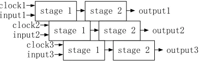
Multiple-clocking dynamic CMOS is used to speed up full-time dynamic CMOS. As shown in Fig. 3, multiple clocks control multiple dynamic CMOS circuits operate in parallel. The next input data can be applied and evaluated without waiting for the previous input data propagation. The data throughput is therefore increased.
stage 1 clock1
input1 stage 2 output1
stage 1 clock2
input2 stage 2 output2
stage 1 clock3
[image:2.612.60.279.293.403.2]input3 stage 2 output3
Fig. 3 Multiple-clocking dynamic CMOS structure
In addition to clock pulse, the delay of data for being used (data efficiency) needs to be considered for timing and power optimization. The clock pulse and data delay in a full-time dynamic CMOS is demonstrated in Fig. 4. As long as the delay is maintained, the clock pulse can be optimized for power reduction if the timing requirement is met.
precharge evaluate precharge evaluate precharge Stage 1 Stage 2 Stage 1 Stage 2
Evaluate-time for stage 1 Evaluate-time for stage 2
Clock
pulse Delay
Fig. 4 Clock pulse and delay of full-time dynamic CMOS operation
III. TIMING AND POWER OPTIMIZATION ALGORITHM
As discussed in section II, in CMOS logic, full-time dynamic CMOS is fastest design, yet either static CMOS or mixed-dynamic-static CMOS can be applied to replace dynamic CMOS logic for power reduction. To show our methodology for balancing power and timing, two cases of CMOS operation are shown in Fig. 5 for analysis. In Case I, the delay of stage1 is close to that of stage2. Using single-clocking dynamic CMOS, no resource can be optimized for power reduction; timing optimization stays focused. Using multiple-clocking dynamic CMOS, the delay for data use can be applied as trade-off to reduce power. For example, replacing the stage1 of dynamic CMOS with a static CMOS or a mixed-dynamic-static CMOS. In Case II, the delay of stage1 is greater than that of stage2. Using the single-clocking dynamic CMOS, if timing is prior to power then the full-time dynamic CMOS should be chosen. However, if power is prior to timing then the free time in the stage2 can be utilized for power reduction, by replacing the stage2 with a static CMOS or a mixed-dynamic-static CMOS. Using the multiple-clocking dynamic CMOS, the clock pulse can be optimized for power reduction, by replacing the stage2 by static CMOS or mixed-dynamic-static CMOS.
precharge evaluate precharge evaluate precharge
Stage 1 Stage 2 Stage 1 Stage 2
precharge evaluate precharge evaluate precharge
Stage 1 Stage 2 Stage 1 Stage 2
Evaluate-time for stage 1 Evaluate-time for stage 2 Case I
Case II
[image:2.612.70.267.508.570.2]International Journal of Emerging Technology and Advanced Engineering
Website: www.ijetae.com (ISSN 2250-2459, ISO 9001:2008 Certified Journal, Volume 6, Issue 11, November 2016)
21
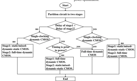
The timing and power optimization algorithm is shown in Fig. 6. We assume that either single clocking or multiple clocking dynamic CMOS is used in this flowchart. In order to operate in two stages, the circuit is partitioned to two stages. If the delays of two stages are equal, the design is in Case I; otherwise the design is in Case II. The circuit timing and power optimization analysis is based on the circuit Case classification:
1) Circuit in Case I
In single-clocking circuit, full-time dynamic CMOS is chosen for timing optimization.
In multiple-clocking circuit, stage1 and stage2 are implemented by static/mixed-dynamic-static CMOS and full-time dynamic CMOS, respectively, for power optimization meanwhile sustain operating speed.
2) Circuit in Case II
In single-clocking circuit, full-time dynamic CMOS is chosen for timing optimization; stage1 and stage2 are implemented by full-time dynamic CMOS and static/mixed-dynamic-static CMOS, respectively, for power optimization. In multiple-clocking circuit, stage1 and stage2 are implemented by static/mixed-dynamic-state CMOS and full-time dynamic CMOS, respectively, for power optimization.
Start
Partition circuit to two stages
Delay of stage1 = Delay of stage2?
Stage1: static/mixed-dynamic-static CMOS. Stage2: full-time dynamic CMOS. Full-time dynamic
CMOS
End
no yes
Single-clocking dynamic CMOS?
yes Single-clocking
dynamic CMOS? no
Stage1: static/mixed-dynamic-static CMOS. Stage2: full-time dynamic CMOS.
no
Timing is prior to power?
yes
Stage1: full-time dynamic CMOS. Stage2: static/mixed-dynamic-static CMOS.
no
[image:3.612.87.526.274.535.2]yes
Fig. 6 Timing and power optimization algorithm
IV. TIMING AND POWER OPTIMIZATION FOR CIRCUIT IN
CASE I
A 16-bit carry select adder (CSA) is used as a benchmark to demonstrate the proposed timing and power optimization in Case I. This section introduces a low-power 16-bit CSA, and timing and power optimization on it.
A. Low-Power 16-bit CSA
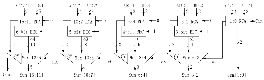
In general, the CSA is comprised of two main blocks: ripple carry adder (RCA) and multiplexer (Mux).
Two n-bit binary numbers are summed by two group of RCA‘s with carry-in of logic ‗0‘ and ‗1‘, respectively. The Mux select output of the RCA‘s with pre carry-in of logic ‗0‘ if the Cin = 0; otherwise, the RCA‘s with pre carry-in of logic ‗1‘ are selected [13].
International Journal of Emerging Technology and Advanced Engineering
Website: www.ijetae.com (ISSN 2250-2459, ISO 9001:2008 Certified Journal, Volume 6, Issue 11, November 2016)
22
15:11 RCA
6-bit BEC 0
1
5 5
A[15:11] B[15:11]
CY Mux 12:6
2 10
5 Sum[15:11]
10:7 RCA
5-bit BEC 0
1
4 4
A[10:7] B[10:7]
CY Mux 10:5
2 8
4 Sum[10:7]
6:4 RCA
4-bit BEC 0
1
3 3
A[6:4] B[6:4]
CY Mux 8:4
2 6
3 Sum[6:4] c6
3:2 RCA
3-bit BEC 0
1
2 2
A[3:2] B[3:2]
CY Mux 6:3
2 4
2 Sum[3:2] c3
1:0 RCA Cin
2 2
A[1:0] B[1:0]
2
Sum[1:0] c1
c10
o1 o2
o3 o4
[image:4.612.75.534.122.261.2]Cout
Fig. 7 Low-power 16-bit CSA
A modified low-power CSA is shown in Fig. 7. It replaces the RCA of carry-in ‗1‘ with compared low-power and area-efficient component, Binary to Excess-1 Converter (BEC) [14]. The BEC obtains the output of RCA with carry-in ‗0‘, and indicates the same output with RCA with carry-in ‗1‘. Area and power consumption of the low-power 16-bit CSA is reduced by 15% and 10.56%, respectively.
B. Timing and Power Optimization for low-power 16-bit CSA
In order to maintain the merit of high speed, all blocks in Fig. 7 are implemented by dynamic CMOS logic as reference for later performance comparison.
1) Low-power 16-bit CSA
According to the structure of full-time dynamic CMOS, the three stages in 16-bit CSA are partitioned to two groups, which will be evaluated in turn during evaluation
and pre-charge phase.
As seen in Fig. 7, RCA and BEC are parallel connected. Therefore, RCA- and BEC-stage are grouped to evaluate in one clock pulse. And Mux-stage is evaluated under another clock pulse. Because of the operating feature of full-time dynamic CMOS, the output of RCA/BEC-stage is discharged to ‗0‘. The CMOS transmission switches are inserted between RCA/BEC-stage and Mux-stage to hold the output values of RCA/BEC during pre-charge in Mux-stage.
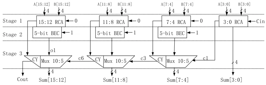
When the Mux-stage operates under the latter clock pulse, signal c1 and o1 arrive earlier than o4 in Fig. 7. It causes latency in signal propagation. In order to propagate signal efficiently, signal c1, o1, o2, o3 and o4 would rather arrive at the same time, thus next stage would start to evaluate in next clock pulse without latency. To solve this issue, we use all RCA‘s with the same size in Fig. 8.
According to the SPICE simulation, the timing of signal propagation from Cin to Sum15 (635ps) and that from B12 to o1 (660ps) in Fig. 8, are close. Then the circuit design belongs to Case I.
2) Timing and Power Optimization
The performance evaluation of delay, power, and maximum clock frequency for the low-power 16-bit CSA is presented in Table I, in which dynamic-dynamic-static (DDS) means the first and second stages in CSA are dynamic CMOS and the third one is static CMOS; static-static-dynamic (SSD) means the first and second stages in CSA are static CMOS and the third one is dynamic CMOS. Using multiple-clocking dynamic CMOS, several circuits operate in parallel and pipeline (shown in Fig. 3). The delay for data use is considered and the best platform for full-time dynamic SSD is multiple-clocking CMOS. The idea of designing SSD is to optimize clock pulse to reduce power and meanwhile satisfy the timing constraint. Half-time dynamic CMOS and full-Half-time DDS operate under single-clock. In Table I, timing of two critical paths,
and , are nearly same yet power consumption of is greater than that of
. Thus is the worst-case path for performance evaluation.
International Journal of Emerging Technology and Advanced Engineering
Website: www.ijetae.com (ISSN 2250-2459, ISO 9001:2008 Certified Journal, Volume 6, Issue 11, November 2016)
23
15:12 RCA
5-bit BEC 0
1
4 4
A[15:12] B[15:12]
CY Mux 10:5
4 Sum[15:12]
c6 c3
Cin
4
Sum[3:0] c1
Cout
11:8 RCA
5-bit BEC 0
1
4 4
A[11:8] B[11:8]
CY Mux 10:5
4 Sum[11:8]
7:4 RCA
5-bit BEC 0
1
4 4
A[7:4] B[7:4]
CY Mux 10:5
4 Sum[7:4]
3:0 RCA
4 4
A[3:0] B[3:0]
o1 Stage 1
Stage 2
[image:5.612.94.519.125.262.2]Stage 3
Fig. 8 Block diagram of 16-bit CSA with RCA in same size
TABLEI
PERFORMANCE OF MODIFIED 16-BIT CSA
Signal propagation Circuit type Delay (ps) Clock frequency (MHz) Power (mW)
Half-time dynamic CMOS 682 725 4.187
Full-time dynamic CMOS 235 909 9.878
Full-time dynamic CMOS (DDS) 233 794 8.934
Full-time dynamic CMOS (SSD) 285 379 2.082
Half-time dynamic CMOS 697 714 6.822
Full-time dynamic CMOS 234 862 9.866
Full-time dynamic CMOS (DDS) 233 758 9.017
Full-time dynamic CMOS (SSD) 288 463 2.55
Half-time dynamic CMOS 1,340 373 3.982
Full-time dynamic CMOS 789 633 7.889
Full-time dynamic CMOS (DDS) 835 602 7.557
Full-time dynamic CMOS (SSD) 784 413 2.333
Half-time dynamic CMOS 1,340 373 4.187
Full-time dynamic CMOS 789 633 8.216
Full-time dynamic CMOS (DDS) 831 602 7.988
Full-time dynamic CMOS (SSD) 788 413 2.388
Using multiple-clocking dynamic CMOS, power can be reduced by replacing the stage1&2 with static or mixed-dynamic-static CMOS that would not sacrifice timing.
[image:5.612.102.515.314.670.2]International Journal of Emerging Technology and Advanced Engineering
Website: www.ijetae.com (ISSN 2250-2459, ISO 9001:2008 Certified Journal, Volume 6, Issue 11, November 2016)
24
The power consumption of full-time SSD is about 70% and 43% less than that of full-time and half-time dynamic CMOS, respectively. Then full-time SSD is used for circuit power optimization.
V. TIMING AND POWER OPTIMIZATION FOR CIRCUIT IN
CASE II
A 64-bit binary comparator is used as a benchmark to demonstrate the proposed timing and power optimization in Case II. This section introduces a high-speed 64-bit binary comparator, and timing and power optimization on it.
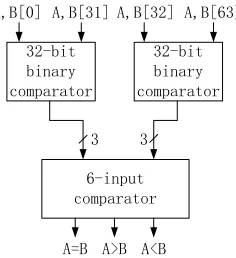
A. Module Design of the 64-bit Binary Comparator
Binary comparator is a basic digital arithmetic component that compares two binary numbers. A 64-bit binary comparator comprises two 64-bit binary input (
& - ) and three binary output, which indicates A>B, A<B, or A=B.
In recent years, researchers propose work on high performance 64-bit binary comparator design [15][16][17][18][19]. A competitive high-speed 64-bit binary comparator is introduced and used to demonstrate our approach to timing and power optimization in Case II. The delay and power of the 64-bit comparator are 738.5ps and 13.21mW respectively, which is implemented in 250nm CMOS process.
The module design of the 64-bit binary comparator is shown in Fig. 9, in which the higher order 32-bit binary comparator‘s outputs, ―A>B‖ or ―A<B‖, dominate the 6-input binary comparator‘s outputs, ―A>B‖ or ―A<B‖. If the higher order 32-bit binary comparator result is ―A=B‖ then the lower order 32-bit binary comparator‘s output dominate the 6-input comparator‘s output.
32-bit binary comparator
32-bit binary comparator
6-input comparator
3 3
A=B A>B A<B
[image:6.612.335.553.199.320.2]A,B[0] A,B[31] A,B[32] A,B[63]
Fig. 9 Block diagram of 64-bit binary comparator
In Fig. 10, the 8-bit binary comparator is applied to compare two 8-bit binary numbers and the output (A>B, A=B, or A<B) is fed to a 12-input binary comparator. As the operation of 6-input comparator, the four 8-bit binary comparator dominate the 12-input comparator in turn by order.
8-bit binary comparator
8-bit binary comparator
8-bit binary comparator
8-bit binary comparator
12-input comparator A,B[0]
3 3 3 3
A=B A>B A<B
[image:6.612.110.228.509.638.2]A,B[7] A,B[8] A,B[15] A,B[16] A,B[23] A,B[24] A,B[31]
Fig. 10 Block diagram of 32-bit binary comparator
B. Design of Blocks in 64-bit Binary Comparator
This section introduces design of 6/12-input comparator in detail. Other blocks‘ design and simulation result are analyzed in [20].
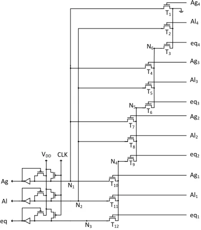
1) 12-input Comparator
The 12-input comparator is used to compare the outputs of four binary comparators in order. The equations of three outputs of 12-input comparator is simplified down to (1), in which eq, Ag, Al indicate binary input A=B, A>B, A<B, respectively.
{
eq
International Journal of Emerging Technology and Advanced Engineering
Website: www.ijetae.com (ISSN 2250-2459, ISO 9001:2008 Certified Journal, Volume 6, Issue 11, November 2016)
25
Ag4
Al4
eq4
Ag3
Al3
eq3
Ag2
Al2
eq2
Ag1
Al1
eq1 VDD CLK
Ag
Al
eq
N1
N2
N3 N4
N5 N6
T1
T2
T3
T4
T5
T6
T7
T8
T9
T10
T11
[image:7.612.326.559.110.414.2]T12
Fig. 11 Structure of dynamic 12-input comparator
To acquire maximum operating speed, the transistor size in Fig. 11 is optimized according to the algorithm in [4]. The optimized transistor size is (360nm), (360nm), (3180nm), (360nm), (360nm), (1920nm), (540nm), (540nm), (540nm), (540nm), (540nm), (360nm) of 250nm process.
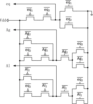
Fig. 12 presents transistor level structure of static 12-input comparator according to (1).
Vdd
eq1
eq
Ag
eq2 eq3 eq4
eq1
eq2
eq3
eq4
Ag4
eq4 Ag3
eq3 Ag2
eq2 Ag1
Ag4 eq4
Ag3 eq3
Ag2 eq2
Ag1
Al
Al4
eq4 Al3
eq3 Al2
eq2 Al1
Al4 eq4
Al3 eq3
Al2 eq2
Al1
Fig. 12 Structure of static 12-input comparator
2) 6-input Comparator
[image:7.612.58.259.123.353.2]International Journal of Emerging Technology and Advanced Engineering
Website: www.ijetae.com (ISSN 2250-2459, ISO 9001:2008 Certified Journal, Volume 6, Issue 11, November 2016)
26 { eq
Then based on (2) the transistor level schematic of 6-input comparator in dynamic CMOS is designed in Fig. 13.
Ag2 Al2 eq2 Ag1 Al1 eq1
VDD CLK
[image:8.612.327.561.212.432.2]Ag Al eq N1 N2 N3 N4 T1 T2 T3 T4 T5 T6
Fig. 13 Structure of dynamic 6-input comparator
With optimizing transistor size according to the algorithm in [4], transistor size in Fig. 13 is (1380nm),
(840nm), (660nm), (360nm), (1200nm), (540nm) of 250nm process.
The transistor level structure of static 6-input comparator is sketched in Fig. 14 according to (2).
Vdd eq1 eq Ag eq2 eq1 eq2 Ag2
eq2 Ag1 Ag2
eq2
Ag1
Al
Al2
eq2 Al2 Al2
eq2
[image:8.612.58.278.215.371.2]Al2
Fig. 14 Structure of static 6-input comparator
C. Timing and Power optimization for 64-bit binary comparator
As shown in Fig. 15, a 64-bit binary comparator consists of four operation-stages: 2-bit binary comparator, 12-input comparator, and 6-input comparator. Partition of 64-bit binary comparator and its timing and power optimization are discussed in this section.
2-bit binary comparator 2-bit binary comparator 2-bit binary comparator 2-bit binary comparator 12-input comparator A,B62 A,B63 3 3 3 3 6-input comparator A=B A>B A<B A,B60 A,B61 A,B58 A,B59 A,B56 A,B57 2-bit binary comparator 12-input comparator A,B48 A,B55 12 . . . 2-bit binary comparator 12-input comparator A,B40 A,B47 12 . . . 2-bit binary comparator 12-input comparator A,B32 A,B39 12 . . . 2-bit binary comparator 12-input comparator A,B0 A,B31 48 . . . 12-input comparator 3 3 3 3 12-input comparator 12 3 3
Stage 1 Stage 2 Stage 3 Stage 4
Fig. 15 Block diagram of 64-bit binary comparator
1) Partition of 64-bit binary comparator
As mentioned in section II, the fastest conventional design for 64-bit binary comparator is full-time dynamic CMOS that requires to separate the four stages of 64-b comparator to two groups, which will be evaluated in evaluation and pre-charge, respectively.
According to the simulation of half-time (conventional) dynamic 64-bit binary comparator, the timing of signal propagation through stage1&2 (417ps) and that through stage3&4 (321ps) are close, so the best choice is that group stage1&2 together to operate under one clock pulse and group stage3&4 together to operate in next clock pulse. Absolutely, CMOS switch should be inserted between two groups in order to hold the output of first group for second one during the evaluation-phase of second group.
2) Timing and Power optimization
[image:8.612.90.247.474.649.2]International Journal of Emerging Technology and Advanced Engineering
Website: www.ijetae.com (ISSN 2250-2459, ISO 9001:2008 Certified Journal, Volume 6, Issue 11, November 2016)
27
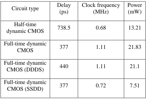
The analysis of delay, power consumption, and maximum clock frequency of dynamic, static, and mixed-dynamic-static 64-bit binary comparator is shown in Table II, in which DDDS means the first, second, and third stages in Fig. 14 are dynamic CMOS and the forth one in it is static CMOS; SSDD means the first and second stages are static CMOS, the third and fourth one in it are dynamic CMOS. In multiple-clocking dynamic CMOS, the delay for data use plays more important role than its clock frequency. Then the best platform for full-time dynamic SSDD 64-bit binary comparator is multiple-clocking CMOS, because it can sacrifice clock pulse, which is not important, to achieve low power; other full-time dynamic CMOS and half-time dynamic CMOS should operate in single-clocking CMOS, because they can keep the highest clock frequency. In Table II, ―Delay‖ is the worst delay of 64-bit binary comparator, signal propagation from input ―A0‖ to output ―A=B‖; ―Clock frequency‖ is the maximum clock frequency under that the circuit can operate functionally; ―Power‖ is the average power consumption of operation under worst case.
TABLEII
POWER AND TIMING OF 64-BIT BINARY COMPARATOR
Circuit type Delay (ps)
Clock frequency (MHz)
Power (mW)
Half-time
dynamic CMOS 738.5 0.68 13.21
Full-time dynamic
CMOS 377 1.11 21.83
Full-time dynamic
CMOS (DDDS) 440 1.11 21.1
Full-time dynamic
CMOS (SSDD) 377 0.72 7.51
In single-clocking dynamic CMOS, in order to keep operating speed, the clock frequency cannot be sacrificed. However, the first stage-group takes more timing than the second one, so the second stage-group can be implemented by mixed-dynamic-static CMOS to decrease power consumption and still maintain clock frequency. The timing of stage3 (206ps) occupies roughly 64% of that of the second stage-group (321ps), but the delay of stage-group 1 (417ps) is just 29.9% greater than that of stage-group 2 (321ps), then only stage4, which is smaller than stage3, can be replaced by static CMOS in order to maintain clock speed.
So in single-clocking dynamic CMOS, if power is prior to timing, full-time dynamic DDDS CMOS should be chosen; otherwise full-time dynamic CMOS is the optimal choice. As seen in Table II, the delay of full-time dynamic CMOS (377ps) is almost half of that of half-time dynamic CMOS (738.5ps), and 14.3% less than that of full-time dynamic DDDS CMOS; full-time dynamic DDDS CMOS and full-time dynamic CMOS have the same clock frequency, but the power consumption of the DDDS (21.1mW) is decreased by 3.3% compared with full-time dynamic (21.83mW). Then for single-clocking circuit, full-time dynamic CMOS is chosen for timing optimization; stage1 and stage2 are implemented by full-time dynamic CMOS and static/mixed-dynamic-static CMOS, respectively, for power optimization.
In multiple-clocking dynamic CMOS, the delay for data use plays more important role than its clock pulse, then clock frequency can be sacrificed to decrease power consumption that can be implemented by replacing stage-group 1 in Fig. 15 with static CMOS. Then highest clock frequency of full-time dynamic SSDD (0.72MHz) is 54.2% less than that of other full-time dynamic COMS, the best choice for multiple-clocking CMOS is still SSDD. As shown in Table II, the delay of full-time dynamic SSDD CMOS (377ps) is the same with that of full-time dynamic CMOS, and 14.3% and 50% less than that of full-time dynamic DDDS CMOS (440ps) and full-time dynamic CMOS (738.5ps), respectively; the power consumption of full-time dynamic SSDD CMOS is about 43.1%, 65.6%, and 64.4% less than that of full-time dynamic CMOS, half-time dynamic CMOS, and full-half-time dynamic DDDS, respectively. Then for multiple-clocking circuit, stage1 and stage2 are implemented by static/mixed-dynamic-static CMOS and full-time dynamic CMOS, respectively, for power optimization.
VI. CONCLUSION
A general technique of power and timing optimization for dynamic CMOS has been proposed in this paper. 16-bit CSA and 64-bit binary comparator are applied as benchmarks.
[image:9.612.41.295.384.556.2]International Journal of Emerging Technology and Advanced Engineering
Website: www.ijetae.com (ISSN 2250-2459, ISO 9001:2008 Certified Journal, Volume 6, Issue 11, November 2016)
28
For 64-bit binary comparator, if it is applied in single-clocking circuit, timing optimization should choose full-time dynamic CMOS, whose delay is decreased by 49% compared with the conventional (half-time) dynamic CMOS, and in power optimization, the CMOS evaluated in later clock pulse should be implemented by mixed-dynamic-static CMOS, in which the circuit power consumption is decreased by 3.3% meanwhile maintain speed. If it is applied in multiple-clocking circuit, the CMOS evaluated in former clock pulse should be designed by static CMOS. In comparison with the conventional (half-time) dynamic CMOS, the power consumption and delay are reduced by 43.1% and 49%, respectively.
REFERENCES
[1] L. Zhang, ―Statistical Timing Analysis for Digital Circuit Design,‖ Ph.D dissertation, University of Wisconsin-Madison, Madison, WI, 2005.
[2] S. Ziabakhsh, ―An ultra-high speed low-power CMOS integrated current comparator,‖ in IDT, 2008, pp. 159-164.
[3] V. Thrivikramaru, ―High Speed Low Power CMOS Current Comparator,‖ in CSNT, 2012, pp. 764-768.
[4] K. Yelamarthi and H. Chen, ―Process Variation-Aware Timing Optimization for Dynamic and Mixed-Static-Dynamic CMOS Logic,‖ IEEE Transactions on Semiconductor Manufacturing, vol. 22, no. 1, Feb. 2009.
[5] N.H.E. Weste and D.M. Harris, ―CMOS VLSI Design,‖ 4th ed., pp. 339-341.
[6] Z. Liu and V. Kursun, ―Shifted leakage power characteristics of dynamic circuits due to gate oxide tunneling,‖ in SOC, 2005, pp. 151–154.
[7] Z. Liu and V. Kursun, ―Leakage biased PMOS sleep switch dynamic circuits,‖ IEEE Trans. On Circuits Syst., vol. 53, no. 10, Oct. 2006. [8] S.B. Wijeratne, N. Siddaiah, S.K. Mathew, M.A. Anders, R.K.
Krishnamurthy, J. Anderson, M. Ernest, and M. Nardin, ―A 9-GHZ 65-nm Intel Pentium 4 processor integer execution unit,‖ IEEE J. Solid-State Circuits, vol. 42, no. 1, Jan. 2007.
[9] N.F. Goncalves and H.J.D. Man, ―NORA: A racefree dynamic CMOS technique for pipelined logic structures,‖ IEEE J. Solid-State Circuits, vol. SC-18, no. 3, pp. 261–266, Jun. 1983.
[10] V. Kursun and E.G. Friedman, ―Variable threshold voltage keeper for contention reduction in dynamic circuits,‖ in ASIC/SOC, 2002, pp. 314–318.
[11] V. Kursun and E.G. Friedman, ―Domino logic with dynamic body biased keeper,‖ in ESC, 2002, pp. 675–678.
[12] S. Mathew, M. Anders, R.K. Krishnamurthy, and S. Borkar, ―A 4-GHz 130-nm address generation unit with 32-bit sparse-tree adder core,‖ IEEE J. Solid-State Circuits, vol. 38, no. 5, pp. 689–695, May 2003.
[13] Y. Kim, ―A low power carry select adder with reduced area,‖ in ISCAS, 2001.
[14] B. Ramkumar and H.M. Kittur, ―Low-Power and Area-Efficient Carry Select Adder,‖ IEEE Trans. On VLSI Systems, vol. 20, no. 2, pp. 371-375, Feb. 2012.
[15] C.-H. Huang and J.-S. Wang, ―High-performance and power-efficient CMOS comparators,‖ IEEE J. Solid-State Circuits, vol. 38, no. 2, pp. 254-262, Feb. 2003.
[16] H.-M. Lam and C.-Y.Tsui, ―A MUX-based high-performance single-cycle CMOS comparator,‖ IEEE Trans. Circuits Syst. II, Exp. Briefs, vol. 54, no. 7, pp. 591-595, Jul. 2007.
[17] J.-Y. Kim and H.-J.Yoo, ―Bitwise competition logic for compact digital comparator,‖ in ASSCC, 2007, pp. 59-62.
[18] S. Perri and P. Corsonello, ―Fast low-cost implementation of single-clock-cycle binary comparator,‖ IEEE Trans. Circuits Syst. II, Exp. Briefs, vol. 55, no.12, pp. 1239-1243, Dec. 2008.
[19] F. Frustaci, S. Perri, M. Lanuzza, and P. Corsonello, ―A new low-power high-speed single-clock-clock-cycle binary comparator,‖ in ISCS, 2010, pp. 317-320.