International Journal of Emerging Technology and Advanced Engineering
Website: www.ijetae.com (ISSN 2250-2459, ISO 9001:2008 Certified Journal, Volume 9, Issue 5, May 2019)
198
Modeling and Simulation of a Terminated Type MEMS Power
Sensor Using Hybrid FE/FDTD Technique
Edriss Ahmed Ali
1, Muamba Kabula
2, Hans L. Hartnagel
21Al-Ghurair University, College of Engineering and Computin, P. O. Box 37374, Dubai, UAE 2Institut fuer Hochfrequenztechnik, Technische Universitaet Damstadt D-64283 DARMSTADT, Germany
Abstract— A theoretical simulation model for characterization of the electrical and thermal behavior of MEMS power sensors at both the dc and high frequencies (microwave and millimeter waves) is presented, in this paper. The simulation is based on the solution of the coupled electromagnetic field and heat transfer equations, using hybrid finite-element/finite-difference-time-Domain (FE/FDTD) techniques. The sensor fabrication technique is based on bulk and surface micromachining of AlGaAs/gaAs heterostructures. The model can be used as an effective tool for adjustment of design parameters, such as geometric configuration of the sensor resistive element, and arrangement of thermocouples around the resistor for optimum sensitivity and noise figure. Simulated results were verified with experimental measurements with good agreement.
Keywords— simulation; modeling; finite element; FDTD; MEMS; power sensors
I. INTRODUCTION
Detection and continuous monitoring of the RF power delivered from microwave monolithic integrated circuits (MMIC) directly on the chip is desirable and plays an important role in many applications of the modern communication systems. Information obtained from such measurements could be used for many purposes such as evaluation of reflection coefficients, monitoring of microwave power level in integrated microwave circuits, gain control in amplifiers, or possible failure detection of transmitter subsystems. Many MEMS sensor configurations have recently been introduced [1–6]. The sensor concept is based on transduction principle that converts the RF power into thermal power, which is then measured by thermoelectric means. These sensors were based on coplanar waveguide (CPW) technology, thus offering compatibility to the standard MMIC technology, and were realized either on silicon [1,2] or GaAs [3-6]. GaAs based sensors were realized by either of two configurations. The first used the Joule heating losses of the center conductor of the CPW, which is an intrinsic effect of the CPW [3,4].
The other configuration employed a terminating resister, matched to the characteristic impedance of a 50 Ohm CPW [5,6], in which RF power is dissipated and converted into heat. Recently power sensors, based on capacitive MEMS technology, in which a small portion of transmitted power for measurement, is detected have been introduced [9,10]. Even in this later type, the final stage of power determination is based on the principles of electro-thermal conversion in a terminating resistor.
The sensor considered here is of the terminating resistor type, but instead of using a coplanar waveguide as a feeding transmission line, a coplanar strip line (CPS), is used as a matching section to a dipole antenna [7]. Coplanar strip line is used for its many advantages, compared to CPW in such applications, among which, the finite size of its ground, efficient use of wafer area and sustainable back metallization without exciting parasitic modes within the range of operating frequencies [8].
Proper design of MMIC sensors, and MMIC devices in general, requires reliable modeling tools before actual fabrication. This is necessary in order to have precise priori knowledge of the device performance, and hence avoid time consuming and costly redesign cycles. Modeling and simulation have special importance in the micro-world of MEMS, in which many physical phenomena take place. GaAs-based sensors have been electrically characterized and the obtained higher sensitivities and broadband response are promising for the monolithic integration of power-sensing functions in future RF devices [5]. Electro-thermal models for simulation of heat transfer and temperature distribution were developed and used by a number of authors for both silicon and GaAs-based sensors [9,10]. However these models were based on simple equivalent circuit elements and solved using SPICE [10].
International Journal of Emerging Technology and Advanced Engineering
Website: www.ijetae.com (ISSN 2250-2459, ISO 9001:2008 Certified Journal, Volume 9, Issue 5, May 2019)
199
II. DESCRIPTION OF THE PHYSICAL PROBLEM
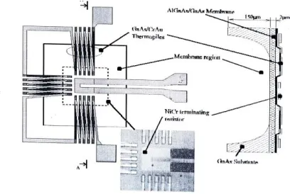
A sectional view of the first configuration of the sensor to be modeled is depicted in Figure 1. The sensor is composed of a thermally isolated thin (2 μm) AsGaAs/GaAs membrane region with a terminating resistor, in which heat generated by RF power is dissipated and converted into heat. A high-thermally resistive membrane region is obtained by selective etching of the GaAs against AlGaAs. This helps to increase temperature gradient between the resistor region and the rest of the chip, thus leading to high sensitivity. Temperature increase in the resistor region is sensed by a set of Gs/Au-Cr thermo-elements, whose dc output is proportional to the input RF power.
[image:2.612.327.557.275.394.2]Unlike most of the reported sensors which are fed by 50 Ohm coplanar waveguides [3,4], the requirement here is to match the terminating resistor to a dipole antenna that detects RF power [7]. Therefore a matching network is realized by a coplanar strip-line that connects the antenna with the heating resistor on the membrane. With the later, a simplification of the fabrication process is achieved. However, for separate characterization of the sensor, the antenna is disconnected and an additional line segments are introduced to form SGS electrode configuration for on-wafer measurements. Detailed description of technical realization of this sensor is given in [7].
Figure 1. The structure of the power sensor. left-hand : top view, right-hand-side sectional view along A-A’.
III. THE MATHEMATICAL MODEL
Here we consider both the thermal and the electric models. The mathematical model is required to be simple enough to be handled by known methods which demand reasonable time and cost, and at the same time give an adequate description of the physical problem under investigation.
A. Thermal Model
A simplified pictorial view of the sensor is shown in Figure 2 for the purpose of thermal modeling. Here the thermocouple wires are not shown, and heat generated by the NiCr resistor, is assumed to be distributed throughout the sensor structure mainly by conduction. Due to axial symmetry of the sensor structure about it longitudinal axis, we only consider half of its geometry as shown in Figure 3. We select Cartesian coordinates (x,y,z) with its origin at the sensor input and the direction of power transmission along the positive z-direction.
Figure 2. Simplified half-section used for modeling.
In order to obtain a simple and manageable model, the following simplifying assumptions, are made:
1. The presence of the thermocouples is ignored as the metallic part (gold) is very small compared to other dimensions.
2. As a first approximation, heat distribution is assumed to be two-dimensional (in Y-Z plane). This assumption can be justified due to the presence of the thermally isolated thin membrane whose area dominates the horizontal dimensions of the sensor. 3. Constant thermal properties. Although thermal
properties, especially thermal conductivity of GaAs vary with temperature [11], these properties were assumed to be constant due to the expected moderate temperature rise.
4. Radiation losses are ignored as the sensor was to work in a very confined region and the expected temperature rise is limited.
The equation governing heat flow as a result of microwave or dc heating is the well-known heat conduction equation, also known as Fourier equation:
C
Q
T
t
T
/
2
[image:2.612.69.273.445.582.2]International Journal of Emerging Technology and Advanced Engineering
Website: www.ijetae.com (ISSN 2250-2459, ISO 9001:2008 Certified Journal, Volume 9, Issue 5, May 2019)
200
Where T is the temperature, α is thermal diffusivity , Q heat generation term, ρ is the density and C is the specific heat of the medium .
Thermal Boundary Conditions: In order to find unique solutions of the heat equation appropriate boundary and initial conditions have to be made. These conditions can be obtained from the prevailing thermal conditions at the boundaries and the interface between different material layers of the sensor.
i) Convective heat transfer at Boundaries:
By assuming that the temperature outside the sensor (Y > a) is at a constant value T(a), then from Newton’s law of cooling: )) a ( T -) t , z , a , x ( T ( h = ) t , z , a , x ( y T K (2.a)
where K is thermal conductivity and h is the convective heat transfer coefficient assumed to be constant.
ii) Specified temperature at Boundaries:
Here we assume that the sensor is at a constant temperature T1 at z= 0 and z = L, giving:
1 1
)
,
,
,
(
)
,
0
,
,
(
T
t
L
y
x
T
T
t
y
x
T
(2.b)iii) At the interface between different sensor material layers:
Assuming perfect thermal contact leads to the continuity of heat flux and temperature at these interfaces:
j
&
i
layers
between
j i j iT
T
i
t
T
K
i
y
T
K
(2.c)Assume initially that the sensor is at a constant temperature, T0 i.e.
T
(
x
,
y
,
z
,
0
)
T
0 (2.d)The heat source term, Q, in equation (1), is determined by solving either of two different sets of equations, depending on the operation mode of the sensor (dc or high frequency).
B. Electromagnetic Model
Here we consider the case of AC and DC case separately, because of their different governing equations.
DC Operation Mode: In the case of the dc operation mode, the electrostatic potential equation is used:
(
V
)
q
i (3)where V is the electrical potential, σ is the electrical conductivity, and qi is the current source. In the case of
constant electrical conductivity, equation (3) reduces to the simple Poisson’s equation:
/
2 iq
V
(4)Boundary conditions assumed for solution of equation (4) were that a constant voltage +V applied at one arm and –V at the other arm of the CPS With the symmetry condition along the longitudinal axis of the sensor, +V was assumed at one arm at input of the sensor and zero voltage at the end of the resistor (see Figure (1b)). Having found V from equation (4), the heat generation term, Q, is obtained as:
Q
E
2 (5)where E is the electric field intensity, given by:
V
E
(6)
High Frequency Mode: In the case of high frequency operation mode, the heat generation term, Q, is obtained from the solution of Vector Maxwell’s equations:
t
X
E
H
(7)
t
X
H
E
E
(8)
in which
E
and
H
are electric and the magnetic field vectors, and , , are respectively the permittivity, the permeability and the conductivity of the material (medium) through which electromagnetic wave propagation takes place.C. Solution of the Governing Equations
International Journal of Emerging Technology and Advanced Engineering
Website: www.ijetae.com (ISSN 2250-2459, ISO 9001:2008 Certified Journal, Volume 9, Issue 5, May 2019)
201
The method adopted however, depends on the sensor structure and the type of the boundary condition to be assumed at the sensor boundaries. If the simplifying assumption (i) – (iv) are used, equation (1) with boundary conditions ii), iii) and iv) can be solved analytically using the method of separation of variables. However, in the more general case of three-dimensional form of equation (1) with boundary conditions (i) to (iv), the versatile numerical methods of finite difference in time-domain or finite elements are more appropriate, since they can deal with any sensor structure.
Investigation of available software packages revealed that XFDTD package, based on finite difference time domain technique, is most appropriate for the solution of ector Maxwell's equations.
The output of this package was then used as input for the heat equation, which was solved using FEMLAB, a package, based on finite-element technique. As the two packages (FEMLAB and XFDTD) are based on different solution techniques using different meshing schemes, it was necessary to have an interface that for linking the two packages. This was achieved by a special script file written using MATLAB built-in functions. Material properties used in the simulation ate shown in Table 1.
TABLE 1
ELECTRICAL AND THERMAL PROPERTIES USED IN THE SIMULATION
Material
Thermal conductivity (W/m K)
Specific heat (J/kg K)
Density (kg/m3)
Relative permittivity
Electrical conductivity (mho)
GaAs 44 334 5360 12.8 5x10⁻⁴
NiCr 22 450 8300 - 9.1x10⁵
Au 315 130 1928 - 4.5x10⁷
Al/GaAs 23.7 445 3968 - 5x10⁻⁴
IV. EXPERIMENTAL SET-UP AND MEASUREMENTS
Due to the small dimensions of the sensor structure, it was difficult to determine temperature distribution by direct temperature measurements. Therefore, a technique based on thermal imaging was used [11]. The top surface of the test structures were coated with a thin film of liquid crystal (R35CW 0.7 from Hallcrest Inc, UK), that changes color with the changes in the sensor surface temperature.
This change in temperature was monitored by a CCD camera connected to a microscope and a personal computer was used to store the recorded shots for later analysis. For dc operation mode, a stable current source was used, and both the input voltage and current were monitored for accurate determination of input power (see Figure 3).
For RF mode of operation, the current source was replaced by an RF probe that connected directly to the input pads of the CPS.
Figure 3. Block diagram of the experimental set-up for sensor test
V. RESULTS AND DISCUSSIONS
D. Simulation Results
[image:4.612.323.580.245.414.2]International Journal of Emerging Technology and Advanced Engineering
Website: www.ijetae.com (ISSN 2250-2459, ISO 9001:2008 Certified Journal, Volume 9, Issue 5, May 2019)
202
Figure 5. Enlarged view of temperature distribution around thecorner of the resistive termination
[image:5.612.63.284.150.460.2]Figure 6 shows temperature profile on a line passing through the hottest point (across y-direction) of the resistor due to an input voltage of 0.8V. This high gradient of temperature across the resistor illustrates the need for the thermocouples to be as near as possible to the resistor edge to have high sensitivity, as expected. Figure 7 shows temperature variation along the resistor (x-direction) and it clearly illustrates the effect of the gold strip on temperature distribution. Here the gold strip acts as an easy path for temperature due to its high thermal conductivity and this could also lead to degradation of sensitivity. Similar observations were reported by Milonovic et al. [9], when considering coplanar CMOS sensors based on coplanar waveguides (CPW), in which case, the ground plane had a degrading effect on sensitivity.
Figure 6 Temperature distribution across the resistive termination (y-direction) of Figure 2 (input 0.8 v)
Figure 7 Temperature variation along the sensor (x-direction).
Figure 8 shows temperature distribution around the long arm of the resistor together with the positions of the thermocouple tips at a constant distance of 20 μm from the outer edge of the resistor. Here Thi (i=1,2,..), represents
thermocouple i, with i=1 at the junction between the gold strip and the resistor. It is clearly shown that different thermocouples indicate different temperature levels, with the center thermocouple (i=3) at the highest temperature level and the first (i=1) at the lowest temperature level. The difference between the maximum and the minimum levels is around 20 0K, for this particular setup, equivalent to a difference of about 50%. This has implication on the positioning of the thermocouple tips (hot junctions) around the resistor. The most important implication is that, thermocouple tips positioned at equal distances from the resistor, as was the case of earlier design of power sensors (see Figure 1), will not give the same level of temperature. These results give some guidelines on the positioning of thermocouple tips in the future improved designs of power sensors.
[image:5.612.345.544.294.441.2]International Journal of Emerging Technology and Advanced Engineering
Website: www.ijetae.com (ISSN 2250-2459, ISO 9001:2008 Certified Journal, Volume 9, Issue 5, May 2019)
203
Figure 8 Maximum temperature levels at the tips of thethermocouples along the x-direction
[image:6.612.330.562.381.586.2]Figure 9.a. shows a pictorial 3D color plot of temperature distribution on the top surface of the sensor, as predicted by simulation, and Figure 9.b shows accumulation of current density around the inner corner of the resistor is. This latter figure shows the possibility of destruction of the resistor at one of its sharp inner corners due to high concentration of the current at these corners.
[image:6.612.75.279.389.507.2]Figure 9.a. Pictorial color plot of temperature distribution on the top surface of the sensor
Figure 9.b Current density (J) at the inner corner of the resistive element
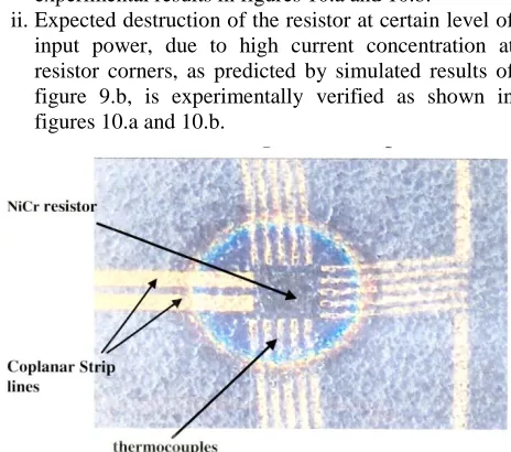
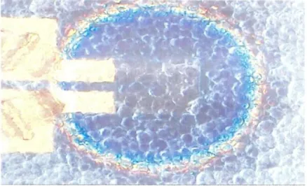
E. Experimental Results
Figures 10.a,b show the experimental results; one with thermocouples in place on the sensor (Figure 10.a) and the other without thermocouples (Figure 10.b). The experimental results were obtained by increasing the input power level at small increments until the resistor was destroyed at an input power level of about 80 mW. These experimental results show that the degree of destruction is more severe (as illustrated by the size of the elliptical shape surrounding the resister) when the thermocouples are removed (Figure 10.b). This can be attributed to spreading of heat away from the resistive termination by thermocouples when they present, thus decreasing level of destruction.
Comparison of figures 9 and 10 shows how the simulated results resemble the experimentally obtained results, at least qualitatively, in that:
i. Temperature distribution around the resistive element has the same elliptical shape of in both the theoretically simulated results (figure 9.a) and the experimental results in figures 10.a and 10.b.
ii.Expected destruction of the resistor at certain level of input power, due to high current concentration at resistor corners, as predicted by simulated results of figure 9.b, is experimentally verified as shown in figures 10.a and 10.b.
[image:6.612.56.285.552.668.2]International Journal of Emerging Technology and Advanced Engineering
Website: www.ijetae.com (ISSN 2250-2459, ISO 9001:2008 Certified Journal, Volume 9, Issue 5, May 2019)
[image:7.612.57.276.144.277.2]204
Figure 10.b Measured temperature distribution on the top surface ofthe sensor structure without thermocouples
VI. CONCLUSIONS
A theoretical thermal simulation model and fabrication of micromachined microwave power sensors, has been developed. The fabrication technique was based on bulk and surface michromachining of AsGaAs/GaAs heterostructures. The simulation model was based on the solution of the coupled electromagnetic and heat equations, using hybrid finite element/ finite difference techniques. The model was implemented on the computer using two simulation packages: FEMLAB, finite-element simulation package, and XFDTD, a finite-difference simulation package. On the practical experimental side, a number of experimental measurements were made on micromachined test sensor structure. These measurements were mainly concerned with determination of temperature distribution on test structures, using the method of liquid crystal imaging. Experimental results obtained were compared with theoretical findings with good agreement. Moreover, the simulation model showed that some resistive elements without sharp corners e. g. circular instead of semi-rectangular form modification could be made for optimized sensor design. These modifications include:
i) Geometric configuration of the sensor resistive elements.
The resistive element in the present design of the sensor takes a semi-rectangular shape with sharp (900) corners. These sharp corners help in accumulation of electric field and the creation of hot spots at these regions, thus leading to sensor failure or destruction, when power is increased. The suggested modification in future sensor designs could be making.
ii) Arrangement of thermo-sensors around the resistive element.
Both theoretical and experimental results showed that thermocouples placed side-by-side at equal distances from the resistive element do not sense the same level of temperature. This is due to the fact that the temperature distribution on the sensor surface takes a semi- elliptic shape around the resistor. This calls for rearrangements of these thermocouples so as to maximum overall sensor sensitivity.
Acknowledgments
We would like to express our gratitude to the German Academic Exchange Service (DAAD) for supporting this work, and the Institute of High Frequency, Technical University of Darmstadt, Germany, where the work was carried out.
REFERENCES
[1] Jaeggi, A.; Baltes, H.; and Moser D. Thermoelectric AC Power Sensor by CMOS Technology. IEEE Electric Dev. Lett. 1992, 13(7). 366-368.
[2] Kopystynski, P.; Obermayer, H.; Delfs, H.; Hohenester, W. and Loser, 1990. A. Silicon RF Power Sensor from D.C. to Microwave. In Microsystems Technologies 90, Springer, Berlin, pp. 605-610. [3] Dehe, A.; Krozer, V.; Fricke, K. Klingbeil, H.; Beilenhoff K. and
Hartnagel, H.L. 1995. Integrated Microwave Power Sensor. Electronics Letters; Vol. 31, No. 25, pp. 2187-2188.
[4] Dehe, K.; Klingbeil, H.; Krozer, V.; Fricke, K.; Beilenhoff, K. and Hartnagel, H.L. 1996. GaAs Monolithic Integrated Microwave Power Sensor in Coplanar Waveguide Technology. IEE Microwave and Millimeter-Wave Monolithic Circuits Symp.
[5] Dehe, a.; Krozer, V.; Chen, B. and Hartnagel, H.L. 1996. High-sensitivity microwave power sensor for GaAs-MMIC implementation. Electronic Lett. Vol. 32, No. 23, pp. 2149-2150. [6] Hartnagel, H. L.; Megej, A.; and Mutamba, K. 2001. Microwave and
millimeter-wave monolithic signal source with MEMS-based power monitoring for sensing applications. Abstract Book ONR Workshop on Physical Effects and Device/Circuit Interactions in Solid State Devices, Bar Harbor, USA.
[7] Mutamba, K.; Beilenhoff, K.; Megej, A.; Doerner, R.; Genc, E.; Fleckenstein, A.; Heymann, P.; Dickmann, J.; Woelk, C. and Hartnagel H.L. 2001. Micromachined 60 GHz GaAs power sensor with integrated receiving antenna, IEEE MTT-S Digest, pp.2235-2238.
[8] Kavita Goverdhanam; Rainee N.Simons; Nihad Dib and Linda Katehi. 1997. Coplanar Stripline Components for High Frequency Applications, IEEE Trans., MTT Vol. 45, pp: 1725 – 1729. [9] Veliko Milanovic; Molt Hopcroft; Christian A.; Zincke, Micheal
International Journal of Emerging Technology and Advanced Engineering
Website: www.ijetae.com (ISSN 2250-2459, ISO 9001:2008 Certified Journal, Volume 9, Issue 5, May 2019)
205
[10] Yinglin and Lino Xioaping. 2009. Design and fabrication of a terminating type MEMS microwave power sensor. Jr. Semiconductors. Vol. 30, No. 4. April 2009.