© 2017, IRJET | Impact Factor value: 5.181 | ISO 9001:2008 Certified Journal | Page 105
A Design Implementation of Single Stage Amplifiers using HEMT
Technology
Poornima Baliga M
1, Dr. Vasundara Patel K S
2,
1
Dept. Of Electronics & Communication Engineering, B.M.S. College of Engineering, Bangalore-560019
2Assistant Professor, Dept. of ECE, B.M.S. College of Engineering, Banglore-560019
---***---Abstract -
The capacity of Si-CMOS scaling down to deliverimproved performance has recently come into interrogation. The transfer properties of definite III-V compound semiconductors make HEMT to work smart for high frequency. HEMTs operation has been verified using several materials, especially AlGaAs/GaAs and AlGaN/GaN. This paper provides a CS amplifier and a source follower design tuned to 100GHz with three different substrate materials.
Key Words:CMOS; HEMT, CS Amplifier, source follower,
GaAs, GaN, Gain.
1.INTRODUCTION
Semiconductor industry is based on the silicon material from the time of its innovation. It is the material chosen when compared to germanium because of its advantages of being easily available in nature and less expensive. Silicon dioxide grown is a very good insulator which shrinks processing complexity. This oxide is also soluble in water. These features supports in fabricating MOSFETs [1]. The revolution which took place in microelectronics has been described by “miniaturized is superior”. Accordingly the present-day progress is rigorous in dropping the device size, in order to consume low power and to work with extraordinary performance and swiftness. The scaling capacity of Si CMOS to get down the transistor size although providing an enriched performance has recently come into query [2].The scaling of transistor demands to reduce operating voltage. For last few generations, in order to achieve enhancement in performance, the operative voltage is brought down to 1V. This margin of practical voltage poses a severe warning to further development.
Far-out a new material with a much higher carrier velocity was familiarized which allowed further scaling in voltage, with continuity in enhanced performance. A favorable material which helped in scaling is III-V compound semiconductors. III-Vs semiconductors are recognized for their distinctive nature of working for high frequencies. Integrated circuits on the basis of compound semiconductors such as gallium- arsenide (GaAs), gallium-Nitride (GaN) or Silicon Germanium (SiGe) can be used up to the GHz ranges.
This paper is arranged as follows; in section II, the type’s heterostructure are discussed. Section III, details about HEMT construction along with the energy band diagram when two different materials are placed in contact. Section IV presents analysis i carried out for CS amplifier, Source follower using HEMT. Finally, the Conclusion along with the references is reflected respectively.
2. HETEROSTRUCTURE PHYSICS
The heterostructure progress offered the prospect for incredible evolution in the performance of microwave transistors. A two or more different semiconductor materials grown on one another is commonly referred as heterostructure.[3] MOCVD or MBE epitaxial techniques are normally used to grow the heterostructure. The Fig-1 shown below details about three different types of heterostructure consisting of two different materials.
The energy bandgap are diverse i.e. conduction band and valence band boundaries are discontinuous at the heterointerface. The energy gaps between two band edges at the interface are called offsets ΔEC and ΔEV. Fig-1.(a) is the
most shared. In this heterostructure, the sum of both band edge discontinuities is the same as the energy bandgap difference ΔEG. In type II structure shown in Fig-1.(b), the
© 2017, IRJET | Impact Factor value: 5.181 | ISO 9001:2008 Certified Journal | Page 106
Fig -1: Categories of Heterostructure
3. HIGH ELECTRON MOBILITY TRANSISTOR
[HEMT]
[image:2.595.263.561.53.244.2]The HEMT is a heterostructure field effective device. This device gains an advantage of the larger transport properties of electrons i.e. high mobility and high carrier velocity [5].The Fig-2 exposed is a cross sectional view of HEMT structure. The variance in conduction band energies of two materials produces a quantum well on one side of the heterojunction. Due to which the electrons concentrate and form a two dimensional electron gas (2DEG). Similar to MESFET, the three terminals namely, source, gate and drain are arranged on the surface of the semiconductor structure to have the connection.
The HEMT structure differs significantly from MESFET structure in terms of semiconductor layers. The AlGaAs has a longer band gap than GaAs, making it superior to GaAs. To fix the strain problem, the AlGaAs is grown to just below its thickness limit and a thin layer of GaAs is full-sized on top. The GaAs relieves the strain and allows another layer of AlGaAs to be developed.[6] For the HEMT structure, the width of both the n-type AlGaAs and the undoped AlGaAs spacer layer are critical in determining the device behavior.
Fig -2: A cross-sectional view of HEMT device.
When the two different semiconducting materials i.e., AlGaAs/GaAs or AlGaN/GaN is placed in contact, in order to align the Fermi level, the electrons are transferred from the AlGaAs layer having wider bandgap into the GaAs of narrow bandgap.[7] The electrons tend to occupy the lowest energy state. The energy band plan of the HEMT device is presented in Fig-3.
Fig -3: Energy band diagram of the conventional HEMT device
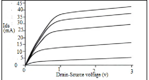
Fig -4: I-V characteristics of HEMT
[image:2.595.36.259.67.338.2] [image:2.595.323.547.382.509.2] [image:2.595.309.559.553.687.2]© 2017, IRJET | Impact Factor value: 5.181 | ISO 9001:2008 Certified Journal | Page 107
4. PROPOSED DESIGN WITH MATERIAL
COMPARISON
4.1 Si [Silicon] :
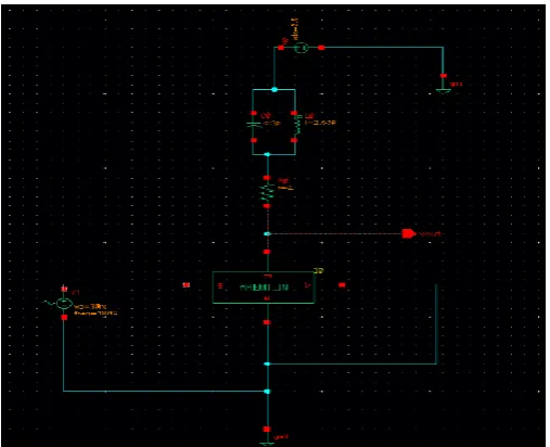
The single stage RF- Common source amplifier using Si-CMOS is designed in order to verify the operation of the device. The schematic representation and transient analysis of a CS Amplifier is shown in Fig -5 and Fig - 5.1.This amplifier is tuned to 100GHz using tuning circuit. The gain of CS amplifier drops to -9.35dB as presented in gain curve Fig- 5.2.
[image:3.595.312.557.53.247.2]Fig -5. CS amplifier using Si
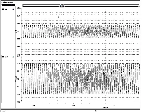
[image:3.595.37.289.259.441.2]Fig-5.1. Transient response of CS amplifier
Fig -5.2. The AC response of CS amplifier showing -9.35db
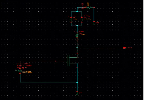
The source follower also known as common drain amplifier, the input signal is fed at the gate as in case of CS amplifier but the output is noticed at the source terminal. The schematic representation of common drain amplifier using Si is shown in Fig -6.the gain curve of the source follower is displayed in Fig -6.1. The silicon transistor works as a source follower at low frequencies when compared to CS amplifier i.e. up to 10GHz.
[image:3.595.308.562.400.566.2]Fig -6. Schematic view of source follower using Si
[image:3.595.38.287.495.692.2] [image:3.595.310.548.595.745.2]© 2017, IRJET | Impact Factor value: 5.181 | ISO 9001:2008 Certified Journal | Page 108
4.2 GaAs [gallium Arsenide]:
[image:4.595.308.562.119.325.2] [image:4.595.35.287.224.385.2]The GaAs HEMT- CS amplifier designed in Fig-7 is tuned to 100GHz. The gain remains high and is equal to 44.17dB as shown in the gain curve Fig -7.1. The transient analysis is shown in Fig -7.2. It is noticed that the output signal is slightly distorted with respect to the input signal. The GaAs HEMT common drain amplifier presented in figure8 works at high frequencies in the order of Tera hertz. The gain curve is shown in Fig -8.1
Fig - 7: CS amplifier using GaAs
Fig -7.1. AC response presenting 44.17dB
[image:4.595.311.557.378.546.2]Fig - 7.2 Transient response of CS amplifier using GaAs
Fig - 8.Source follower using GaAs
Fig - 8.1. Gain curve of source follower
4.3 GaN [gallium nitride]:
© 2017, IRJET | Impact Factor value: 5.181 | ISO 9001:2008 Certified Journal | Page 109
[image:5.595.313.555.321.500.2]Fig - 9. CS amplifier using GaN
Fig - 9.1 Transient response of CS amplifier
[image:5.595.36.290.330.490.2]Fig -9.2 Ac response of CS amplifier with gain of 16.64dB
Fig -10 Source follower using Gallium Nitride
[image:5.595.39.556.476.723.2]Fig -10.1 AC response of source follower using GaN
Table -1: comaprison of parameters obtained for the propsed CS amplifier using CMOS & HEMT
CMOS HEMT
Parameters Si GaN GaAs Operating
Frequency 100GHz 100GHz 100GHz Supply
© 2017, IRJET | Impact Factor value: 5.181 | ISO 9001:2008 Certified Journal | Page 110
5. CONCLUSIONS
The knowledge on HEMT device and the heterostructure physics provides the main idea in the analysis of the design. The operation of AlGaAs/GaAs HEMT device along with the energy band diagram is explained. With the satisfactory literature study and the thorough knowledge on HEMT, CS amplifier and source follower are constructed using Si, GaAs and GaN n-HEMT devices. CS amplifier using HEMT shows improved gain when compared to CMOS RF amplifier. With the comparison of the three materials it is noticed that GaN provides a better performance.
ACKNOWLEDGEMENT
The researchers wish to thank BMS College of Engineering, Bangalore-19 for permitting to carry out the research work in the campus and the authors are thankful to BMS College of Engineering for the support received from Technical Education Quality Improvement Program [TEQIP- II] of the MHRD, Government of India.
REFERENCES
[1] B. Razavi, “CMOS technology characterization for analogand RF design,” IEEE J. Solid-Stuie Circuits, vol. 34, pp. 268-276, Mar. 1999.
[2] Jesús A. del Alamo1, Dae-Hyun Kim1,2, Tae-Woo Kim1, Donghyun Jin1, and Dimitri A. Antoniadis1 “III-V CMOS: What have we learned from HEMTs?” Microsystems Technology Laboratories, MIT, Cambridge, MA 02139, USA; 2 Presently with Teledyne Scientific, Thousand Oaks, CA 91360;
[3] Pdf-“Physical Foundations of Solid-State Devices”By E. Fred Schubert.
[4] Mishra, Umesh K.; Parikh, Primit; Yi-Feng Wu, "AlGaN/GaN HEMTs-an overview of device operation and applications,"Proceedings of the IEEE, vol.90, no.6, pp.1022,1031, June 2002.
[5]Kevin F Brennan. “Introduction to Semiconductor devices- for computing and Telecommunication Applications”
[6]“Microwave Devices And Circuit Design” by Ganesh Prasad Srivastava, Vijay Laxmi Gupta
[7]T. R. Lenka , Member, ACEEE and A. K. Panda , “Characteristics Study of Modulation Doped GaAs/InxGa1-xAs/AlxGa1-xAs based Pseudomorphic HEMT”International
Journal of Recent Trends in Engineering, Vol 1, No. 3, May 2009
[8]Gyan Prakash Pal, Anuj Kumar Shrivastav,“High Electron
Mobility Transistor (HEMT)”- Shanti Institute of Technology,