© 2017, IRJET | Impact Factor value: 5.181 | ISO 9001:2008 Certified Journal | Page 1812
Defect detection and classification of printed circuit board using
MATLAB
Mr.M.H.Thigale
1, Shivani Gaikwad
2, Priyanka Nangare
3, Nivedita Hule
41
Mr.M.H.Thigale, Assistant Professor, Dr. D Y Patil Institute Of Engineering Management Research, Akurdi.
2
Shivani Gaikwad, Dr. D Y Patil Institute Of Engineering Management Research, Akurdi.
3
Priyanka Nangare, Dr. D Y Patil Institute Of Engineering Management Research, Akurdi.
4
Nivedita Hule,
Dr. D Y Patil Institute Of Engineering Management Research, Akurdi.
---***---Abstract -
The importance of the Printed Circuit Boardinspection process has been magnified by requirements of the modern manufacturing environment. In electronics mass production manufacturing facilities, an attempt is often to achieve 100% quality assurance. In this work Machine Vision PCB Inspection System is applied at the first step of manufacturing. In this system a PCB inspection system is proposed and the inspection algorithm mainly focuses on the defect detection and defect classification of the defects. Defect classification is essential to the identification of the defect sources. The purpose of the system is to provide the automatic defect detection of PCB and relieve the human inspectors from the tedious task of finding the defects in PCB which may lead to electric failure. We first compare a standard PCB inspection image with a PCB image to be inspected. Normalized Cross-Correlation has been used to differentiate between defective and defect free printed circuit board. Different PCBs have been inspected using normalized cross-correlation and further defected PCBs have been used for detection of all possible defects. Here we proposes a PCB defect detection and classification system using a morphological image segmentation algorithm and simple the image processing theories. The proposed algorithm group all 14 defects found on PCB into 7 Groups .The proposed algorithm involves MATLAB image processing operations such as image subtraction, logical XOR, Flood fill.
Key Words: Printed circuit board, Normalized cross
correlation, Morphological segmentation, Image processing, Defect detection, Defect classification.
1. INTRODUCTION
Visual inspection is one of the largest cost consuming
process in PCB .It also responsible for detecting various
types of defects and ensure quality assurance for all
finished product.
There are two process included in pcb inspection.
-Defect Detection
-Defect Classification.
Nowadays various algorithms are developed for PCB
defect detection some of them are Referential, Non
referential, Hybrid , Contact Method And Noncontact
Method. In this project, Defect detection and
classification is done using image processing approach
which is part of noncontact algorithm .Here we also
used normalized cross correlation which differentiate
between defective and defect free PCB . Depending on
NCC result , if pcb is defected further segmentation is
done on pcb .After segmentation ,by using arithmetic
and image processing operation we can detect defects
and classify based on similarities and area of
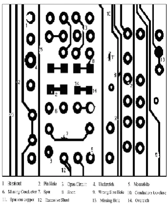
occurance. There are 14 known types of defects for
single layer, bare PCBs as shown in Table I.
2. LITERATURE SURVEY
Moganti proposed firstly three categories of PCB inspection algorithms:
1]referential approach: where comparision is made between test and reference image.
2] non-referential approaches :where general design rule verify such as width of conductor and insulator
© 2017, IRJET | Impact Factor value: 5.181 | ISO 9001:2008 Certified Journal | Page 1813 involve a combination both of referential approaches and
non-referential approaches. These approaches have the advantages of the both , but at same time they are more complex.
Heriansyah, 2012 proposed a technique that classifies PCB defects using neural network. This algorithm segments the image into basic patterns assignment, patterns normalization, and classification of the defects developed by binary morphological image processing and Learning Vector Quantization (LVQ) neural network. Here the 11 Defective patterns have been designed. The designed to test and train the neural network and this design pattern are in 8 x 8 pixels size and have the binary format.
This approach is pixel-based and classify seven defects (short, missing hole, pinhole, open, mouse-bite, spur, and etching problem). And contain few stages : segmentation, windowing (reference image and detected defects), defects detection, pattern assignment, normalization, and classification. neural network training part is done off-line, it does not affect the overall processing time.
N. K. Khalid in 2008
Propose algorithm , which implemented using Bars PCB .In this algorithm two images take such as reference and test images. The algorithm limitation is it work on only binary images can be work with grayscale but with same modification or with not accurate. After taking two image subtraction will gives directly difference, then NOT and floodfill operator using this algorithm type of defects simply converted to 5 groups.
S. H. Indera Putera, 2010
Did advance work then Khalid he made 7 groups instead of 5 groups so accuracy will increase. This is work as it combines segmentation algorithm each image segmented into 4 pattern produced 5 images for each pair of segmented image. So totally 20 new images produced. Out of which 7 is beneficial for result each group will defiantly contain one defect and maximum will be 4 defects.
B. Kaur, G. Kaur and A. Kaur: This paper presented Printed Circuit Boards (PCBs) inspection using normalized cross correlation. Correlation
Normalized Cross-Correlation is use to differentiate the defective and defect free PCB and further use defect defection techniques.
3 .DESIGN METHODOLOGY
3.1 INTRODUCTION
PCB defects can be categorized into two groups; functional defects and cosmetic defects . Functional defects can seriously affect the performance of the PCB or cause it to fail. Cosmetic defects affect the appearance of the PCB, but can also jeopardize its performance in the long run due to abnormal heat dissipation and distribution of current. There are 14 known types of defects for single layer, bare PCBs as
Shown in Table below:
[image:2.595.349.520.418.631.2]3.2 Various defects on PCB are as shown in following fig.
© 2017, IRJET | Impact Factor value: 5.181 | ISO 9001:2008 Certified Journal | Page 1814
3.3 FLOW CHART 3.4. BLOCK DIAGRAM
3.5 WORKING
A) Normalized cross-Correlation:-
Normalized cross-correlation has been used for detection whether the PCB is defective or not .NCC gets two values either 0 or 1.If NCC is equal to 1 then there is correlation between images and they are matched to each other and if NCC equal to 0 there is no correlation . when both images are same means there is no defects ,Mathematical equation for NCC is given by,
where Xi is base image and Yi is the test image.
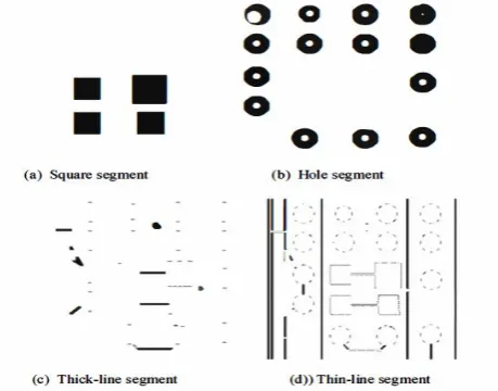
B) SEGMENTATION
© 2017, IRJET | Impact Factor value: 5.181 | ISO 9001:2008 Certified Journal | Page 1815 PCB image . Test image is which is defective PCB image.
[image:4.595.311.537.103.231.2]Which contain all 14 types of defects . both this images are segmented into 4 segments as ; square segment hole-segment, thick-line segment and thin-line segment. Where square segment consist of square pads, the hole-segment consist image of hole pads, the thick-line segment consist of image of thick conductors and the thin-line segment consist images of thin conductors.
FIG : SEGMENTATION OF IMAGES
C) THRESHOLDING
Thersholding is used to convert grayscale image into binary image. Here we consider threshold value and pixel of images compared with this threshold value . If threshold value is less than pixel intensity, then the pixel is binary one (white)or it is greater , then it is binary zero(black).
D) IMAGE PROCESSING USING ARITHMETIC
OPERATIONS:-
After getting binary image, image processing algorithms are used and this are NOT, X-OR AND IMFILL operation . After processing these algorithms we get 5 images for each 4 segmented template or test image .Thus we get 4*5 =20 images which will improve over all defect detection and classification ability of system.
1. NOT operator - NOT operator is just a complement of image that is it is used to change and image from black to white and vice varsa.
FIG : TRUTH TABLE OF NOT OPERATOR
2.IMFILL OPERATION
This operation could be useful in removing irrelevant artifacts from images. This operator is used to fill the holes in a binary image.
3.Image difference operation
[image:4.595.43.273.193.373.2]Image difference, is the simple technique which c consists of comparing both images pixel-by-pixel by XOR logic operator. Comparison operation is another name for image difference operation . Image difference operation is used to get the differences between two images. The truth table of XOR is given in Table below.
TABLE 3: TRUTH TABLE OF XOR
E)CLASSIFICATION:
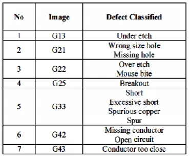
[image:4.595.311.556.319.436.2]© 2017, IRJET | Impact Factor value: 5.181 | ISO 9001:2008 Certified Journal | Page 1816 G22 and G23 from the hole segment, G33 from the thick-line
[image:5.595.44.230.160.312.2]segment and G42 and G43 from the thin line segment. The defects classified by these groups are listed in the table below-
TABLE 4:-DEFECTS CLASSIFIED
4. ADVANTAGES, DISADVANTAGES AND APPLICATIONS
ADVANTAGES
All defects are realized properly.
Classification accuracy is good.
Production cost is reduced.
Less labour cost.
Median filter is used to reduce the unwanted noise in the reference and test image of PCB.
DISADVANTAGES
All groups are unable to address the defects individually.
Image arithmatic operation algorithms requires same size of reference and test PCB image.
Algorithms do not work on loaded PCB’s.
APPLICATIONS
Industries manufacturing consumer electronics products such as mobile phones, tablet pc, automatic washing machine.
5. CONCLUSION AND FUTURE SCOPE
CONCLUSION
After the experiment, the hybrid algorithm will successfully detect and classify 13 defects into 7 groups. The limitation of this algorithm will be that some groups are unable to address each defect individually. Future improvement for the algorithm should include the ability to detect and classify all 14 defects individually.
FUTURE SCOPE
Due to large use of PCB in anywhere it should be defect free if it contain defects it will no more working state and all cost will be wasted so, in future this algorithm will very imp to overcome PCB fault due to defects.
6. REFERENCES
[1] R. Heriansyah , S.A.R AI-Attas , and M.M. Ahmad Zabidi,
'Segmentation of PCB Images into Simple Generic Patterns using
Mathematical Morphology and Windowing Technique', Co GRAMM
Melaka, Malaysia 2002
[2] S. H. Indera Putera and Z. Ibrahim (2010.)‘Printed Circuit Board Defect Detection Using Mathematical Morphology and MATLAB Image Processing Tools’, ICINT
2010, Shanghai, China
[3] N. K. Khalid, Z. Ibrahim, M. S.Z. Abidin (May 2008) An algorithm to group defects on printed circuit board for automated visual inspection. IJSSST, Vol. 9, No. 2, ISSN: 1473-804x]
[4] M. Moganti, F. Ercal, C. H. Dagli and S. Tsunekawa (1996), Automatic PCB inspection algorithms: A survey,
Computer Vision and Image Understanding, vol.63, no.2.