Comparative Analysis of Low Power 10T and 14T Full
Adder using Double Gate MOSFET at 45nm Technology
Anuj Kumar Shrivastava
Research Scholar ITM University Gwalior M.P. IndiaShyam Akashe
Associate Professor ITM University Gwalior M.P. IndiaABSTRACT
Full adder is the basic block of arithmetic circuit found in microcontroller and microprocessor inside arithmetic and logic unit (ALU). Improving the performance of the adder is essential for upgrade the performance of digital electronics circuit where adder is employed. This paper described a comparative analysis of double gate 10T and double gate 14T adder at 45nm technology. In this paper we calculate the leakage current, average power and Delay of the designed circuit of 10T and 14T Full adder. 10T double gate full adder achieves 31.25% reduction in active power and 95% reduction in leakage current as compared to 14T double gate full adder. Simulation results of double gate full adder have been performed on cadence virtuoso tool with 45nm technology.
Keywords
Full adder, Low power, arithmetic operation, Double gate mosfet, leakage current.
1.
INTRODUCTION
The adder is one amongst the foremost necessary elements of a processor and DSPs as a result of it's employed in ALU [1] [2]. Increasing the demand of portable physical science device such as PDA, Mobile Phones, portable computer needs the utilization of power economical circuits. The efficiency of ALU is set by the efficiency of adder circuit. Several structures are designed to upgrade the performance of adder unit in terms of low power and high-speed and are a lot of essential [3].
The power consumption for CMOS circuit is given by the following equation:
Pavg = Pdynamic + Pleak + Pshort-circuit
= CLVddVfclk + IleakVdd +IscVdd (1)
We clearly say that the power depend on the different parameter as well as on the supply voltage. Lowering the supply voltage would significantly lower the power consumption of the circuit. This basic concept of would be used to improve the performance of adder circuit.
2.
FULL ADDER
Full adder is a combinational circuit that performs the addition operation of 3 input bits. It basically consists three inputs and two outputs. The input variables are expressed by A, B and Cin. The two output variables are expressed by
sum(S) and carry (Cout) [4]. Fig. 1 shows the essential block
diagram of full adder cell. The Boolean expression for full adder operation is defined below:
SUM = A ⊕ B ⊕ Cin
(2)
Cout = AB + A ⊕ B Cin
(3)
Fig.1. Block Diagram of basic full adder circuit
2.1
USING DOUBLE GATE 10T FULL
ADDER CIRCUIT
Double gate MOSFET will be constructed by connecting two transistors in parallel as a way that their supply and drain are connected together. Double gate MOSFET can be classified in two types, based on biasing of gate. Once the front and back gate area unit connected along, initial kind is achieved and it is referred as three terminal devices. This device is used for direct replacement of single gate transistor. Second kind is achieved by independent gate control [5] [6].
Fig.2. Double Gate Full Adder.
In this section one bit full adder circuit is presented by using double gate transistors for improve the performance of adder
C B
A
Cout
Sum
Cin B A
S
in terms of power and leakage. Fig. 2 shows the double gate 10T full adder circuit. This cell is made by using the 4T XOR gate. It is the essential component of full adder cell and generates the essential addition operation of adder cell. It behaves like a single half adder cell. Conventionally XOR gate use 8 MOSFETs for proper working, but present we have different topologies [7] [8]. Here we have used 4T XOR gate to increase circuit density. Fig.3 shows the 4T XOR gate. Using this XOR gate, reduction in size of full adder is achieved and overall leakage is also reduced [9] [10]. The schematic of full adder is shown in fig.2 and output waveform is shown in fig.4
Fig.3. Schematic of 4T XOR
Fig.4. Output Waveform of Double Gate Full Adder.
2.2
DOUBLE GATE 14T FULL ADDER
CIRCUIT
in terms of power and leakage using 14 transistors. Fig. 5 shows the double gate 14T full adder circuit. This cell is constructed by using the 4T XOR gate. It is the essential element of full adder cell and it generates the basic addition operation of adder cell. It behaves like a single half adder cell. In the 14T full adder cell we used two 4T XOR gate. Conventionally XOR gate use 8 MOSFETs for proper working, but present we have different topologies. Here we have used 4T XOR gate to increase circuit density [11] [12]. Using this XOR gate, reduction in size of full adder is achieved and overall leakage is also reduced. Output waveform of 14T full adder is shown in fig.6.
Fig.5. Double Gate 14T Full Adder.
Fig.6. Output Waveform of Double Gate Full Adder. Sum
Cout
Cin B
A
A xor B
3.
SIMULATION AND RESULT
A single bit full adder circuit based on double gate MOSFET technique is proposed. Simulation of the proposed circuit is done by using the Cadence virtuoso tools. It is used for measurement of leakage, power consumption and delay of the proposed circuit at 45nm technology with different supply voltage from 0.7v to 1.0v.
3.1
LEAKAGE CURRENT
Leakage is a quantum phenomenon where mobile charge carrier tunnel through an insulating region. Leakage increases as the thickness of the insulating region is decreases. Tunneling leakage can also occur across junctions between heavily doped p-type and n-type. The basic equation of leakage current is shown in Eq.4 [11] [13].
I
leakage= I
sub+ I
ox(4)
Where, Isub = sub-threshold leakage current, Iox = gate-oxide leakage current.
I
sub= K
1W e
−V tn Vθh(1 − e
−VVθ
)
(5)
Where, K1 and n are experimentally derived, W = gate width, Vth = threshold voltage, n = slope shape factor, Vθ = thermal voltage.
I
ox= K
2W (
TVox
)
2
e
−αToxV6)
Where, K2 and α are derived experimentally, Tox = oxide thickness.
Table 1. Leakage current at difference voltages of 10t and 14t full adder
Voltage 10T Full Adder (pA) 14T Full Adder (pA)
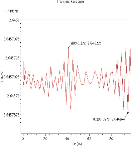
0.7 2.646 46.6
0.8 2.915 76.36
0.9 3.165 122
[image:3.595.317.538.76.575.2]1.0 3.401 190
[image:3.595.323.528.81.293.2]Fig.7. Leakage Current Waveform of Double Gate 14T Full Adder at 0.7V
Fig.8. Leakage Current Waveform of Double Gate 10T Full Adder at 0.7V
[image:3.595.321.533.337.572.2]3.2
ACTIVE POWER
At the time of operating the power is dissipated by the circuit is known as active power. Active power includes both static power and dynamic power of the circuit. The basic equation of active power is shown in Eq. (7) [14].
𝑃
𝑎𝑐𝑡𝑖𝑣𝑒= 𝑃
𝑑𝑦𝑛𝑎𝑚𝑖𝑐+ 𝑃
𝑠𝑡𝑎𝑡𝑖𝑐(7)
= 𝑃
𝑠𝑤𝑖𝑡𝑐 𝑖𝑛𝑔+ 𝑃
𝑠𝑜𝑟𝑡 −𝑐𝑖𝑟𝑐𝑢𝑖𝑡+ 𝑃
𝑙𝑒𝑎𝑘𝑎𝑔𝑒= 𝛼
0→1× 𝐶
𝑙× 𝑉
𝑑𝑑2× 𝑓
𝑐𝑙𝑘+
𝐼
𝑠𝑐× 𝑉
𝑑𝑑+ 𝐼
𝑙𝑒𝑎𝑘𝑎𝑔𝑒+ 𝑉
𝑑𝑑(8)
Where, Cl = load capacitance, fclk = clock frequency, α = switching activity, Isc = short circuit current, Ileakage = leakage current, Vdd = supply voltage.
Table 2. Active power at difference voltages of 14t full adder
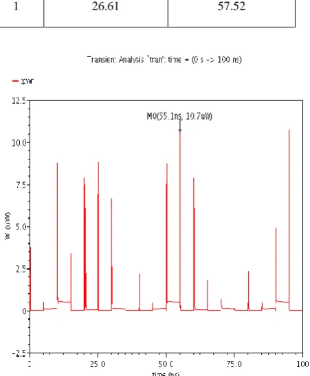
Voltage 10T Full Adder(µW) 14T Full Adder (µW)
0.7 7.34 10.7
0.8 13.21 20.56
0.9 18.95 36.69
[image:4.595.321.526.85.283.2]1 26.61 57.52
Fig.9. Active Power Waveform of Double Gate 14T Full Adder at 0.7V
[image:4.595.52.280.118.681.2]Fig.10. Active Power Waveform of Double Gate 10T Full Adder at 0.7V
Table 2 shows the active power of 10T and 14T full adder cell using double gate MOSFET at different supply voltage. Fig 9 and fig 10 shows the active power waveform of double gate 14T and 10T full adder cell at 0.7V.
3.3
DELAY
Propagation delay is the required by a digital signal to travel from that input of the circuit to the output. The propagation delay is inversely proportional to the speed of the architecture and hence it is important performance parameter. The basic equation of delay in presence of sleep transistor is shown in Eq. (9) [13]
𝑑
𝑠𝑙𝑒𝑒𝑝𝑖=
𝐾𝐶𝐿𝑉𝑑𝑑(𝑉𝑑𝑑− 2𝑉𝑥−𝑉𝑡𝐿)𝛼
(9)
[image:4.595.57.283.342.616.2]Where, where Vx is the potential of the virtual rails, and K is the proportionality constant, CL is the load capacitance at the gate output; VtL is the low-voltage threshold. Fig.11 shows the Delay Comparison Graph for double gate 10T and 14T full adder cell.
Fig.11 Delay Comparison Graph of 10T and 14T Full Adder Circuit.
171.3
126.8 92.68
68.3 151
55.54
14.845.18 0
50 100 150 200
0.7 0.8 0.9 1
D
e
lay
(
p
s)
Voltage (V)
10T FA
[image:4.595.315.545.539.705.2]4.
CONCLUSION
The analysis in this paper has been carried out while analyzing both lOT and 14T full adders individually and comparing them on the basis of calculation of active power, leakage current and delay by varying different parameters. The outcomes of the simulation show that lOT full adder to be a better option with improved performance over 14T structure. As compare to 14T double gate full adder active power of 10T full adder is reduced from 10.7µW to 7.34 µW at 0.7V. As compare to 14T double gate full adder Leakage current of 10T full adder is reduced from 10.7µW to 46.6pA to 2.646pA at 0.7V.As compare to 10T double gate full adder Delay of 14T double gate full adder is reduced from 171.3ps to 151ps.
5.
REFERENCES
[1] Sun, X.-G., Mao, Z.-G., and Lai, F.-C. “A 64 bit parallel CMOS adder for high performance processors”, Proc. IEEE Asia-Pacific Conf. on ASIC, 2002, pp. 205–208. [2] Vahid Moalemi and Ali Afzali-Kusha, “Subthreshold
1-bit Full adder cells in sub-100nm technologies”, IEEE Computer Society Annual Symposium on VLSI (ISVLSI-07), Porto Alegre, Brazil, March 9-11, 2007 (ISBN 0-7695-2896-1).
[3] Lu Junming; Shu Yan; Lin Zhenghui; Wang Ling," A Novel IO-transistor Low-power High-speed Full adder cell", Proceedings of 6th International Conference on Solid-State and Integrated-Circuit Technology, vol-2, pp. 1155-1158,2001.
[4] Dan Wang, Maofeng Yang, Wu Cheng, Xuguang Guan, Zhangming Zhu, Yintang Yang, "Novel Low Power Full Adder Cells in 180nm CMOS Technology", 4th IEEE Conference on Industrial Electronics and Applications, ICIEA 2009, pp 430-433.
[5] Adarsh Kumar Agrawal, Shivshankar Mishra, and R K. Nagaria, "Proposing a Novel Low-Power High-Speed Mixed GDI Full Adder Topology", accepted in Proceeding of IEEE International Conference on Power, Control and Embedded System (ICPCES), 28 Nov.-1 Dec. 2010.
[6] Shipra Mishra, Shelendra Singh Tomar and Shyam Akashe, “Design low power 10T full adder using process and circuit techniques”, 7th IEEE International Conference on Intelligent Systems and Control(ISCO) Coimbatore 2013, pp. 325-328.
[7] Mohammad Hossein Moaiyeri and Reza Faghih Mirzaee, Keivan Navi, 'Two New Low-Power and High-Performance Full Adders", Journal Of Computers, Vol. 4,N o. 2,February 2009.
[8] Mariano Aguirre-Hernandez and Monico Linares-Aranda, "CMOS Full Adders for Energy-Efficient Arithmetic Applications", IEEE Transactions On Very Large Scale Integration (Vlsi) Systems, Vol. 19, No. 4, April 2011.
[9] G.Shyam Kishore, Associate.Prof, ECE dept, JITS, Karimnagar, Andhra Pradesh, India, "A Novel Full Adder with High Speed Low Area", Proceedings published in International Journal of Computer Applications® (UCA) , 2nd National Conference on Information and Communication Technology (NCICT) 2011.
[10]R. Johri, R. Singh, S.P. Pandey and S. Akashe, “Comparative analysis of 10T and 14T full adder at 45nm technology”, 2nd IEEE International Conference on Parallel Distributed and Grid Computing (PDGC) Solan 2012, pp. 833-837.
[11]Neil H. E. Weste, David Harris and Ayan Banerjee, “CMOS VLSI Design: A Circuit and System Perspective”, Pearson Education, Third Edition 2011. [12]Vahid Moalemi and Ali Afzali-Kusha, “Subthreshold
1-bit Full adder cells in sub-100nm technologies”, IEEE Computer Society Annual Symposium on VLSI (ISVLSI-07), Porto Alegre, Brazil, March 9-11, 2007 (ISBN 0-7695-2896-1).
[13]K. Roy, S. Mukhopadhyay and H. Mahmoodi-Meimand, “Leakage Current Mechanisms and Leakage Reduction Techniques in Deep-Submicron CMOS Circuits”, Proceedings of the IEEE 2003, Vol. 91, No. 2, pp. 305-327.