PERFORMANCE OF DEFECTED GROUND STRUCTURE FOR RECTANGULAR MICROSTRIP PATCH ANTENNA
JAMAL MUHIYADIN SH-ALI
This thesis is submitted as partial fulfillment of the requirements for the award of the Master Degree of Electrical Engineering.
Faculty of Electrical and Electronic Engineering, Universiti Tun Hussein Onn Malaysia
ABSTRACT
In wireless communications systems, harmonics and unwanted frequency other than designed one becomes a dominant factor in limiting quality and capacity of transmitted or received signal. Rectangular microstrip patch antenna (RMPA) is designed in order to obtain the required parameter responses at 2 GHz. The proposed antenna is excited through the microstrip feed line which is connected directly to the patch antenna. RMPA of length 35.8462 mm and width 46.0721 is designed on the substrate dielectric material FR-4 having dielectric constant r=4.3 and thickness 1.6 mm. The defect ground structure (DGS) has gained much attention over the last few years for its ability to increase the performance of wireless system by effectively suppressing harmonics DGS shows a better result compared to the conventional antenna. It effectively suppressing spurious frequency and reduces the amplitude of the unwanted multiple bands since the antenna radiates only one resonating frequency.
ABSTRAK
CONTENTS
CHAPTER TITLE PAGE
TITLE i
DECLARATION ii
DEDICATION iii
ACKNOWLEDGEMENT iv
ABSTRACT v
ABSTRAK vi
TABLE OF CONTENTS vii
LIST OF TABLES xi
LIST OF FIGURES xii
LIST OF ABBREVIATIONS AND SYMBOLS xiv
LIST OF APPENDICES xvi
I INTRODUCTION 1
1.1 Back ground of Study 1-2
1.4 Scopes of Study 4
1.5 Outlines 5
II LITERATURE REVIEW 6
2.1 Introduction 6
2.2 Antenna theory 6 2.2.1 Antenna Definition 7-8 2.3 Basic operation 8
2.4 Antenna Parameters 9
2.4.1 Radiation Pattern 9
2.4.2 Directivity 9 2.4.3 Gain 9-10 2.4.4 Input Impedance 10 2.4.5 Bandwidth 10
2.4.6 Return Loss 11
2.4.7 Voltage Standing Wave Ratio (VSWR) 11
2.5 Feeding Techniques 11
2.5.1 Aperture coupling 12
2.5.2 Proximity coupling 13
2.6 Types of antenna 15-17 2.7 Substrate 17 2.8 Defected Ground Structure 18-21 2.9 Application of DGS 21-24 2.94 Review of previous work 25-26
III METHODOLOGY 27
3.1 Introduction 27
3.1.1 Procedures of development of the project 28-29 3.2 Design process for RMPA 30
3.3 Design Equation 30
3.4.1 Design consideration for RMPA 31-37
IV RESULTS AND ANALYSIS 38
4.1 Introduction 38-39
4.2Design RMPA in CST 39
4.6 Results of Equivalent circuit modeling for DGS 46-48
4.6.1Dumbbell DGS with transmission line 48
4.6.2 Rectangular DGS with transmission line 49
4.6.3 Circular DGS with transmission line 49
4.6.4 Boundary condition 50
4.7. Rectangular slot 51
4.7.1 Influence of the slot width 51-52 4.7.2 Influence of the slot length 52-54 4.7.3 Square head slot 54
4.7.3.1 Influence of the square head dimension 54-55 4.7.3.2 Influence of the slot width 55-56 4.7.3.3 Influence of the slot length 57-58 4.7.4 Dumb-bell slot 58
4.7.4.1 Influence of the Dumb-bell slot head dimension 58-59 4.7.4.2 Influence of the slot width 59-60 4.7.4.3 Influence of the slot length 60-61 4.8 Simulation result 64-69 4.9 Simulation result analysis 70
4.13 Measured result analysis 80 4.14 Comparison between simulated and measurement result
of RMPA at 2 GHz 81
V CONCLUSION AND RECOMMENDATION 83 5.1 Conclusion 83-84 5.2 Recommendations for Future Work 84
REFERENCES 85-88
APPENDICES 89-91
LIST OF TABLES
NO. OF TABLE TITLE PAGE
3.1 Parameter of antenna 30 3.2 Calculated parameters 33 3.3 Optimization dimension of proposed RMPA 34 4.1 Rectangular slot characteristics for different
slot width 51 4.2 Rectangular slot characteristics for different
slot length 53 4.3 Square head slot characteristics for different
slot head length 54 4.4 Square head slot characteristics for different
slot width 56 4.5 Square head slot characteristics for different
slot length 57 4.6 Dumb-bell slot characteristics for different
4.7 Dumb-bell slot characteristics for different
slot width 60 4.8 Dumb-bell slot characteristics for different
LIST OF FIGURES
NO. OF FIGURE TITLE PAGE
2.1 Transmitting and receiving antenna structure 7 2.2 Aperture coupled feed patch antenna 12 2.3 Proximity coupled feed patch antenna 13 2.4 Microstrip line feed patch antenna 14 2.5 Coaxial probe feed patch antenna 15 2.6 Basic configuration RMPA with feed line 16
2.7 Radiating Patch 17
2.8 Isometric view of dumbbell shell shaped DGS 18 2.9 Distribution of surface current on the Ground Plane
of a unit cell DGS 19 2.10 Truncated structure according to distribution current on surface
ground plane 19
2.11 Some resonant structures used for DGS application 20 2.12 Defected ground structure for microstrip line 22 2.13 Dumb-bell shaped DGS 23
2.14 DGS unit cell 23
3.2 Project 2 flow chart 29
3.3 Flowchart based procedure for RMPA 31
3.4 Microstrip calculator 35
4.1 CST schematic conventional for RMPA 39
4.2 Returnloss vs Frequency of conventional RMPA without DGS 40 4.3 Geometry design of RMPA with DGS Microstrip Patch antenna41 4.4 Return loss vs Frequency of RMPA with DGS 41
4.5 Comparison of Returnloss vs frequency with and without DGS 42 4.6 Bandwidth for conventional RMPA without DGS 43
4.7 Bandwidth for RMPA with DGS 44
4.8 Shapes of DGS slot 45
4.9 Equivalent Circuit of DGS 46
4.10 Response of the proposed DGS 47
4.11 Designed Equivalent Circuit of DGS using Multisim 47
4.12 Simulated result of DGS using Multisim software 48
4.13 Dumbbell DGS with transmission line 48
4.14 Rectangular DGS with transmission line 49
4.15 Circular DGS with transmission line 49
4.16 Boundary condition 50
4.17 Wire frame view of the rectangular DGS slot 51
slot length 53
4.20 Square head slot 54
4.21 Simulated S-parameter of square head slot for different head length 55
4.22 Simulated S-parameter of square head slot for different slot width 56
4.23 Simulated S-parameter for square head slot for different slot length 57
4.24 Wire frame view of the Dumb-bell DGS slot 58
4.25 Simulated S-parameters for Dumb-bell slot for different slot radius 59
4.26 Simulated S-parameter for dumb-bell slot for different slot width 60
4.27 Simulated S-parameter for dumb-bell slot for different slot length 61
4.28 RMPA with square head DGS slot 62
4.29 RMPA with rectangular DGS slot 62
4.30 RMPA with circular DGS slot 63
4.31 Simulated 3-D radiation pattern of conventional RMPA 64
4.32 Simulated smith chart of conventional RMPA 64
4.33 Simulated VSWR of conventional RMPA 64
head DGS slot 65
4.36 Simulated VSWR of RMPA with square head DGS slot 65
4.37 Simulated 3-D radiation pattern of conventional RMPA with rectangular slot 66
4.38 Simulated smith chart of RMPA with rectangular slot 66
4.39 Simulated VSWR of RMPA with rectangular slot 66
4.40 Simulated 3-D radiation pattern of conventional RMPA with circular head slot 67
4.41 Simulated smith chart of RMPA with circular head slot 67
4.42 Simulated VSWR of RMPA with circular head slot 67
4.43 2D radiation pattern of pattern of conventional RMPA 68
4.44 2D radiation pattern of pattern of RMPA with square head DGS slot 68
4.45 2D radiation pattern of pattern of RMPA with rectangular slot 69
4.46 2D radiation pattern of pattern of RMPA with circular head slot 69
4.47 Measured S-parameter (S1,1) of conventional RMPA 72
4.48 Measured Smith chart of conventional RMPA 72
4.49 Measured VSWR of conventional RMPA 73
4.50 Measured S-parameter (S1,1) of rectangular DGS slot for RMPA 73
4.51 Measured Smith chart of rectangular DGS slot for RMPA 74
4.52 Measured VSWR of rectangular DGS slot for RMPA 74
4.53 Measured S-parameter (S1,1) of square head DGS slot for RMPA 75
4.54 Measured Smith chart of square head DGS slot for RMPA 75
4.56 Measured S-parameter (S1,1) of Circular head DGS slot
for RMPA 76 4.57 Measured Smith chart of Circular head DGS slot for RMPA 77 4.58 Measured VSWR of Circular head DGS slot for RMPA 77
4.59 Comparative graph between simulated and measurement result for conventional RMPA 78
4.60 Comparative graph between simulated and measurement result for rectangular slot DGS 78
4.61 Comparative graph between simulated and measurement result for
square head DGS slot 79 4.62 Comparative graph between simulated and measurement result for
circular slot DGS 79 4.63 Photograph of Fabricated RMPA with Rectangular DGS slot 81 4.64 Photograph of Fabricated RMPA with square head DGS slot 82 4.65 Photograph of Fabricated RMPA with Circular head DGS slot 82
LIST OF ABBREVIATION AND SYMBOLS
EM Electromagnetic
CST Computer Simulation Technology
λ Wave Length
RMPA Rectangular Microstrip Patch Antenna
MPA Microstrip Patch Antenna
RL Return Loss
L Length
W Width
GP Ground Plane
FR-4 Flame Retardant 4
r Dielectric Constant
VSWR Voltage Standing Wave Ratio
BW Bandwidth
h Substrate Thickness
DGS Defected ground structure
Fl Lower frequency
Fc Cut off frequency
Fo Operating frequency
LIST OF APPENDICES
APPENDIX TITLE PAGE
A Gantt chart for PSM I 89
B Gantt chart for PSM II 90 C VITA 91
CHAPTER I
INTRODUCTION
1.1 Background of Study
Wireless technology provides less expansive equipment’s and flexible way for communication purpose. Antenna has its own importance in communication systems; it provides radiation of electromagnetic energy uniformly in all directions. Antenna is a transducer, which converts one form of energy in to another. Here it is designed to transmit or receive electromagnetic waves from one source to destination. Microstrip antennas have several advantages over other conventional microwave antennas and therefore widely used in many practical applications.
A large number of microstrip patches to be used in wireless applications have been developed. [1-3].
A conventional microstrip antennas consist of a pair of parallel conducting layers separating a dielectric medium, referred as substrate. In this configuration, the upper conducting layer or “patch” is the source of radiation where electromagnetic energy fringes off the edges of the patch and into the substrate. The lower conducting layer acts as a perfectly reflecting ground plane, bouncing energy back through the substrate and into free space [4].
Rectangular microstrip patch antenna can be fed by using coaxial probe or microstrip line edge feed. In this project, the method of feeding is microstrip edge feed where the transmission line is being printed along with the patch antenna.
The patch antenna usually has spurious frequency and to overcome this Defected Ground Structure (DGS) on the ground plane of the transmission is made. The DGS at the ground of the transmission line acts like a low pass filter which will determine the frequency that can be passed through the transmission line.
Recently, both defected ground structure (DGS) and electromagnetic band gap (EBG) have received much attention because of their use in radar, satellite, microwave areas and mobile communication systems. Such systems often require circuits to be as small as possible. The DGS components are the dominant technology which can provide size reduction and has the capability of harmonics and spurious suppression.
The DGS is realized by etching a certain pattern in the backside metallic plane which perturbs the current distribution in the ground, and hence increases the effective inductance and capacitance of the microstrip line. Therefore, a DGS cell is equivalent to an LC circuit.
The square dimension of the DGS represents the inductor and the narrow lattice is the capacitor. The value of the inductor and the capacitor will affect the cut off frequency of the filter that is produce by the DGS.
1.2 Problem Statement
The regular microstrip patch antenna usually has spurious frequency which can make the signal at the operating frequency corrupt, spurious becomes a dominant factor in limiting quality and capacity.
In order to suppress the spurious frequency, it can be achieved by adding either low pass or band pass filter that can be used to reject the spurious frequency. By using this method, it can increase the cost of the antenna.
The Defected Ground Structure (DGS) has gained much attention over the last few years for its ability of effectively suppressing spurious frequency. To overcome that problem, it is proposed to use DGS which is being used at the transmission line for the patch antenna, because it is easy to design and fabricate.
The simulation of the antenna will be done in CST software.
1.3 Objectives of Study
To design rectangular patch antenna with DGS which operating at the resonant frequency at 2 GHZ.
To compare the influence of DGS performance and conventional patch antenna.
1.4 Scopes of Study
The scope this project is mainly divided in two parts: i. Project I
Calculation
Simulation ii. Project II
Fabrication
Testing
The scope of this project is to design and fabricate microstrip patch antenna with DGS. The designed antenna must suppress any spurious frequencies other than the designed frequency. Besides that to explore and simulate the basic parameters of rectangular patch antenna using CST microwave Studio software.
1.5 Report outlines
This thesis is organized into five chapters. The first Chapter 1, it will cover on introduction on the whole thesis. It also includes the objectives, problem statements, scope of works and main introduction of the project.
Chapter 2 explains on the literature review of the project. The literature review begins with the introduction, followed by antenna parameters. Introduction is an explanation on the overview of the literature. As for the antenna topic, it is about the general description of an antenna. It is also cover on the basic principal of the antenna. This project is more focusing on Rectangular microstrip patch antenna. It is important to recognize the parameter of the antenna before designing the antenna itself.
Chapter 3 describes project methodology where it is focusing on the method that used to complete the project accordingly. The methodology will be presented in the flowchart which clearly explained about how this project is planned and organized in completing the
project.
Chapter 4 presents the result for the system designed and discussion of overall result. The conclusion and recommendation of this project will be discussed in chapter 5.
CHAPTER II
LITERATURE REVIEW
2.1 Introduction
This chapter reviews several related previous work. Literature review is significant part for understanding the specification characteristics to model microstrip patch antenna. Literature review is one of the processes of developing rectangular patch antenna with DGS which operates at the resonant frequency 2 GHZ, for this project. The literature review explains on the antenna and the basic antenna operation, basic antenna parameter, the feed technique.
2.2 Antenna Theory
2.2.1 Antenna definition
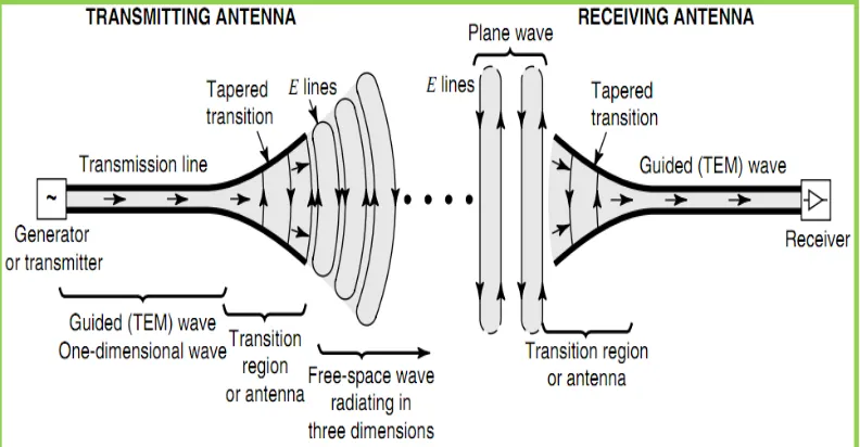
certain desired pattern of distribution in space. Lastly it capable of receiving or transmitting electromagnetic energy over specified frequency range [1,10]. This process is described in Figure 2.1.
Figure 2.1: Transmitting and receiving antenna structure.
The guiding device or transmission line may take the form of a coaxial line or waveguide, and it is used to transport electromagnetic (EM) energy from the transmitting source to the antenna or from the antenna to receiving antenna.
In other words antenna is a device, which is used for sending and receiving the electromagnetic wave for the communication. The antenna is device that builds in the air of effectively radiating electromagnetic wave for the purpose of wireless communication. It is also effectively maintaining the electromotive force by electromagnetic wave.
system, antenna converts electrical energy which is travelling along a transmission line into electromagnetic waves. At the receiver end, an antenna converts electromagnetic waves into electrical energy on a transmission line.
2.3 Basic antenna Operation
It is apparent that the size of an antenna is inversely proportional to frequency. A relatively small antenna can efficiently radiate high frequency electromagnetic waves. As for the low frequency waves, it require relatively large antennas.
2.4 Antenna parameters
To describe the performance of antenna, the definitions of various parameters are necessary. Here the most important parameters are discussed in the following paragraph and explained how it relate to the antenna’s performance [1, 9].
2.4.1 Radiation Pattern
A radiation pattern defines the variation of the power radiated by an antenna as a function of the direction a way form the antenna, it gives the power that is radiated or received by a transmitting antenna or by a receiving antenna, respectively. In other words it is a mathematical function or a graphical representation of the radiation properties of the antenna as function of space coordinates. The radiation pattern is determined in the far-field region and is represented as a function of the directional coordinates.
2.4.2 Directivity
Directivity is a fundamental antenna parameter. It is the ratio of the radiation intensity in a given direction from the antenna to the radiation intensity averaged over all directions. The average radiation intensity is equal to the total power radiated by the antenna divided by 4π. In other words it is the ability of the antenna to focus energy in particular direction.
2.4.3 Gain
concentrate energy through a direction to give a better picture of the radiation performance. What we want is the maximum gain, which is the gain in the direction in which the antenna is radiating most of the power.
2.4.4 Input Impedance
Input impedance is the impedance presented by an antenna at its terminals or the ratio of the voltage to current at a pair of terminals. If the input impedance of the transmission line and antenna are matched, maximum power transfer will be achieved. If is not matched it will cause reduction on overall system efficiency. This is because reflected wave is generated at the antenna terminal and it will travel back towards the energy source.
For this parameter, the input impedance must match the characteristics impedance of transmission line in order to achieve maximum energy transfer between transmission line and patch. If the input impedance not matches to each other, reflected wave will be generated at antenna terminal and travel back towards the energy source. Reflection of energy results in a reduction in the overall system efficiency. If the antenna is used to transmit or receive energy, then only this loss efficiency will be occurred.
2.4.5 Bandwidth
2.4.6 Return Loss (RL)
RL is a parameter which indicates or measure of impedance match quality. When the load is mismatched the whole power is not delivered to the load there is a return of the power and that is called loss, and this loss that is returned is called the RL. If the indication of the RL is lower than -10 dB it means this matching is good, for ideal matching between the transmitter and the antenna, Г=0 and RL=∞ which means no power would be reflected back, whereas a Г=1 has RL=0dB, which implies that all incident power is reelected
2.4.7 Voltage Standing Wave Ratio (VSWR)
VSWR measures the ratio of the amplitude of the maximum standing wave to the minimum standing wave. In other words it is an indication of how good the impedance matching quality is for an antenna, the smaller the VSWR is, and the better the antenna is matched to the transmission line and more power delivering to the antenna. Typically desired value of VSWR to obtain a good impedance match is 2.0 or less (≤2).
2.5 Feeding Techniques
A feedline is used to excite and radiate by direct or indirect contact. There are many different techniques of feeding and four most popular techniques are coaxial probe feed, microstrip line, aperture coupling and proximity coupling [10].
the RF power is fed directly to the radiating patch using connecting element such as microstrip line. The microstrip and coaxial probe are examples of contacting method.
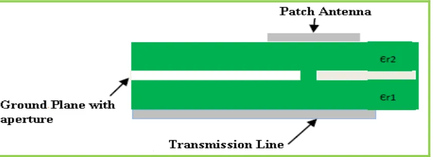
2.5.1 Aperture coupling
[image:30.595.113.535.476.629.2]Aperture coupled feed consist of two different substrate separated by a ground plane. On the bottom side of lower substrate there is a microstrip feed line whose energy is coupled to the patch through a slot on the ground plane separating two substrates. This arrangement allows independent optimization of the feed mechanism and the radiating element. Normally top substrate uses a thick low dielectric constant substrate while for the bottom substrate; it is the high dielectric substrate. The ground plane, which is in the middle, isolates the feed from radiation element and minimizes interference of spurious radiation for pattern formation and polarization purity. This is the most difficult feeding among all types because multi-layer fabrication is required and it possesses a narrow bandwidth. The antenna element is formed by two dielectric substrate layers separated in the middle by a group planed on. The radiating patch element is photo etched on the upper substrate and this is known as antenna substrate.
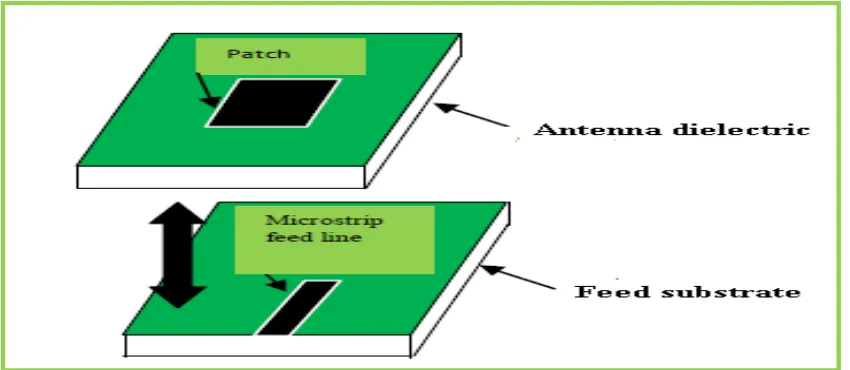
2.5.2Proximity coupling
Proximity coupling or electromagnetic coupling can be achieved by two methods. The first method is by creating a small gap between the patch and the feed line on the same substrate layer. The second method is by placing the patch and the feed line at different layers. Proximity coupling has the largest bandwidth, and low spurious radiation. However fabrication is difficult. Length of feeding stub and width-to-length ratio of patch is used to control the match. Its coupling mechanism is capacitive in nature.
[image:31.595.106.531.333.518.2]The major disadvantage of this feeding technique is that it is difficult layer that need proper alignment, also increase in overall thickness of the antenna.
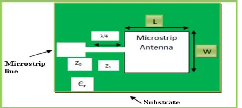
2.5.3 Microstrip transmission line
[image:32.595.109.517.258.441.2]Microstrip line is easy to fabricate, simple to model and match by controlling the inset cut position in the patch. For this project line feed was used as feeding technique because it allows the user to control the impedance match between feed and antenna.
Figure 2.4: Microstrip line feed patch antenna
2.5.4 The coaxial probe feed
This method is widely used because of its simplicity in fabrication and matching and it has low radiation. The inner conductor of the coaxial is attached to the radiation patch while the outer conductor is connected to the ground plane.
Figure 2.5: Coaxial probe feed patch antenna
2.6 Types of Antenna
For the past few decades there are several antennas which were developed. These are: Horn antennas, aperture antennas, reflector antennas, travelling wave and broadband antennas and microstrip antennas [1].
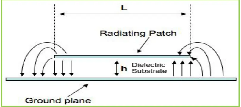
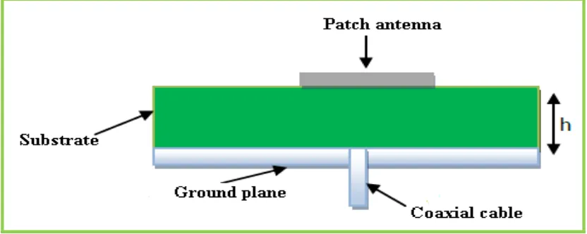
However, in this project, microstrip patch antennas will be discussed. Figure-2.3 shows a rectangular microstrip patch antenna, consists of four major parts: conductive patch, ground plane, substrate and feeding line. Conductive patch and ground plane are usually made from same material (such as copper of high conductivity). Material of the substrate and its thickness are also important. Type of the substrate has its significant role in determination of antenna dimensions. Substrate of high permittivity results in larger dimension of patch antenna. In this project FR-4 is selected for substrate, it has relative permittivity equals to 4.3.
Substrate is above the ground and conductive patch is on top of the substrate (as shown in figure-2.6). Excitation of patch is accomplished via feed line. When the patch is excited by feed, bottom of the patch at a certain point in time will have positive charge distribution and ground plane will have negative charge distribution.
Attractive forces between these two charges will hold most of them on bottom surface of the patch and top surface of ground. On the patch surface repulsive charges within the same polarity, tend to push some of charges towards edge. These charges create fringing effects and cause radiation.
The patch is generally made of conducting material such as copper or gold and can take any possible shape.
[image:34.595.117.507.465.638.2]However the main focus will be on studying the general properties of patch antennas by using rectangular patch antenna.
Figure 2.7: Radiating patch
A microstrip patch antenna is simply a radiating patch on one side of a
dielectric substrate and a ground plane on the other side. The load attaches to a
microstrip which connects the antenna's radiating patch to its ground plane.
Microstrip patch antennas radiate due to the fringing fields created between
the patch and the ground plane and resonate according to the dimensions of the
radiating patch as shown in Figure 2.7.
2.7 Substrate
2.8 Defected Ground Structure (DGS)
There has been growing interest of research in the area of DGS, Defected Ground Structure in last few years and they have shown increasing potential for implementation in several applications. Applications of DGS in filtering circuits have several advantages such as circuit size reduction and suppression of spurious response. In order to achieve the requirement of high performance and compact filtering, various types of DGS resonators have been used earlier. DGS have been used for the implementation of the spurious response of the microstrip low pass filter and coupled band-pass filter. DGS can also be used as a building block of the filter; they are rather viewed to improve the response of filters, couplers and oscillators [10].
This disturbance will change characteristics of a transmission line such as line capacitance and inductance. In a word, any defect etched in the ground plane of the microstrip can give rise to increasing effective capacitance and inductance.
[image:36.595.107.526.532.662.2]The isometric view of a conventional Defected Ground Structure is shown in Figure 2.8.The surface current distribution on the ground plane resembles Figure 2.9. Taking this as the reference the ground plane of the DGS can be truncated as shown in Figure 2.10.
Figure 2.9: Distribution of surface current on the Ground Plane of a unit cell DGS
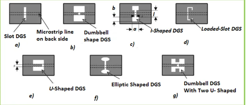
[image:37.595.113.525.406.639.2]Figure 2.11 shows several resonant structures that may be used [9]. The basic element of DGS is a resonant gap or slot in the ground surface (Figure 2.11a), placed directly under the transmission line and aligned for efficient coupling to the line. The dumbbell-shaped DGS (Figure 2.11b) includes two wide defected areas connected by a narrow slot. The conventional dumbbell-shaped DGS has been modified into an I-shaped DGS, as shown in Figure 2.11c. The frequency control of the I-shaped DGS is accomplished by adjusting the length of the transverse slot and the dimensions a and b. The stop-band
characteristic of the DGS in Figure 2.11c depends on l, which is the distance between
two rectangular lattices. In the U-shaped structure of Figure 2.11e, the loaded Q-factor increases as distance s decreases. Elliptic DGS cells are also obtained by etching a slot that connects two elliptic DGS shapes in a microstrip ground plane (Figure 2.11f). Figure 2.11g represents the DGS unit composed of two U-shaped slots connected by a transverse slot. This DGS section can provide cutoff frequency and attenuation pole without any periodicity, unlike other DGS [10].
2.9 Application of DGS
There are widely applications in active and passive devices useful for compact design. Since each DGS provides its own distinctive characteristics depending on the geometries, such circuit functionalities as filtering unwanted signals and tuning high-order harmonics can easily be accomplished by placing required DGS pattern, which correspond to the desired circuit operations without increasing circuit complexity [10].
2.9.1 Delay lines
Placements of DGS along a transmission line introduce changes in the propagation of the wave along the line. The DGS elements do not affect the odd mode transmission, but slows the even mode, which must propagate around the edges of the DGS “slot” [11].
2.9.2 Antennas
flat form factor is extremely attractive for transportable equipment or applications where a low-profile is essential.
Amplifier design also can benefit from DGS due to a number of attractive features that DGS have that can help to improve the amplifier performance. First, the DGS structure is very simple and it is easily simulated or fabricated and this is suitable for periodic structure design. Second, its stop band characteristic could be used to suppress certain harmonics.
There are various DGS studies in the literature not only for the analysis of the effect of the defects, but also for the implementation of the defects in various structures in microwave devices. It would be wise to have a look at the previous DGS studies first, and then present the contribution of this study.
Defected Ground Structure (DGS) is the first application that comes to mind when the line is preferably not disturbed. A defect on the ground can change the propagation properties of a transmission line with changing the current distribution on the ground side, and the alignment of the fields between the ground and the line.
The DGS studies conducted up to now have basically focused on the dumb-bell-shaped DGS which is basically proper for high frequency filtering applications [12-26]. The dumb-bell shaped defect is placed under the microstrip line as shown in Figure 2.13 Studies on the analysis of the structure have generally used the current density approaches to model the structure. The current density distribution is determined not only by the line path, but also by the discontinuities on the ground; and the resulting current distribution is interpreted as a physical model [27].
[image:41.595.98.505.495.684.2]Figure 2.13: Dumb-bell Shaped DGS.
The studies in the literature covered up to now are all of filter type or resonant type structures. However, non-resonant type applications of the DGS also exist. Rectangular-shaped defected ground structure (RS-DGS) resembles transmission line due to its physical structure. In this aspect, it can be claimed that a RS-DGS can be modeled as a
transmission line of characteristic impedance Zch not equal to the characteristic
impedance of the line with the same line width. This might be helpful if we need to increase the impedance to the levels where line widths cannot be realized easily.
Impedance matching at shorter distances is also realized by the use of the slow-wave characteristics of the DGS in the case of the space saving applications like amplifier input-output matching circuitries, hybrid couplers The usage of DGS at the input or the output of the amplifiers has also confirmed harmonic-rejection, and efficiency improvement properties [28-29].
2.9.4 Review of Previous Works
Hemant Kumar Gupta, P.K.Singhal, “Patch antennas designs with Defect Ground Structure in Efficient Rectenna Design for Wireless Power Transmission”. Rectenna is a rectified antenna means they are used for harvesting of microwave power, or convert Alternating Current (AC) power to Direct Current (DC) power. It is more efficient when antenna is design with more precision and accuracy like having lesser return loss and greater gain and directivity. To implement an efficient rectenna, design of microstrip
patch antenna with DGS is used. The work of the DGS structure is also proved that
harmonics are approximately removed by DGS Structure [30].
H.Takhedmit, B.Merabet, L.Cirio, B.Allard, F.Costa, C.Vollaire, O.Picon, “A 2.45-GHz Low Cost and Efficient Rectenna”. To improve the output DC power and decrease the required power densities, an antenna array must be developed and associated with the presented rectifier [31].
A. K. Arya, A. Patnaik, and M. V. Kartikeyan, “Microstrip Patch Antenna with Skew-F
REFERENCES
1. Constantine A. Balanis- Antenna Theory Analysis and Design, Second Edition, John Wiley & Sons,2001
2. David Sinchez-Hemindez and Ian D. Robertson, “Analysis and Design of a Dual-Band Circularly Polarized Microstrip Patch Antenna” IEEE Transactions on Antennas and Propagation, issue 43, No2, February, 1995.
3. Yogesh Kumar Gupta1, R. L. Yadava2, R. K. Yadav3, “Performance Analysis of 2.3 GHz Microstrip Square Antenna Using ADS, International Journal of Research in Management, Science & Technology, Vol. 1; No. 2, December 2013.
4. Peter Vaessen, “Wireless power transmission”, KEMA, September 2009.
5. Insik, C. and L. Bomson, “Design of defected ground structures for harmonic control of active microstrip antenna,” IEEE Antennas Propag. Soc. Int. Symp., Vol. 2, 852–855, 2002.
6. L. H. Weng, Y. C. Guo, X. W. Shi, and X. Q. Chen “An overview on Defect Ground Structure” in PIER VOl.7,173-189,2008.
7. T.-W. Yoo and K. Chang, "Theoretical and experimental development of 10 and 35 GHz rectennas," IEEE Trans. Microwave Theory Tech., vol. 40, pp. 1259-1266, June 1992.
8. Ramesh Garg, Prakash Bartia, Inder Bahl, Apisak Ittipiboon, ‘’Microstrip Antenna Design Handbook’’, 2001, pp 1-68, 253-316 Artech House Inc. Norwood, MA.
10.Ahn, D.; Park, J.-S.; Kim, C.-S.; Kim, J.; Qian, Y.; Itoh, T., "A design of the low pass filter using the novel microstrip defected ground structure," Microwave Theory and Techniques, IEEE Transactions on , Vol.49, no.1, pp.86-93, Jan 2001.
11.C. S. Kim, J. S. Park, D. Ahn, and J. B. Lim, “A novel 1-D periodic defected ground structure for planar circuits,” IEEE Microw. Wireless Compon. Lett., Vol. 10, no. 4, pp.131–133, Apr. 2000.
12.Liu, H., Z. Li, and X. Sun, “Compact defected ground structure in microstrip technology,”Electron. Lett., Vol. 41, No. 3, pp. 132–134, 2005.
13.Karmakar, N.C.; Roy, S.M.; Balbin, I., "Quasi-static modeling of defected ground structure," Microwave Theory and Techniques, IEEE Transactions on, Vol.54, no.5, pp.2160-2168, May 2006.
14.Ali Farahbakhsh, Mohammad Mosalanejad, “Using polygonal defect in ground structure to reduce mutual coupling in microstrip array antenna”, Journal of Electromagnetic Waves and Applications, Volume 28, Issue 2, pp: 194-201 2014.
15.Geng, Jun-Ping, Jiajing Li, Rong-Hong Jin, Sheng Ye, Xianling Liang, and Minzhu Li. "The development of curved microstrip antenna with defected ground structure." Progress in Electromagnetics Research 98 (2009): 53-73.
16.Gurpreet Singh,Rajni,Anupma Marwaha“Design of G-Shaped Defected Ground Structure for Bandwidth Enhancement”75, Issue 9, 2013.
17.Monopole Antenna Using Defected Ground Structure" IEEE Transactions on Antennas and Propagation, Vol. 59, no. 7, July 2011.
18.Yuchun Guo, Qing Wang “An Improved Parameters Extraction Method for Dumbbell-Shaped Defected Ground Structure” pp.197-200, 2010.
19.G. Xue, D. X. Qu, J. Li, et al., “Design of a novel DGS unit,” International Conference of Microwave and Milli- meter Wave Technology, pp. 354-356, 2008.
20.Arya, A. K. , Patnaik, A. and Kartikeyan, “Microstrip Patch Antenna with Skew-F Shaped DGS Skew-For Dual Band Operation”. Progress in Electromagnetics Research M, Vol. 19, 47-160, 2011.
22.L. H. Weng, Y. C. Guo, X. W. Shi, and X. Q. Chen“ An overview on defected ground structure” Progress In Electromagnetic Research B, Vol. 7, 173–189, 2008.
23.Amit Kumar Tripathi, B. K. Singh “A CPW Feed X-band Antenna for satellite and RADAR application” International Conference on Microwave and Photonics 2013.
24. Loveleen Cheema, Krishan Kumar Sherdia “Design of Microstrip Antenna with Defected Ground structure for UWB Applications” Vol. 2, Issue 7, July 2013. 25.Ashwini K. Arya, M. V. Kartikeyan, A .Patnaik, “Defected Ground Structure in
the perspective of Microstrip antenna,” Frequency, Vol.64, Issue5-6, pp.79-84, Oct 2010.
26.Sung, Y. J., C. A. Ahn, and Y. S. Kim, “Size reduction and harmonic suppression of rat-race hybrid coupler using defected ground structure,” IEEE Microwave and Wireless Components Letter, Vol. 14, No. 1, 7–9 Jun. 2004.
27.J. S. Lim, H. S. Kim, J. S. Park, D. Ahn, and S. Nam, “A power amplifier with efficiency improved using defected ground structure,” IEEE Microwave Wireless Compon. Lett., Vol. 11, pp. 170–172, Apr. 2001.
28.Vandana Chopra, Maninder Kaur, K.V.P Singh, Sumit Kumar Jha, “Design and optimization of microstrip patch antenna with defected ground structure and circular slot on the patch” International Journal of Research in Engineering Technology, issue 07, No2, July, 2013.
29.H.Takhedmit, B.Merabet, A 2.45-GHz Low Cost and Efficient Rectenna.
30.H. K. Gupta and P. K. Singhal “Patch Antennas Designs with Defect Ground Structure in Efficient Rectenna Design for Wireless Power Transmission” IJECCT 2012, Vol. 2 (4).
31.H.Takhedmit, B.Merabet, L.Cirio, B.Allard, F.Costa, C.Vollaire, O.Picon, “A 2.45-GHz Low Cost and Efficient Rectenna”.
32.A. K. Arya, A. Patnaik, and M. V. Kartikeyan, “Microstrip patch antenna with skew-F shaped DGS for dual band operation” Progress In Electromagnetics Research M, Vol. 19, 147-160, 2011.
34.Sanghamitra Dasgupta, Bhaskar Gupta and Hiranmoy Saha, “Development of Circular Microstrip Patch Antenna Array for Rectenna Application” IEEE INDICON 2010, Kolkata, INDIA December 17-19, 2010.
35.Liton Chandra Paul, Nahid Sultan, “Design, Simulation and Performance Analysis of a line feed Rectangular Microstrip Patch Antenna”, International Journal of Engineering Sciences & Emerging Technologies, Volume 4, Issue 2, pp: 117-126 Feb. 2013.
36.Kuldeep Kumar Singh, Dr. S.C. Gupta, “Design and Simulation of Microstrip patch array antenna for C Band Application at IMT (4400-4900 MHz) advanced spectrum with Series feed and parallel feed”, International Journal of Scientific & Engineering Research, Volume 4, Issue 12, December-2013.
37.S. Indrasen and T. V. S., "Micro strip Patch Antenna and its Applications: a Survey," International Journal of Computer Technology Application, vol. II, pp. 1595-1599, 2011.
38.M. T. Islam, M. N. Shakib, N. Misran and T. S. Sun, "Broadband Microstrip Patch Antenna," European Journal of Scientific Research, vol. 27, no. 2, pp. 174-180, 2009.
![Figure 2.6: Basic configuration rectangular patch with feed line [11]](https://thumb-us.123doks.com/thumbv2/123dok_us/8765537.896211/34.595.117.507.465.638/figure-basic-configuration-rectangular-patch-feed-line.webp)