Amadu Dainkeh
A thesis submitted in partial fulfilment of the
requirements of the University of East London for the
degree of Doctor of Philosophy
ii
ABSTRACT
The objective of this thesis is to investigate and provide better solution to producing filtered
power splitter with compact size and with use of no resistors for its isolation. The background
investigation and utilisation of the established theories build up the design equations that are
adapted to power dividers. These dividers contain filtering characteristics and are employed
in microstrip and substrate integrated waveguide technology.
The work involves the design of a filtered power splitter with bandpass characteristics. It
uses the conventional filter design synthesis to develop the design parameters that establish
the coupling between the common resonator of the power splitter and the next resonator
towards the output ports.
An equal and an unequal division using a 5-pole, 9-square resonators is used verify this
concept; this is also implemented in microstrip using Square open loop resonators (SOLR)
and in SIW. Furthermore, a 3-pole 5-square resonators is also implemented in SIW; all of
these operating at 2 GHz.
For the equal split, the 5th order microstrip gives a bandwidth, minimum insertion loss,
maximum return loss and isolation of 120MHz, 3.12dB, 15dB and 12.6dB respectively and
the 3rd order SIW gives a bandwidth, minimum insertion loss, maximum return and isolation
of 99Mhz, 3.57dB, 17.1dB and 6.79dB respectively; whilst the 5th order SIW gives a
bandwidth, minimum insertion loss, maximum return and isolation of 140Mhz, 3.87dB,
18.3dB and 14.79dB respectively. However, it is recommended that this work can be
extended to more than two output ports, to improve isolation, increase the Q factor and match
iii
I would like to express my gratitude to Allah for making it possible in my academic pursuit
this far. I would also want to give my particular thanks to my director of studies, Dr. Ken
Yeo for his supervision, guidance and encouragement all throughout my studies, since my
MSc. Thanks also go to Dr. W. Hosny for his advice and supports.
I would want to thank the staffs of the electronics lab at UEL, particularly Ben, for their
assistance, especially during my lab work.
Special thanks go to everyone who have supported in diverse ways through financial, advice
and encouragement. I really appreciate you all.
iv
TABLE OF CONTENTS
ABSTRACT ... i
ACKNOWLEDGEMENT ... iii
LIST OF FIGURES ... x
LIST OF TABLES ... xvi
ACRONYMS ... xvii
CHAPTER 1 INTRODUCTION ... 19
1.1 Thesis motivation ... 19
1.2 Research method ... 22
1.3 Aims and objectives ... 24
1.4 Thesis contribution ... 26
1.5 Thesis overview ... 27
CHAPTER 2 LITERATURE REVIEW ... 30
2.0 Introduction ... 30
2.1 Review of Microwave power divider ... 30
2.2 Review of substrate integrated waveguide ... 34
2.3 Applications substrate integrated waveguide to power divider ... 36
2.4 Summary ... 39
CHAPTER 3 POWER DIVIDER ... 40
v
3.2.1 N-way Power divider ... 45
3.2.1.1 Fork power divider ... 45
3.2.1.2 Tapered Power Divider ... 45
3.2.1.3 Radial Power divider ... 46
3.2.1.4 Sector-shaped power divider ... 46
3.2.2 Conventional T-Junction ... 48
3.2.3 Resistive Power Divider ... 51
3.2.4 Wilkinson Power Divider ... 53
3.3 S-matrix derivation of Wilkinson power divider ... 55
3.3.1 Even mode analysis ... 57
3.3.2 Odd mode excitation ... 59
3.4 Reflection and Insertion loss parameters ... 63
3.5 Polynomials of power divider ... 65
3.5.1 Two-port Power divider ... 65
3.5.2 Three-port Power divider polynomials ... 66
3.6 Summary ... 69
CHAPTER 4 COUPLED RESONATOR CIRCUIT ... 70
4.0 Introduction ... 70
vi
4.2.1 Electric Coupling ... 73
4.3.2 Magnetic Coupling ... 75
4.3.3 Determination of Coupling Coefficient ... 77
4.4 Determination of external quality factor ... 78
4.4.1 Single loaded Resonator ... 79
4.5 Determination of common resonators coupling coefficient factor ... 81
4.6 Summary ... 83
CHAPTER 5 FILTERED POWER SPLITTER USING SQUARE OPEN LOOP RESONATORS ... 84
5.0 Introduction ... 84
5.1 Overview ... 84
5.2 General Definition ... 85
5.3 Chebyshev Function Approximation ... 85
5.4 Lowpass Prototype Networks ... 87
5.5 Chebyshev Lowpass Prototype ... 89
5.6 Frequency and Element Transformations ... 89
5.6.1 Lowpass Transformation ... 90
5.6.2 Bandpass Transformation ... 91
5.7 Impedance Scaling ... 93
vii
5.9 5-pole Chebyshev’s bandpass filter circuit design ... 102
5.10 Power splitter circuit ... 106
5.11 Microstrip design of bandpass power splitter ... 109
5.12 Final Circuit Layout ... 112
5.13 Simulation and measured results ... 113
5.14 Design analysis ... 116
5.15 Summary ... 116
CHAPTER 6 ... 118
THEORY OF RECTANGULAR WAVEGUIDES AND SIW ... 118
6.0 Introduction ... 118
6.1 Overview ... 118
6.2 Rectangular waveguides... 119
6.3 Substrate Integrated Waveguide ... 122
6.4 SIW Cavity Parameters ... 123
6.5 SIW Effective width ... 125
6.6 Determination of the Microstrip parameters ... 126
6.7 Synthesis of w/h ... 128
6.8 SIW losses minimisation ... 128
viii
6.10.1 Coplanar waveguide (CPW)-to-SIW transition ... 131
6.11 SIW bandpass filter Design ... 132
6.12 SIW simulation ... 134
6.13 SIW Fabrication and measurement ... 140
6.14 Discussion ... 143
6.15 Summary ... 143
CHAPTER 7 ... 145
EQUAL AND UNEQUAL POWER SPLITTER IN SIW ... 145
7.1 Introduction ... 145
7.2 Determination of actual SIW resonator size ... 145
7.3 Coupling Coefficient extraction from SIW structure ... 147
7.4 External quality extraction from SIW structure ... 149
7.5 SIW power splitter implementation ... 150
7.6 Coplanar waveguide to SIW transition ... 157
7.7 Measurement Process ... 158
7.8 3-dB Equal power splitter ... 159
7.9 Fabrication and Measurement ... 164
7.10 3-pole unequal power splitter design ... 169
7.11 Fabrication and Measurement ... 172
ix
7.15 Fabrication and Measurement ... 185
7.16 Summary ... 188
CHAPTER 8 ... 190
CONCLUSION ... 190
REFERENCES ... 194
APPENDIX A Publications from this work... 207
x
LIST OF FIGURES
Figure 1.1 Divider cascaded with bandpass filter configuration (Tang and Mouthaan, 2010)
... 20
Figure 1.2 (a) two-port coupled resonator filter, (b) multi-port coupled resonator circuit (Skaik, 2011). ... 21
Figure 2.1 Phased array antenna system (Fenn et al., 2000) ... 31
Figure 2.2 Amplifier system schematic ... 32
Figure 3.1a Fork Power divider (Galani and Temple, 1977) ... 47
Figure 3.1b Tapered Power divider (Eccleston et al., 1997) ... 47
Figure 3.1c Radial Power divider (Fathy et al., 2006) ... 47
Figure 3.1d sector-shaped Power Divider (Abouzahra and Gupta, 1988) ... 47
Figure 3.2 T-Junction lossless transmission line model... 49
Figure 3.3 A Reciprocal, Lossless Three-Port Network Matched at Port 1 and 2 (Pozar, 2011) ... 51
Figure 3.4 Equal-Split Three-Port Resistive Power Divider ... 52
Figure 3.5 Equal-split Wilkinson power divider in microstrip form (Pozar, 2011) ... 54
Figure 3.6 Equivalent transmission line circuit (Pozar, 2011) ... 54
Figure 3.7 The Wilkinson power divider circuit in as normalized and symmetric form (Pozar, 2011) ... 56
Figure 3.8 (a) Even-mode excitation. (b) Odd-mode excitation (Pozar, 2011) ... 57
Figure 3.9 (a) Terminated Wilkinson Power Divider (b) Bisection Wilkinson Power Divider (Pozar, 2011) ... 60
Figure 3.10 Insertion loss S21 (dB) (Skaik, 2011) ... 65
xi
Lancaster, 2001) ... 73
Figure 4.3 An alternative form of the equivalent circuit with an admittance inverter j = ωCm to represent the coupling (Hong and Lancaster, 2001)………73
Figure 4.4 Synchronously tuned coupled resonator circuit with magnetic coupling (Hong and Lancaster, 2001) ... 75
Figure 4.5 An alternative form of the equivalent circuit with an admittance inverter 𝐾 = 𝜔𝐿𝑚 to represent the coupling(Hong and Lancaster, 2001) ... 76
Figure 4.6 input/output structure for SOLR coupled resonator circuit (Hong and Lancaster, 2001) ... 79
Figure 4.7 Input/output single loading equivalent circuit (Hong and Lancaster, 2001). ... 79
Figure 4.8 𝑆11 phase response of figure 3.7(Hong and Lancaster, 2001) ... 80
Figure 4.9 Split T power splitter model ... 82
Figure 5.1 Chebyshev filter response (Hong and Lancaster, 2001) ... 87
Figure 5.2 Lowpass prototype all-pole filters with: (a) a ladder network structure, and (b) its dual structure (Hong and Lancaster, 2001)………...87
Figure 5.3 Lowpass element transformation (Hong and Lancaster, 2001) ... 91
Figure 5.4 Bandpass element transformation (Hong and Lancaster, 2001) ... 92
Figure 5.5(a) Immittance inverters used to convert a shunt capacitance into an equivalent circuit with series inductance. (b) Immittance inverters used to convert a series inductance into an equivalent circuit with shunt capacitance (Hong and Lancaster, 2001): ... 94
xii
Figure 5.8 Bandpass networks using immittance inverters (Hong and Lancaster, 2001) .... 98
Figure 5.9 Generalized bandpass filter circuits using immittance inverters (Hong and Lancaster, 2001) ... 100
Figure 5.10 Bandpass Filter response (From MATLAB) ... 103
Figure 5.12 Making the Capacitors the same ... 104
Figure 5.13 Conversion to Band Pass Filter parameters ... 105
Figure 5.14 Circuit realization of the BPF ... 105
Figure 5.15 BPF frequency response of figure 4.14 ... 106
Figure 5.15 Coupling arrangement of a five-pole Chebyshev band-pass filtered splitter . 107 Figure 5.16 Equivalent circuit of a five - pole Chebyshev bandpass power splitter ... 108
Figure 5.17 Ideal circuit model responses for proposed five-pole Chebyshev filtered power splitter ... 109
Figure 5.18 Coupling Coefficient against spacing ... 111
Figure 5.19 External quality factor against tapping ... 112
Figure 5.20 Microstrip Schematic Layout of the 9 resonators power splitter ... 113
Figure 5.21 Simulated and measured responses of the fifth order filtering bandpass power filter. ... 114
Figure 5.22 Output ports return loss curves ... 115
Figure 5.23 Pictorial view of the 5-pole filtered power splitter ... 115
Figure 6.1. Substrate Integrated Waveguides (SIW) configuration (Deslandes and Wu, 2001) ... 119
Figure 6.2 Rectangular waveguide configuration ... 120
xiii
Figure 6.7 Electric Field Lines ... 127
Figure 6.8 MSL to SIW transition with tapered microstrip feeding: (a) transition structure; (b) electric field distribution in SIW cross section, and (c) electric field distribution in MSL cross section (Deslandes and Wu, 2001a), (Wu et al., 2003) ... 131
Figure 6.9 Configuration of the CPW-SIW transition (Deslandes and Ke, 2001) ... 132
Figure 6.10 Coupling coefficient of a pair of SIW cavities ... 136
Figure 6.11 Microstrip CPW to SIW input coupling structure for extracting 𝑄𝑒𝑥𝑡 ... 137
Figure 6.12 Graphs for extracting the external Q-factor, 𝑄𝑒𝑥𝑡 (a) Variation of 𝑄𝑒𝑥𝑡, with length, a, at constant length, b = 8.13 mm. (b) Variation of 𝑄𝑒𝑥𝑡, with length, b, at constant length, a = 0.7 mm ... 138
Figure 6.13 Substrate integrated waveguide bandpass filter layout with dimensions. ... 138
Figure 6.14 Simulation S-Parameter responses of the substrate integrated waveguide bandpass filter ... 139
Figure 6.15 Fabricated SIW bandpass filter pictures. (a) Top view. (b) Bottom view ... 140
Figure 7.1 Original rectangular shaped SIW resonator as captured from EmPro simulator ... 146
Figure 7.2 (a) Square shaped SIW resonator and (b) Simulated resonance frequency response ... 147
Figure 7.3 Two coupled SIW waveguide cavity resonators ... 148
Figure 7.4 |S21| of two coupled resonators showing two frequency peaks at 2GHz resonant frequency……….147
xiv
Figure 7.6 | | response curve depicting external coupling ... 150
Figure 7.7 Coupling Coefficients vs Spacing ... 151
Figure 7.8 Desired external quality factor determination ... 152
Figure 7.9 External Quality factor, Qe vs D3spacing ... 153
Figure 7.10 3-pole 5 resonators filtered power splitter topology ... 155
Figure 7.11 5-pole 9 resonators filtered power splitter topology ... 155
Figure 7.12 Simulation animation showing region of maximum electric field (in red) (a) 3-D view (b) Top view. ... 157
Figure 7.13 Microstrip line transition ... 157
Figure 7.14 Fabricated devices measurement set-up ... 158
Figure 7.15 Circuit schematic of the 3-pole Equal split filtered power splitter (ADS design) ... 160
Figure 7.15 (Continued) ... 160
Figure 7.16 Equal Power Splitter ideal circuit prototype response ... 161
Figure 7.17 (a) 3D structure (EMPro), (b) Top View of 3-dB equal split power divider .. 162
Figure 7.18 |S11|, |S21|, |S31| and |S23| EMPro simulation response of 3-pole equal split ... 163
Figure 7.19 Photograph of the 3-pole SIW equal division power splitter ... 164
Figure 7.20 Comparison of S11, S21 and S31 for Simulated and fabricated SIW power splitter ... 166
Figure 7.21 Equal split Simulated and measured S23... 167
Figure 7.22 Cross sectional top view of the power splitter ... 168
Figure 7.23 Circuit schematic of the unequal split filtered power splitter showing the lump elements L and C ... 170
xv
Figure 7.26 Photograph of the 3-pole SIW unequal division power splitter ... 172
Figure 7.27 Comparison of S11, S21 and S31 for simulated and fabricated 3-pole unequal division SIW power splitter ... 173
Figure 7.28 3-Pole unequal split simulated and measured S23 ... 174
Figure 7.29 EMPro 3D screen capture of the 5-pole SIW power splitter structure. ... 175
Figure 7.30 Circuit schematic of the 5-pole Equal split filtered power splitter ... 176
Figure 7.30 (Continued) ... 176
Figure 7.31 Equal Power Splitter ideal circuit prototype response ... 177
Figure 7.32 |S11|, |S21| & |S31| EMPro simulation response of 5-pole equal split ... 177
Figure 7.33 Photograph of the 5-pole SIW equal division power splitter ... 178
Figure 7.34 Comparison of S11, S21 and S31 for Simulated and fabricated 5-pole SIW power splitter ... 181
Figure 7.35 5-pole equal split simulated and measured S23 ... 182
Figure 7.36 Cross sectional top view of the 5-pole power splitter... 182
Figure 7.37 Circuit realization of the Equal split filtered power splitter ... 184
Figure 7.37 (Continued) ... 184
Figure 7.38 5-pole Unequal Power Splitter ideal circuit prototype response ... 185
Figure 7.39 Photograph of the 5-pole SIW unequal division power... 186
Figure 7.40 Comparison of S11, S21 and S31 for simulated and fabricated 5-pole unequal division SIW power splitter ... 187
xvi
LIST OF TABLES
Table 3.1 Merits and Demerits of three passive power dividers ... 63
Table 5.1 Design specifications ... 102
Table 5.2 Lumped element 𝒈 values ... 102
Table 5.3 Microstrip design specification ... 110
Table 5.4. Physical dimensions of the filtering splitter (mm) ... 113
Table 5.5. 5-pole FPS equal split Ideal, simulated and fabricated frequency responses comparison ... 117
Table 6.1 Test Bandpass design specifications: ... 133
Table 6.2 3-pole Chebyshev bandpass filter design parameters: ... 133
Table 6.3 SIW design parameters ... 135
Table 6.4 SIW Bandpass filter physical dimensions ... 139
Table 7.1. 2 GHz SIW resonator Parameters ... 154
Table 7.2 Power divider dimensions corresponding to the parameters in Figure 7.22 ... 168
Table 7.3 Common resonator coupling comparison (3-pole) ... 172
Table 7.4 Dimension comparison between designed and measured parameters ... 180
Table 7.4 (continued) ... 180
Table 7.5. Power divider dimensions corresponding to the parameters in Figure 7.36 ... 182
Table 7.6 Common resonator coupling comparison 5-pole ... 186
Table 7.7 Comparison of Ideal, simulated and fabricated SIW FPS’ frequency responses189 Table 7.7 (Continued) ... 189
xvii
ADS Advance Design system
BPF Bandpass Filter
BW Bandwidth
CBCPW Conductor backed coplanar waveguide
CPW Coplanar Waveguide
EBG Electromagnetic Bang Gap
EMI Electromagnetic Interference
EMPro Electromagnetic Professional
FBW Fractional Bandwidth
FEM Finite Element Method
FPS Filtered Power Splitter
FSIW Folded Substrate Integrated Waveguides
HMSIW Half-mode SIW
LTCC Low temperature Co-fired Ceramic
MCM Multichip Module
MMIC Monolithic Microwave Integrated Circuit
xviii
PCB Printed Circuit Board
PD Power divider
PS Power Splitter
Qext External Quality Factor
RWG Rectangular Waveguide
SIWs Substrate Integrated Waveguides
SOLR Square open loop resonators
TE Transverse Electrical
TEM Transverse Electromagnetic
TM Transverse Magnetic
UPS Unequal Power Splitter
19
INTRODUCTION
Recent development in the telecommunications industry has led to the success and
deployment of communications technologies including mobile and wireless communication.
There is extensive demand for new microwave and millimeter-wave components to cater for
the rapid growth in ultra-wide band system, broadband and wireless Internet, mobile and
personal communications, remote sensing and satellite navigation that have the capabilities
of meeting their stringent requirements. Filters, power dividers and diplexers are among the
components used in frequency selectivity and they play a crucial role in achieving these
systems realisations. There is a challenge in effective utilisation of the electromagnetic
spectrum, which possess the need to design and implement these components. The microstrip
antenna array feeding system needs a power divider with low loss, large bandwidth and high
Q-factor in order to enable high power handling. Power splitters are passive microwave
devices that are capable of splitting signal from the input port into at least two ports with the
signal of lesser power. To achieve this unit with such features, it is desired to implement a
component that is compact, lightweight and characteristics capable of usage in numerous
microwave applications.
1.1
Thesis motivation
Conventionally, bandpass filters power dividers are cascaded to be used in several
applications like image reject mixer and other circuits which produces two duplicated signals
20
(2005) and Llorente-Romano et al. (2003). Two identical bandpass filters are cascaded to a
power divider are shown in Figure 1.1 (Tang and Mouthaan, 2010). However, this
configuration requires a considerable area to be implemented. This thesis addresses a novel
network that can do the same functions of filtering and power splitting. Such networks are
based on coupled resonator structures and when compared to conventional configurations,
they may be miniaturized. The objective for the SIW power splitter design is to decrease the
overall dimensions, to be able to integrate with other passive components.
Figure 1.1 Divider cascaded with bandpass filter configuration (Tang and Mouthaan, 2010)
SIW-based components development symbolizes the revolutionary period in the design of
all microwave and mm-wave circuits. The use of the SIW technology in high performance
communication electronics is becoming very popular as integration density of electronics
components increases. It has been reported by some researchers that due to the high
Electromagnetic interference EMI isolation provided by the closed waveguide structures, the
SIW can eliminate the unwanted signals in sensitive microwave and mm-wave circuits. Also
some literatures including (Bozzi et al., 2008a) and (Kumari and Srivastava, 2013) have
demonstrated that low conductor losses and higher power handling in the SIW circuits
provide enhanced signaling performance when compared to other PCB based transmission
21
route signals in SIW-based systems, compact SIW power dividers are required. The designs
presented so far in literature follow the objectives of size reduction and achieving wide
operational bandwidth. In this thesis, the developed compact filtered power splitters will
provide a compact with even and uneven power splitting as well as filtering the signal as
required in many microwave systems. Figure 1.2 (a) gives an example of a two-port coupled
resonator filter topology. From the topology, the black dots depict resonators and the lines
linking the resonators are the couplings. Coupled resonator filters Synthesis methods have
been extensively presented in literatures. The work in this thesis implements the theory of
two-port coupled resonator filters and multi-port coupled resonator circuits as given in Figure
1.2 (b) with its main focus to three-port components such as coupled resonator power splitter.
The design approach allows the synthesis of filtering power dividers with arbitrary power
division
22
1.2
Research method
The most widely employed method when it comes to the design of RF and microwave filtered
Power dividers is a planar type which is based on lumped element equivalent circuit of
quarter-wave transformer (Jung-Hyun et al., 2002). This is having unique frequency, equal
magnitude and phase and with a three-port impedance matching network. The combining
network (i.e. the impedance matching network) is normally aimed at producing good
transmission and exhibiting high impedance in the passband, in order to achieve the
necessary output isolation (Wu et al., 2015).
The method of power divider design proposed in this thesis involves cascading two sections
of a single band bandpass filter with power divider as shown in Figure 1.1. Each bandpass
filter is designed with similar characteristics and frequency. The BPFs are connected in series
of lumped elements whose equivalent resonators are designed in microstrip and SIW`. The
main power division occur at the common resonator from the input port to the output channel.
The division can be equally or unequally done. Generally, Filters should have small insertion
loss, large return loss for good impedance matching with interconnecting components, and
high frequency-selectivity to prevent the interference and high performance. The electrical
performances of the filters are described in terms of insertion loss, return loss, and
frequency-selectivity (i.e., attenuation at rejection band) (Davidson, 2010). The parameters to consider
during this design include the operational bandwidth. This is the region of frequency at
passband that can allow signal to pass through. This crucial in any filter design as bandpass
mode is selected for a low interference environment (Cho and Rebeiz, 2014). Return loss,
measured in decibels (dB), is the loss of power in the signal returned/reflected by a
23
for all designs in this thesis is 20dB. Insertion loss, also measured in dB, is the loss of signal
power resulting from the transmission of these signals from the input ports to the output
channels in a transmission line. The magnitude of this loss is determined by the Q of the filter
circuit, usually supposed to be small (Dai et al., 2009); for example, in a 3dB power divider
the insertion loss might be specified as 0.5dB. Another parameter of importance
consideration in this design is Isolation. In an ideal power divider the output ports are
mutually isolated. In other words, a signal entering output 2 does not leak out of output 3.
Isolation is defined as the ratio of a signal entering output 1 that is measured at output 2,
assuming all ports are impedance matched (usually 50Ω ). Another parameter of importance
is the bandwidth, which is the frequency region that allows the signal to pass through.
To verify these concepts, the design equations are used to generate the values of the
parameters and its equivalent circuit model with lumped elements. A 5-pole microstrip equal
split FPS using SOLR is designed and tested. Then the SIW was adapted to a 3-pole and
5-pole equal and unequal split. This proposed FPS promise to give a design with compact size
while providing a low insertion loss and high return and isolation loss at 3GHz. The limit to
this frequency designed for is due to the available VNA network analyser of maximum 3GHz,
for the purpose of testing. The circuit model of the proposed FPS is simulated using the
Keysight Advanced Design System (ADS) circuit simulator, while the microstrip layout
simulation is achieved using the Keysight ADS momentum simulator. The electromagnetic
(EM) simulation of the SIW layout of the proposed filtered power divider is based on the
finite-element method (FEM) of the Keysight electromagnetic professional (EMPro) 3D
24
simulators could be used to achieve results similar to those presented in this thesis. The
microstrip filtered power divider’s fabrication is based on the printed circuit board (PCB)
milling process, while the SIW diplexer is fabricated using the PCB micro-milling process
based on the Leiterplatten-Kopierfrasen (LKPF) Protomat C60.
1.3
Aims and objectives
The aim of this research work is to develop compact filtered power divider with Chebyshev’s
bandpass performance for wireless applications using conventional, microstrip and substrate
integrated waveguide technologies.
The main objective is the design equations for even and uneven filtered power splitter and
the secondary objective is to implement it using microstrip and SIW technology.
The first objective of the project is to develop the design parameters for equal power splitter.
This achievement requires several approaches. The first approach is to develop filter design
variables using standard filter synthesis procedures. This also involves developing a
MATLAB code for determining the various parameters of the filter and the filter’s bandpass
response; determination of the coupling coefficients between resonators, and the external
quality factor at the ports of the filter. The second objective here is to develop the splitter’s
design parameters, especially for the coupling coefficient constant between the common
resonator and its next resonator; here the division ratio 𝛼 = 0.5 is the same for both output paths.
The second objective is to develop and design parameters for unequal power splitter. The
initial objective here is to develop the filter prototype parameters as done in the first aim. The
next objective is to develop filtered power splitter design parameters by implementing an
25
and 𝛼2 = 2/3, where 𝛼1 and 𝛼2 are division ratio towards port 2 and port 3 respectively. The third objective is to verify the first aim by implementing it in Microstrip and SIW. For
the microstrip, the first objective is to establish the relationships between parameters of the
model and behaviour of the Square Open Loop Resonators, SOLR, which requires the
development of a physical structure and employed in accordance with the design topology.
Next, bandpass SOLR filters should be designed according to the design procedure in order
to prove the viability of the presented model and procedure. The opportunities presented by
the developed theoretical model should be considered for this purpose. For the SIW, The first
objective is to determine the types of SIW resonators and potential coupling schemes, which
can be implemented in conventional rectangular waveguide, taking into account the
technological constraints. The second objective is to determine the type of microstrip-to-SIW
transition. Then a suitable design procedure should be determined for realization of SIW
bandpass filter. This should then be simulated and fabricated. The fabricated component
should then be measured to establish its filter response.
The fourth aim is to verify by implementing the second aim in SIW. The objective here is to
implement the unequal division power splitter in SIW technology. This should involve
manufacturing and testing of both power splitters for a third order 5 resonator and fifth order
9 resonator power splitter. The main objective is to create new SIW splitter with improved
performance using the approaches developed in this project from conventional rectangular
waveguides. A further objective is to study the available SIW filter and power divider design
and implementation techniques and find potential engineering solutions, which may improve
26
1.4
Thesis contribution
This thesis presents the readers with a comprehensive overview of the SIW research
conducted over the past decade. Following an in-depth analysis of the previously published
SIW research, an all-new 5 and 9 square resonator SIW-based components and systems are
developed in this thesis.
❖ The most important novelty is the comprehensive set of design equations to achieve even and uneven filtered powered filter. This is developed in Chapter 4 and applied
to the microstrip design in Chapter 5 and SIW design in Chapter 7.
❖ Another novelty is the design of microstrip filtered power splitter. A novel square open loop resonator (SOLR) power splitter is designed and reported in Chapter 5.
This topology and structure are designed using microstrip technology and its novelty
here is performance of filtering and splitting using this technology.
❖ Also, as a novel in this thesis is the implementation of the filter design and power splitter design concept of Chapter 4 and using the design parameters of the SIW in
Chapter 6 to the realise a physical structure of equal and unequal division power split
in SIW technology using square resonators; as reported in Chapter 7. The novelty is
the structure (SIW) and performance of the performing splitting and filtering signal.
The contribution of this thesis can also be attributed from these journals and conference
papers.
I. Dainkeh, A., Nwajana, A. O. and Yeo, K. S. K. (2016) 'Filtered Power Splitter Using
Square Open Loop Resonators', Progress In Electromagnetics Research C, 64, pp.
27
filter with new input/output connection'. 2016 16th Mediterranean Microwave
Symposium (MMS), 14-16 Nov. 2016, 1-4.
III. Nwajana, A. O., Dainkeh, A. and Yeo, K. S. K. (2017) 'Substrate Integrated
Waveguide (SIW) Bandpass Filter with Novel Microstrip-CPW-SIW Input
Coupling', Journal of Microwaves, Optoelectronics and Electromagnetic
Applications, 16(2).
1.5
Thesis overview
Chapter 1 introduces the brief background of the importance, characteristics and application
of power dividers in microwave technology. This chapter also explains the motivation to
embark on this project, the research method involved in executing these tasks and it gives the
aims and objectives, the contributions and overview of the thesis.
Chapter 2 gives the literature reviews of microwave power divider and substrate integrated
waveguide and their applications. Also included are summary of the evolution, benefits and
manufacturing techniques of these devices as given by numerous researchers. Some of the
gaps that led to this research are also identified and reported.
Chapter 3 provides the reader with a comprehensive background of microwave power divider
including its types and application found in literatures. The chapter also presents the theories
and mathematical modeling associated with power dividers including Scattering matrix and
28
basis to the synthesis of three-port components such as power splitters in chapter 5 and
chapter 7.
Chapter 4 presents an introduction the theory coupled resonator circuits. This chapter
develops various mathematical expressions, including generating expressions for the
coupling coefficients between resonators and external quality factor for filter and PS design.
Also, it provides the coupling expression between the common resonator to the output ports
and the next resonator along that path for the PS. The evaluation of this chapter is vital for
its adoption to Chapter 5, Chapter 6 and Chapter 7. Also included are the design expressions
for the microstrip design.
Chapter 5 focuses on SOLR power splitter components in microstrip technology. The
findings of chapter 3 and chapter 4 are used to realise this power splitter. A review of
standard microstrip theory and technology is included; and adapted to the design of the SOLR
microstrip line technology. This is followed by simulation and optimisation. This chapter
also includes fabrication and measurement evaluations of the filtered SOLR power splitter.
Substrate integrated waveguide cavity resonators is presented in Chapter 5.
Firstly, it utilizes Maxwell’s equation and conditions to formulate expressions relating to
rectangular waveguides. Theories and mathematical modeling derived from the previous
section will be analysed. This includes, SIW supported propagation mode and expressions to
29
bandpass filter. This chapter specifically deals with the novel coplanar to SIW transition at
both input and output ports of an SIW bandpass filter. The coupling coefficient and Q factor
are determined and it explains the SIW design process and simulations carried out in order
to ascertain the correct dimensions. It also highlighted the SIW design process and the output
frequency response curve after testing and the tuning process used to improve the result.
Chapter 7 presents coupled resonator power splitters that are designed and realised using
SIW resonators to verify the new design methodology. The designed components are as
follows: (1) Third-order equal division power splitter. (2) Third-order unequal division power
splitter. (3) Fifth-order equal division power splitter and (4) Fifth-order unequal division
power splitter.
Lastly, Chapter 8 provides summary and conclusions drawn from this thesis. Future work
30
CHAPTER 2
LITERATURE REVIEW
2.0 Introduction
This chapter gives a review of many literatures as applied to power dividers and SIW and
their applications. It includes the problem domain and what the existing research gaps are
and how they have been addressed. It also discusses some of the limitations of the existing
state of the art solution and lastly how this thesis intends to solve some these problems.
2.1 Review of Microwave power divider
A power splitter is a module that is frequently used in telecommunication and radar. The idea
of power splitter dates back to 1940 when a variety of power dividers and couplers were
invented at the MIT Radiation Laboratory (Fenn et al., 2000, Hong and Lancaster, 2001).
Among them were the E & H plane waveguide T-junction, multi-hole coupler and different
types of couplers using coaxial probes. Between 1950 & 1960 many of these Power dividers
were re-invented with strip-line and microstrip technology. It was mainly due to increase in
planar line usage and led to the development of Wilkinson Power divider and branch line
couple (Pozar, 2011). The recent development of telecommunication equipment has shown
a tendency to produce modules with unique splitting features.
In many microwave applications, power dividers/splitters have been used widely. Various
examples include combiner network for solid-state power amplifier and applications in
31
equal division; alternatively, it can also be fed to a splitter arranged in a series of equal split
power dividers. These divided signals are then transferred to a transmitting antenna through
phase shifters. These antennas are used in beam steering applications that need direction
[image:31.612.178.484.192.395.2]change of the antenna beam with time.
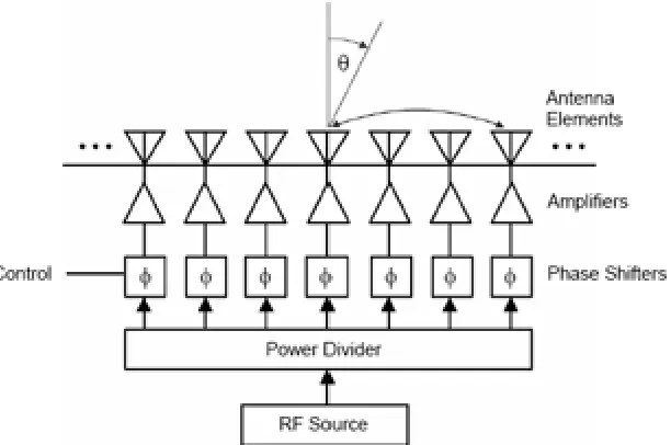
Figure 2.1 Phased array antenna system (Fenn et al., 2000)
Figure 2.1 shows a phase array antenna system that consists of phase shifters, amplifiers and
antenna element (Ehmouda, 2009). These microwave devices use passive components for
splitting or combining. In power splitting, an input signal is divided into two or more signals
with lesser Power. The divider Power can be equal division or unequal division depending
on the purpose for which it is designed. Three ports network are the simplest form of power
dividers. To form a multi-stage structure, an extension of using N-way power splitters are
used.
Commonly used power dividers in microwave system and circuits are the T-junction (Pozar,
2011) and the Wilkinson (Wilkinson, 1960) power dividers. Also, directional couplers and
32
ports, It contains a phase shift of either 180o (Magic-T) or 90o (branch-line hybrids) (Pozar,
2011).
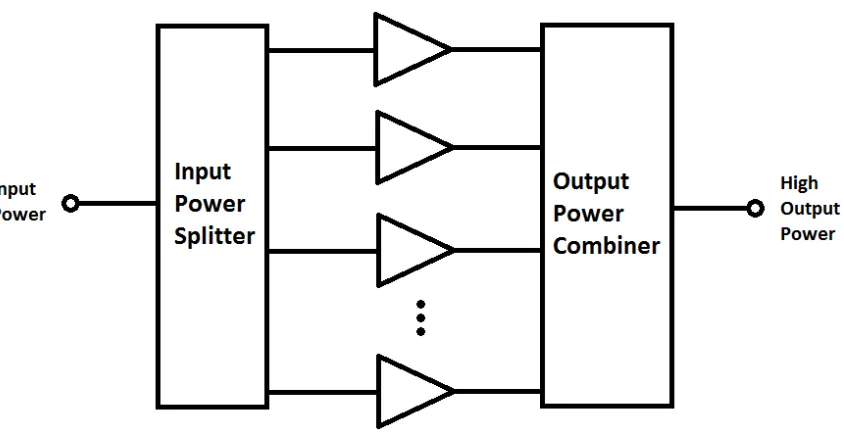
Power divider or combiner network circuits are used when high power is required, as in case
of distributed power amplifier system (Pengcheng et al., 2003) as shown in Figure 2.2. There
is a combination of output power from a large number of power amplifiers. The power splitter
first divides the power, which gives the power amplifiers a drive signal. The output of the
amplifier then combines to form a single output with huge power by the use of the power
combiner. Usually, the networks required for power division or combination needs to have a
high port isolation and low loss in these systems. Tianyu and Wenquan (Zhang and Che,
2016) have designed a miniaturised network that promises to be use in this applications,
however, the issue of a lossless network couldn’t be achieved due to resistor component in
[image:32.612.126.548.414.635.2]the output isolation.
Figure 2.2 Amplifier system schematic
33
1995). Such filters have reflection and low losses performance characteristics, which is
compatible with optical single mode fibers. It uniformly distributed the output power on the
N-way waveguide. This proposed method avoided the sharp edges that are near to the
branching point thus led to a process-tolerant design. Its structure is produced in
fiber-compatible integrated devices due to it is inherent in the silica-on-silicon technology.
There have been many designs of power splitters. Recently, multi-layer microstrip
technology has been used. This is used for the reduction of size of the microwave
components. They are designed using different design methodologies and geometries, for
example, a power splitter (PS) based on multilayer slot-line technique with bandpass filtering
(Song and Xue, 2010), (Abbosh, 2007), (Abbosh and Bialkowski, 2007). Even though they
are shown to give good insertion loss performance they are, however, complicated to
fabricate due to exact positioning of the orthogonal isolation resistance (Song and Xue,
2010). In (Abbosh, 2007), a 3-way PS based on multilayer broadside coupled structure was
presented. It shows a good power division and isolation but it’s difficult to align and fabricate
due to the two ground planes that the structure needs (Abbosh and Bialkowski, 2007).
In (Chen et al., 2013), miniaturized power divider with band-pass characteristics based on
coupled-resonator topology was presented, the reduced circuit are due to shrinking of
assembled resonator. A general unequal two way power splitter was designed by (Parad and
Moynihan, 1965) and some design equations for a multi-way unequal power splitter and the
design method for multi-way dual band, due to the development of dual band PS, is seen in
(Hee-Ran et al., 2004) and (Wu et al., 2010) respectively. But they all failed to miniaturise
34
focused on miniaturising the PS. The isolation impedance is placed within the quarter
wavelength of the transmission line to be used for interconnection and impedance
transformation to make the structure avoid extra line. However, the PS electrical length was
not reduced (Wang et al., 2014), (Trantanella, 2010), (Choe and Jeong, 2014). There has been
reduction of the electrical length and characteristics impedance for a four-way equal PS, but
this cannot be used for UPS.
2.2
Review of substrate integrated waveguide
In the past few decades, there has been remarkable amount of research carried out to develop
high-performance millimeter-wave and microwave waveguide components that are
manufactured using low-cost technologies. Substrate integrated waveguides (SIWs) are
among these. It was introduced initially as laminated waveguides (Hirokawa and Ando,
1998) and (Uchimura et al., 1998) that can be implemented easily using printed circuit board
(PCB) technology of fabrication. Since SIWs and laminated waveguides are introduced,
numerous SIW-based components, circuits and interconnects have been developed and their
advantages are justified when compared to waveguide or equivalent transmission line based.
It has been discovered that Q factor and power handling achieved with SIW resonators are
much higher than what’s attained with traditional planar microstrip or stripline results, which
made the SIW cavities the best entity for application in direct and cross-coupled filters (Bozzi
et al., 2009b). However, the physical dimensions of SIW circuits may be too large for certain
applications, especially those operating at low frequencies. Among the approaches to achieve
reduced size of SIW resonators and filters there are ridged SIW (Shelkovnikov and Budimir,
35
(FSIW) structures, which not only reduce the area occupied by waveguides or resonators on
a chip but also offer new design solutions to realize advanced cross-coupled filters with and
without non-resonating nodes (NRN). Hong (Hong, 2006) proposed and compared two types
of compact FSIW resonant cavities. A quarter-wavelength FSIW cavity, obtained by the
successive folding of a conventional 𝜆 2⁄ wavelength FSIW resonator, has been successfully developed, employed and implemented on a cross-coupled filter (Alotaibi and Hong, 2008);
another miniaturisation method for FSIW resonators has been established in (Lin, 2007); a
directional filter built upon a half-mode SIW (HMSIW) has been proposed in (Wang et al.,
2007).
Substrate integrated waveguide (SIW) interconnects provide a broadband bandpass signaling
medium with excellent electromagnetic interference (EMI) isolation (Suntives and Abhari,
2007), while planar conventional transmission lines are known as the performance tailback
in ultra-wideband systems due to their high-frequency losses and limited bandwidth. The
electric field in an SIW distribution fills the volume inside the waveguide interconnect and
surface currents propagate on the larger total cross-sectional area of the waveguide walls,
thereby reducing conductor losses (Patrovsky et al., 2007). Due to the open structure and
increased susceptibility to EMI and unwanted signal transfer, closely spaced stripline and
microstrip will no longer be a good option system module interconnection.
There has been continuously increasing demand for compact electronic systems and
wideband interconnects. This brought about the necessity of using SIW technology in future
UHF, broadband and highly integrated systems application.
36
with other planar circuits and other lines. However, this may be challenging and many
researchers have developed different modes of impedance matching transition from stripline,
microstrip, coplanar waveguide and conductor backed coplanar waveguide (CBCPW) to
SIW (Deslandes and Wu, 2001), (Rayas-Sanchez, 2009). Just like the SIW, these transitions
are all implemented using the same process of fabrication just like the rest of the system’s
layout.
2.3
Applications substrate integrated waveguide to power
divider
Components such as filters, Power Dividers and resonator cavities have now been
redeveloped to SIW based platform. One of the most criticised about SIW components is its
large size, However, research that has been published by (Grigoropoulos et al., 2005) and
other researchers like (Izqueirdo et al., 2006) and (Che et al., 2008) have particularly focused
in trying to miniaturise these components.
Numerous types of SIW diplexers, couplers and power dividers have been implemented and
optimised for operation at millimeter and microwave frequency bands using PCB substrates
as explained by several researchers including (Zhen-Yu and Ke, 2008) and (Shen et al.,
2009). Other SIW-based components like waveguide cavities have also been directly
integrated into a PCB platform, thus, allowing significant cost decrease in the development
and mass production of resonator-based microwave components including filters and
oscillators. The waveguide cavities high quality factor provides excellent frequency
selectivity for cavity coupled resonators (Hill et al., 2001).
37
Nowadays, it’s possible to develop a fully integrated multichip module (MCM) systems
incorporating high-gain antennas and SIW filters. SIW cavity-backed antennas and slot array
SIW antennas enables microwave designers to incorporate low cost, high-performance
antennas on the same substrate as monolithic microwave integrated circuits (MMIC)(Ocket
et al., 2009)
There is huge interest in space exploration, including mission to Mars and SIW technology
is one of the most attractive design platforms. Reducing payload is critical in maximising
fuel efficiency as a result of the very long astronomical travel distances of such missions.
Ultra-light SIW-based electronic communication systems development will reduce the
overall spacecraft and satellite payloads when compared to the units deployed with milled
metallic waveguides (Daneshmand and Mansour, 2005). Lightweight SIW antenna arrays are
critical in the development of portable communication base stations for space exploration
systems. Also, SIW components are excellent choice for Earth orbiting satellites,
ground-to-air base stations and un-manned drone ground-to-aircraft applications as well as high-speed data hubs
and Internet.
In comparison to other popular planer guiding structures like microstrip and CPW, SIW
offers lower losses (Khan et al., 2013) but occupies larger area. Therefore, miniaturisation of
SIW based components is essential for a compact design. The width of a half-mode SIW
(HMSIW) is almost half of that of a standard SIW (Jones and Daneshmand, 2016). So,
components based on HMSIW occupy smaller area. Using the HMSIW technology, a
compact four-way equal split power divider is reported in (Zou et al., 2011). In (Jin et al.,
38
(QMSIW). In (Zhang et al., 2015), further miniaturisation is obtained by one-eighth mode
SIW resonator (EMSIW). EMSIW is utilised to design compact bandpass filter. In all the
components, SIW-to-microstrip transitions are used for SMA connection. On the other hand,
to reduce the circuit size and the loss introduced by SIW-microstrip transition, direct coaxial
feed is used in SIW power dividers. In (Seo et al., 2009), a coaxial feed at the center of a
rectangular SIW structure is used as the input and SIW-to-microstrip transitions are used for
the output ports. Further, metallic posts are used to control the output power levels at the
output ports. Whereas in (Song et al., 2008), equal split eight-way power divider using direct
coaxial feed at all the ports is reported. Size reduction is achieved but suffer low bandwidths
of the power dividers.
Studies on SIW based equal power dividers are described in (ZhargCheng et al., 2005),
(Tiwari et al., 2015). In (Datta et al., 2013), (Karimabadi and Attari, 2012) , studies on
broadband equal power divider using SIW technology are presented. Design of an equal and
unequal power divider is described in (Yang and Fathy, 2007) but suffers mismatch between
the predicted and measured insertion and also failed to include the output isolation.
In this thesis, a simple design approach is described to implement SIW based equal and
unequal power divider while maintaining a broad operating bandwidth and capable of not
transferring signals between the output ports. The manufactured component promises to be
39
This chapter has presented a brief literature review of some existing literatures relating to PD
and SIW, it has highlighted some of the problems with these designs and what needed to be
done in order to improve these gaps. Some of these gaps have been address and are also
indicated. It has also shown the reasons that prompted this research through attempting to
Chapter 3 –Power Divider
40
CHAPTER 3
POWER DIVIDER
3.0 Introduction
In this chapter, emphasis will be made to theories relative to power dividers. It will outline
the various examples of PD including some of their advantages and their respective
applications and topologies as being used microstrip technology. The scattering (S) matrix is
presented in which its phenomenon is used to express the insertion loss, return loss, isolation
etc. of the PD. It provides the matrix from the theory of incident and reflected wave. The
next section outlines the various types of PD that led to the development of the PD concept,
including the Wilkinson PD. The following section focuses on the S-parameters of the
Wilkinson PS owing to its unique PD characteristics. Then the reflection and insertion loss
parameters are discussed using its mathematical expressions and lastly it outlines a brief on
the PD polynomials.
3.1 Scattering matrix
The scattering matrix is used to express the characteristics of a power divider. It is also known
as the S-matrix and it is used to give the relationship between voltage waves that are incident
on a device port with respect to the voltages, which are reflected on the device port,
considering both phase and magnitude. Equation 3.1 gives the S-matrix in terms of its
41
[ 𝑉1 𝑉2−
⋮ 𝑉𝑁−
] = [ 11 𝑆21 12 𝑆22 1𝑁
⋯ 𝑆2𝑁
⋮ 𝑆𝑁1
⋮ 𝑆𝑁2
𝑆33 ⋮
⋯ 𝑆𝑁𝑁
] [
𝑉1 𝑉2+
⋮ 𝑉𝑁+]
(3.1)
This equation can as well be written as:
[𝑉−] = [𝑆][𝑉+] (3.2)
From the above equations, the appropriate incident and reflected voltage wave can be used
to deduce each S-matrix element. Therefore, the general equation for the S-matrix element
can be defined as:
𝑆𝑖𝑗 = 𝑉𝑖−
𝑉𝑗+|𝑉
𝑘+=0 𝑓𝑜𝑟 𝑘≠𝑗
(3.3)
This equation implies that the ratio of the reflected wave of the voltage 𝑉𝑗+ to the incident wave of the voltage 𝑉𝑖− gives the element of the S-matrix 𝑆𝑖𝑗; where the incident wave is the
driving port 𝑗 and port 𝑖 exits the reflected wave. In addition, the incident waves on all ports are set to zero except the 𝑗𝑡ℎ port. This implies that to avoid reflections, all ports should be terminated in matched load. This can be used to explain that when looking at port 𝑖, 𝑆𝑖𝑖is the reflection coefficient and 𝑆𝑖𝑗 is the transmission coefficient from port 𝑗 to port 𝑖 when all other ports have been terminted in matched loads (Pozar, 2011). To measure these
parameters, a Vector Network Analyzer (VNA) is typically used. For power divider, which
contains three ports, any port that is not measured is terminated with a matched load.
The input impedance as seen at each port is equivalent to the system's characteristics
impedance when all the ports are matched. The reflection coefficient of the equivalent
Chapter 3 –Power Divider
42
Therefore, the reflected wave voltage at that reference point is zero. Since the reflected wave
is zero, from equation e.3 (the S-matrix element where 𝑖 = 𝑗 ), it is obvious that the S-matrix element is also zero. This, therefore, shows that when a device is properly matched at each
of its port, the S-matrix diagonal element will all be zero (Pozar, 2011, Grebennikov, 2011).
Power dividers, like other devices, possess a common characteristic, which is reciprocity.
Reciprocity is a concept used to describe the power-transmitted devices or network ports
similar irrespective of the propagation direction through the device or network. Hence for a
reciprocal network;
𝑆𝑖𝑗 = 𝑆𝑗𝑖 (3.4)
For all values of 𝑖 and 𝑗. This relationship shows that the reciprocal network has a symmetrical S- matrix (Pozar, 2011).
Another unique feature of the S-matrix is the amount of power which is lost that is attributed
to it network. It would have been ideal for a power divider that is lossless to have been used,
however, a completely lossless power divider is physically unrealisable. It has been
highlighted on several occasions by (Pozar, 2011) that for a lossless network, the S-matrix
must be unitary.
[𝑆]𝑡[𝑆]∗ = [𝐼] (3.5)
Where the 𝑡 represents the matrix transpose, the asterisk represents the matrix conjugate and 𝐼 is the identity matrix. A unitary matrix means that the sum of squares of the column elements
43
Critical to the performance of output port of a power divider is the isolation. Isolation is a
characteristic that possesses the ability to isolate signal between ports or for signals from one
output port not to affect the other output port. For power divider, three port device, which
has two outputs, 2 and 3. It is vital to reduce the unwanted signal transfer caused by the
coupling between the ports. The element 𝑆23 and 𝑆32 are used to represent the isolation between the output ports 2 and 3. The 𝑆23 represents the signal leaving the port 2 and entering the port 3 and 𝑆32, the reverse. A high isolation is achieved between port 2 and 3 when the magnitude of these elements are small (Pozar, 2011, Grebennikov, 2011, Chang, 2005)
An ideal power divider will be a very low loss or lossless, matched at each port and be
reciprocal. However, this is impossible to achieve. To demonstrate that any three-port power
divider network exhibits the ideal characteristics. Consider the S-matrix:
[𝑆] = [
𝑆11 𝑆12 𝑆13
𝑆21 𝑆22 𝑆23
𝑆31 𝑆32 𝑆33
] (3.6)
Firstly, it is assumed that the device is reciprocal and matched to all the ports. Based on the
relationship for the reciprocal and matched port cases, applying them to the S-matrix reduces
the generic three-port S-matrix to (Collin, 2001):
[𝑆] = [
0 𝑆12 𝑆13
𝑆12 0 𝑆23
𝑆13 𝑆23 0
] (3.7)
As stated above, for lossless condition, the sum of squares of column elements of the
S-matrix in equation 3.7 must be unitary; that is equal to 1.
|𝑆12|2+ |𝑆
Chapter 3 –Power Divider
44
|𝑆12|2+ |𝑆
23|2 = 1 (3.8b)
|𝑆13|2+ |𝑆23|2 = 1 (3.8c)
𝑆∗13𝑆23= 0 (3.8d)
𝑆∗23𝑆12= 0 (3.8e)
𝑆∗
12𝑆13= 0 (3.8f)
This means that two of the three elements, 𝑆12, 𝑆13, and 𝑆23 must be zero in order to satisfy (equations (3.8a – 3.8f). For analysis purpose, 𝑆12 and 𝑆13 are set to zero. However, by setting these parameters zero equation 3.8a is not achieved as the sum gives zero. Consequently,
when any two of the three 𝑆12, 𝑆13, and 𝑆23 are zero, then one of the equations 3.8a -3.8b will not be fulfilled. This therefore makes matched ports, lossless and reciprocal three-port
network impossible to obtain (Pozar, 2011, Grebennikov, 2011, Chang, 2005).
3.2 Types of power divider
Although the ideal characteristics including reciprocal, matched and lossless of a power
divider, are not physically realisable, there are some power dividers that exhibit at least two
of the idle properties. The common power dividers with its unique features are T-Junction,
resistive and the Wilkinson power divider. One of the various methods that is used to
construct power divider is transmission lines method. This include, using a microstrip or
45
3.2.1 N-way Power divider
The N-way power splitter is used extensively in microwave applications, especially where it
is required to split and then combine microwave power. Due to ease of manufacturing and
low cost, microstrip line technology is mostly used in this N-way power divider and this can
be easily integrated with amplifier system. There are several common N-way microstrip
power divider; they include Fork power divider (Galani and Temple, 1977), radial power
dividers (Fathy et al., 2006), tapered line power dividers (Yau et al., 1986) and sector-shaped
power divider (Abouzahra and Gupta, 1988). Shown in Figure 3.2(a-d) are examples of the
various power dividers discussed.
3.2.1.1 Fork power divider
The Fork power divider has low loss characteristics, a broad bandwidth and between its
output ports, there is a good isolation performance (Galani and Temple, 1977). The divided
part consists of N number of transmission lines as shown in Figure 3.1a. The adjacent output
ports contain an N-1 number of isolation resistors and a quarter wavelength at the center
frequency with input characteristics impedance Z0.
3.2.1.2 Tapered Power Divider
The tapered microstrip power divider is advantageous as it provides a good amplitude, phase
Chapter 3 –Power Divider
46
microstrip line power divider are located in a straight line and the function of the holes the
module is to ensure that there is equal transmission path length from input to the output port
(Eccleston et al., 1997).
3.2.1.3 Radial Power divider
The radial Power divider is popular in its ability in achieving an N-way power division. It
presents an excellent phase and amplitude performance balance and low noise, particularly
for higher N (Fathy et al., 2006). There is two sections which the Radial Power splitter
consists of: the radial line and the launcher. The radial line is used to divide the signal into
the output ports that are positioned around the edge of the radial line. It's made of parallel
plates transmission lines with low loss and has a circular shape. The launcher section is the
coaxial line that serves as a feed to the radial line in the middle. An example of radial power
divider is shown in Figure 3.1c.
3.2.1.4 Sector-shaped power divider
The sector-shaped power divider also contains a good balance performance of phase and
amplitude and wide bandwidth. As seen in the example of Figure 3.1d (Abouzahra and Gupta,
1988), this power divider uses a sectoral transmission line to split the signal into the various
N output ports. These ports are equally spaced and positioned on the sectorial side.
The radial power divider is a non-planar structure since it requires a probe (vertical) coaxial
line feeding port, whilst the other three power dividers, which are Fork, tapered and
47
(a) (b)
[image:47.612.128.528.95.477.2](c) (d)
Figure 3.1a Fork Power divider (Galani and Temple, 1977) Figure 3.1b Tapered Power divider (Eccleston et al., 1997)
Figure 3.1c Radial Power divider (Fathy et al., 2006)
Figure 3.1d sector-shaped Power Divider (Abouzahra and Gupta, 1988)
In summary, it is generally required that to achieve an improved isolation performance, the
isolation resistors which are located between the output ports can be used and an N-way
power divider requires a very good isolation over its bandwidth (Fathy et al., 2006,
Chapter 3 –Power Divider
48
When high power output is required in any power amplification system, power
dividing/combining networks are essential (Zhang et al., 2010), (Yam and Cheung, 1997)
and (Pengcheng et al., 2003). The input power divided firstly by the power divider to provide
the signal that can be supplied to the power amplifiers. Using the power combiner, these
amplified output signals can be combined into a single output with a higher power. Figure
2.2 shows an example of this system where there is a combination of output power from the
many power amplifiers. There is structural identity between the N-way power divider and
power combiner except that their inputs and output are placed in opposite order. When the
power divider/combiner is symmetrical, the signals which are combined from the power
amplifier should be the same in phase and magnitude to a maximum combining efficiency
(Gupta, 1992).
3.2.2 Conventional T-Junction
The conventional T-Junction power divider is lossless which contains three transmission
lines all connected at its common junction. There is a reactance linked to this junction. This
is due to the effect of the fringing field and higher order mode. The T-Junction lossless
49
Figure 3.2 T-Junction lossless transmission line model
Even though this power divider is lossless, it suffers a drawback that not all the ports are
matched and there is no isolation between its output ports. Lumped susceptance B can be
used to represent the stored energy. To match the input characteristics 𝑍0, equation 3.9 must be satisfied:
𝑌𝑖𝑛 = 1
𝑍0 = 𝑗𝐵 +
1 𝑍1+
1
𝑍2 (3.9)
For a lossless or very low loss transmission lines, it means the characteristics impedances are
real, that is the imaginary component is zero, and this makes 𝐵 = 0. This equation 3.9 now becomes:
1 𝑍0=
1 𝑍1+
1
𝑍2 (3.10)
Some reactive tuning elements can be utilized in the power divider configuration if B is not
Chapter 3 –Power Divider
50
Various power division ratios can be generated by calculating the output line impedance 𝑍1 and 𝑍2. For example, for an equal split (3dB) power divider, it can be designed by using two 100Ω for an input transmission line impedance of 50Ω. A quarter wavelength transformer
could be utilised to realise the output lines impedance to its desired values. The input lines
impedance are matched when the output lines are matched, however, the output ports will
have no isolation.
If only two ports are matched, say port 1 and port 2, then a three-port network can be realized
which is reciprocal and lossless. Hence, the scattered matrix is thus:
[𝑆] = [
0 𝑆12 𝑆13
𝑆12 0 𝑆23
𝑆13 𝑆23 𝑆33
] (3.11)
Again, the following unitary conditions are achieved to make it lossless:
|𝑆12|2+ |𝑆13|2 = 1 (3.12a)
|𝑆12|2+ |𝑆23|2= 1 (3.12b)
|𝑆13|2+ |𝑆23|2+ |𝑆33|2 = 1 (3.12c)
𝑆∗
13𝑆23 = 0 (3.12d)
𝑆∗12𝑆13+ 𝑆∗23𝑆33 = 0 (3.12e)
𝑆∗23𝑆12+ 𝑆∗33𝑆13 = 0 (3.12f)
Equation 2.12a and equation 2.12f gives that |𝑆13| = |𝑆23|. This solves equation 3.12d to be
51
lines and a mismatched one-port. The matrix and signal flow diagram for this arrangement is
given below (Pozar, 2011).
[𝑆] = [ 0 𝑒
𝑗𝜃 0
𝑒𝑗𝜃 0 0
0 0 𝑒𝑗𝜃
[image:51.612.170.501.140.428.2]] (3.13)
Figure 3.3 A Reciprocal, Lossless Three-Port Network Matched at Port 1 and 2 (Pozar, 2011)
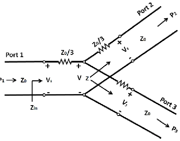
3.2.3 Resistive Power Divider
For all the output ports to all be matched, a lossy component is introduced to the three-port
network. However, there is no isolation between the output ports. This type of power divider
52
Figure 3.4 Equal-Split Three-Port Resistive Power Divider
Standard circuit theory can be used to analyze the resistive power divider. The characteristics
impedance Zo is used to terminate all the ports. Equation 3.14 gives the combination of the
output lines and the impedance of 𝑍0/3 resistor.
𝑍 =𝑍0
3 + 𝑍0 = 4𝑍0
3 (3.14)
The input impedance Zin of the divider is given by:
𝑍𝑖𝑛 =𝑍0
3 + 2𝑍0
3 = 𝑍0 (3.15)
All of the ports are matched since the resistive PD is symmetrical as demonstrated by
equation 3.16.
53
Assuming that the voltage at the input port one is V1, the voltage at the junction connecting
all the ports is:
𝑉 = 𝑉1 2𝑍0⁄3
𝑍0⁄ +2𝑍3 0⁄3=
2
3𝑉1 (3.17)
The output voltages are then calculated as:
𝑉2 = 𝑉3 = 𝑉 𝑍0
𝑍0+𝑍0⁄3=
3 4𝑉 =
1
2𝑉1 (3.18)
This makes 𝑆21= 𝑆31 = 𝑆23= 1/2. Since the resistive power divider is reciprocal, then we have a symmetrical S-matrix.
𝑆 =1
2[
0 1 1 1 0 1 1 1 0
] (3.19)
The power that’s delivered to the resistive power is:
𝑃𝑚 =
1 2
𝑉12
𝑍0 (3.20)
Therefore, the power delivered to the output ports are:
𝑃2 = 𝑃3 =1 2
(1/2𝑉1)2
𝑍0 =
1 8
𝑉12
𝑍0 =
1
4𝑃𝑚 (3.21)
The equation 3.21 shows that half of the power is dissipated in the resistors.
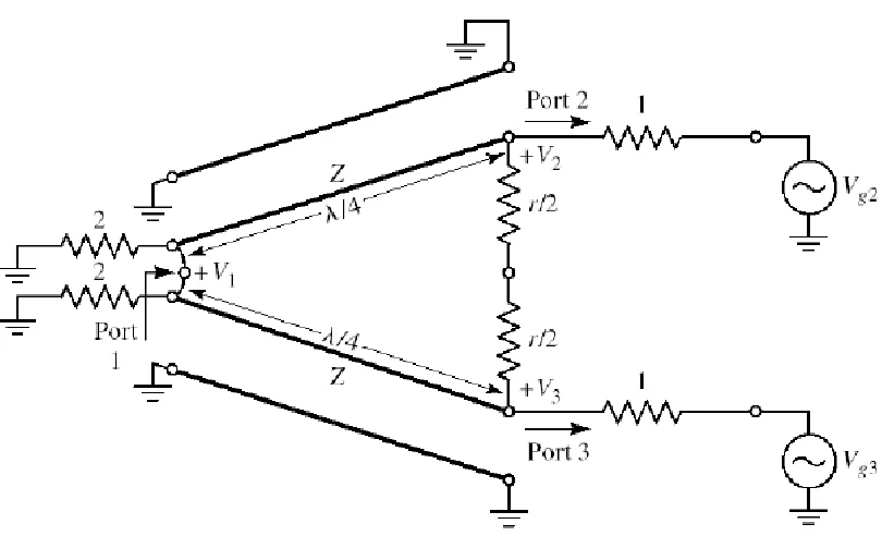
3.2.4 Wilkinson Power Divider
In 1960, Ernest Wilkinson proposed a Wilkinson power divider. This PD is capable of
Chapter 3 –Power Divider
54
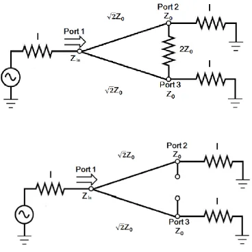
all the output ports are matched (Wilkinson, 1960). Figure 3.5 and Figure 3.6 shows the
microstrip and the equivalent transmission line circuit for the Wilkinson PD as taken from
(Pozar, 2011) where there is equal power division to the two output ports.
Figure 3.5 Equal-split Wilkinson power divider in microstrip form (Pozar, 2011)
Figure 3.6 Equivalent transmission line circuit (Pozar, 2011)
Wilkinson PD design is made up of microstrip or stripline transmission line that has been
55
his original proposal, each of