CIRCUITS
Thesis by
Jonathan Earl Green
In Partial Fulfillment of the Requirements for the
Degree of
Doctor of Philosophy
CALIFORNIA INSTITUTE OF TECHNOLOGY
Pasadena, California
2007
© 2007
Jonathan Earl Green
for Jennie
Acknowledgments
The first person I would like to thank is my advisor, Professor Jim Heath. I am grateful for
all of his support and guidance over the past four years, and more recently for his letters of
recommendation. I would also like to thank Jim for providing the resources that were
imperative for much of my research. It is no secret that Jim works tirelessly to secure
funding for our group, and only after writing this thesis can I begin to appreciate how
painful all that grant writing might have been.
The next person I would like to thank is my beautiful wife, Jennie, whom I met
during Caltech’s graduate student orientation week in September of 2002, and who has
been my closest friend ever since. I am grateful beyond words for her love, friendship,
support, and motivation. I can’t imagine going through graduate school (especially at
Caltech!) without her.
I would also like to thank my parents, Earl and Marianne Green, for their love,
support, and unwavering encouragement throughout the years. In addition, I am grateful for
the love and support of Jennie’s parents, Rudy and Sue Sanders.
I am grateful to all my colleagues and friends in the Heath group. In particular, I
would like to thank Jang Wook Choi, who was my partner on the memory project; Bonnie
Sheriff, whom I worked with on a number of projects, especially during my first year of
research; Ezekiel Johnston-Halperin, whom I worked with on just about every
nanowire-related project; Erica DeIonno, whom I worked with on the memory project; Rob
Beckman, whom I worked with on the demultiplexer project; and Yi Luo, who made
on nanofabrication. Also, I would like thank my office mates: John Nagarah, Habib
Ahmad, Ke Xu, Akram Boukai, and Yuri Bunimovich. Thanks to John for helping me get
the optical image of a molecular memory circuit decorated with white blood cells and to
Habib for the Photoshop work, and thanks to Akram, Yuri and Ke for their efforts on the
memory project. I would also like to thank Diane Robinson for her enduring assistance
with anything funding- or paperwork-related, not to mention and all the other little tasks
that made my life easier. Also, thanks to Kevin Kan for providing (literally) 24-hour
equipment assistance, even on weekends.
Thanks to my thesis committee: Prof. William Goddard, Prof. Mitchio Okumura,
and Prof. Nate Lewis, for their insights on my research.
Thanks to the J. Fraser Stoddart group, and in particular, to Hsian-Rong Tseng for
synthesizing the bistable [2]rotaxanes used in the molecular memory work.
Thanks to Bruce Brunschwig and the Caltech Molecular Materials Research Center
(MMRC) for assistance with XPS and MPMS measurements.
Thanks to Diane Buchness and Laura Howe (the former and present chemistry
graduate office representatives, respectively) for help with departmental paperwork,
especially during candidacy and graduation.
Thanks to Michelle Giron and Shelley Wong, whom I had the privilege of
mentoring as part of the Caltech SURF program.
Finally, I am grateful to all of my friends at Caltech, whom I found to be the
warmest and most intelligent group of people I have ever met. In particular, I would like
thank Eric Ostby and Jim Adleman, who have not only been great friends, but valuable
Abstract of the thesis
This thesis describes research towards the realization of large-scale, ultra-dense
nanowire-based circuits. The primary means for the construction of such circuits is the superlattice
nanowire pattern transfer (SNAP) technique. This technique was optimized for the
fabrication of large nanowire arrays containing over 1000 nanowires at narrow pitch and
aligned over millimeter length scales. Silicon nanowire arrays were fabricated with wire
widths down to ten nanometers, and with precisely-controlled electronic properties and
bulk-like resistivity values through the use of diffusion doping and the selection of
high-quality silicon-on-insulator substrates.
A binary tree demultiplexer circuit allows the unique addressing of N nanowires from within an ultra-dense array using of order 2×log2(N) control wires. An
implementation of this circuit was experimentally demonstrated to bridge from the
submicrometer dimensions of lithographic patterning to the nanometer-scale dimensions of
SNAP patterning. This circuit utilized field-effect gating by relatively large control wires to
address individual nanowires from within a 150-nanowire array patterned at a wire width
and pitch of 13 and 34 nanometers, respectively.
Silicon- and metal-nanowire arrays were integrated with [2]rotaxane molecular
materials for the fabrication of an ultra-dense, 160,000-bit crosspoint molecular electronic
memory circuit. This circuit is patterned at a record density of 1×1011 bits per square
centimeter (device-pitch of 33 nanometers), and contains bistable, electrochemically
individual crosspoint junctions. Defective junctions could be readily identified through
electronic testing and isolated through software coding. The working bits could then be
configured to form a functional memory circuit. The molecular-mechanical nature of the
switching mechanism was confirmed through volatility measurements.
An optimized two-step chlorination/methylation protocol was used to methyl
passivate thin (~20-nanometer) silicon(111)-on-insulator microelectronic device surfaces,
that were then demonstrated to be stable in air for arbitrarily long periods, and to resist
oxidation due to common microelectronic fabrication procedures and wet-chemical
treatments. Additionally, temperature-dependent mobility data showed that methylated
silicon-on-insulator surfaces can be prepared with bulk-like mobility characteristics
Table of contents
Acknowledgements ...iv
Abstract ...vi
Table of contents...viii
List of figures...xi
Chapter 1: Thesis overview...1
1.1 Nanotechnology and nanoelectronics ... 1
1.2 Organization of the thesis... 4
1.2.1 Fabrication of ultra-dense nanowire arrays ... 4
1.2.2 Demultiplexing ultra-dense nanowire arrays ... 6
1.2.3 Ultra-dense crossbar molecular electronic circuits ... 7
1.2.4 Covalent modification and electrical characterization of silicon (111)-on-insulator devices ... 8
1.3 References ... 9
Chapter 2: Fabrication of ultra-dense nanowire arrays...11
2.1 Introduction ... 11
2.2 The SNAP nanowire fabrication technique... 14
2.2.1 Introduction to SNAP... 14
2.2.2 Detailed description of SNAP nanowire fabrication... 16
2.2.3 Selective etching GaAs on AlGaAs... 20
2.2.4 Optimum platinum evaporation angle ... 24
2.2.5 Epoxy formulation ... 25
2.3 Achieving bulk-like conductivity of silicon nanowires ... 26
2.4 Silicon nanowire doping ... 32
2.5 Concluding remarks ... 39
Appendix 2.1: Experimentally determined doping data
for 25, 31 and 50 nm SOI... 42
Chapter 3: Demultiplexing ultra-dense nanowire arrays...45
3.1 Introduction ... 45
3.2 Demultiplexer architectures and alignment tolerance... 47
3.2.1 Alignment tolerance through architecture ... 51
3.2.2 Feature size tolerance through architecture... 52
3.3 FET-based demultiplexing of SNAP-fabricated NW arrays... 53
3.4 Demultiplexer patterning requirements ... 62
3.5 Demultiplexer fabrication ... 64
3.6 References ... 66
Chapter 4: Ultra-dense crossbar molecular memory circuits...68
4.1 Introduction ... 68
4.2 The [2]rotaxane switching cycle... 71
4.3 The crossbar architecture ... 75
4.4 [2]Rotaxane molecular electronic crossbar circuits ... 77
4.5 A 160,000 bit memory circuit patterned at 1×1011 bits/cm2... 80
4.6 Crossbar molecular memory circuit fabrication and testing ... 91
4.6.1 Fabrication and contact to bottom Si nanowire electrodes ... 92
4.6.2 Deposition of molecules and top electrode materials ... 99
4.6.3 Memory testing ... 106
4.7 Limitations of the SNAP process for crossbar circuits ... 111
4.8 Concluding remarks ... 113
4.9 References ... 114
Appendix 4.1: Details of lithographically-patterned structures ... 118
Appendix 4.2: Memory probe card specifications ... 122
Chapter 5: Covalent modification and electrical characterization
of silicon (111)-on-insulator devices...136
5.1 Introduction ... 136
5.1.1 Electrical properties of silicon surfaces... 136
5.1.2 Covalent modification of silicon (111) surfaces ... 142
5.1.3 Application to FET-based nanowire demultiplexers ... 143
5.2 Fabrication and methyl passivation of SOI devices ... 145
5.2.1 Silicon (111)-on-insulator wafer fabrication... 145
5.2.2 Hall bar fabrication... 147
5.2.3 Methyl passivation of SOI devices... 149
5.2.4 Making electrical contact to methyl-passivated devices... 151
5.3 Spectroscopic characterization of CH3-passivated SOI devices... 154
5.3.1 Measurement description... 154
5.3.2 Surface characterization data ... 155
5.4 Electrical characterization of CH3-passivated SOI devices ... 161
5.4.1 Introduction to low-field Hall measurements... 161
5.4.2 Measurement description... 164
5.4.3 Electrical characterization data... 169
5.5 Concluding remarks ... 173
List of Figures
Chapter 1
Figure 1-1 Schematic diagram of a crossbar architecture ... 3
Figure 1-2 False-colored SEM image of a molecular memory circuit ... 8
Chapter 2 Figure 2-1 Major steps in SNAP nanowire fabrication... 17
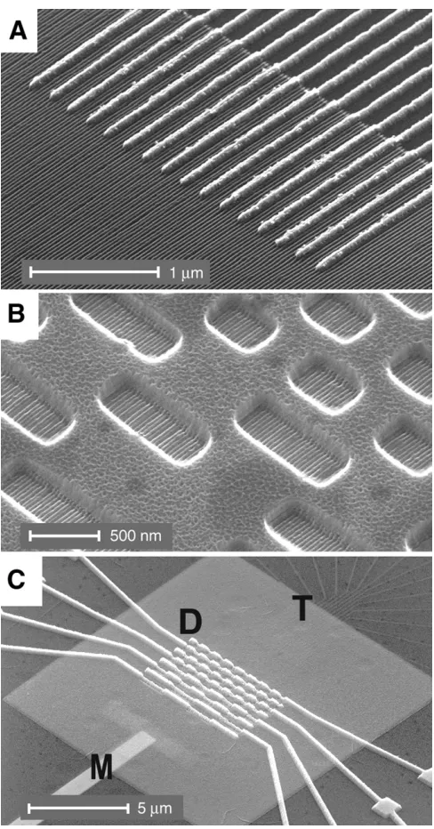
Figure 2-2 SEM images of SNAP nanowire fabrication... 18
Figure 2-3 Pt deposition onto an etched GaAs/AlGaAs template ... 21
Figure 2-4 SEM of a 400-nanowire GaAs/AlGaAs superlattice ... 23
Figure 2-5 Si nanowire electrical properties... 28
Figure 2-6 Electrical properties of Si(111) nanowires ... 30
Figure 2-7 P-type nanowire gating response ... 31
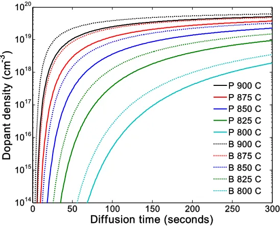
Figure 2-8 Calculated dopant concentrations vs. time and temp ... 35
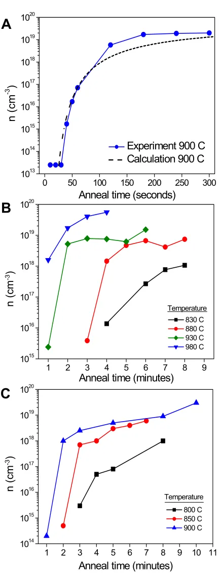
Figure 2-9 Time and temp. dependence of phosphorous doping in SOI ... 36
Figure 2-10 Dopant density vs. depth with and without dopant drive-in .. 37
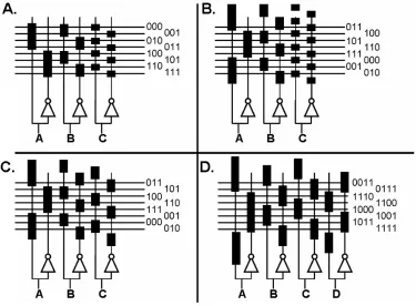
Chapter 3 Figure 3-1 Operation of a NOR logic binary tree demultiplexer... 50
Figure 3-2 Schematic nanowire demultiplexer for 32 Si nanowires... 54
Figure 3-3 Demultiplexer side-view and measured doping profile ... 56
Figure 3-4 Demultiplexer constructed on a test circuit ... 57
Figure 3-5 SEM of the nanowire demultiplexer assembly process ... 59
Figure 3-6 Operation of the demultiplexer for different input addresses .. 61
Figure 3-7 Illustration of the importance of alignment precision ... 63
Chapter 4 Figure 4-1 Schematic of a nanoelectronic crossbar circuit architecture .... 70
Figure 4-3 Bistable [2]rotaxane switching cycle... 73
Figure 4-4 False-colored image of memory circuit with blood cells... 81
Figure 4-5 SEM of the nanowire crossbar memory ... 84
Figure 4-6 Performance evaluation of a 128-ebit memory circuit... 86
Figure 4-7 Memory storage and retention characteristics... 90
Figure 4-8 Process flow for fabricating the 160,000 bit memory circuit... 93
Figure 4-9 SEMs illustrating the crossbar memory fabrication process.... 96
Figure 4-10 Conductance monitoring during Ti layer etching ... 101
Figure 4-11 Diagnostic Ti etching between EBL-defined microwires.... 103
Figure 4-12 SEM of a memory circuit before optimization... 105
Figure 4-13 Raw switching data ... 108
Figure 4-14 Data from a memory circuit with extensive shorting... 109
Figure 4-15 Next-generation memory circuits using SNAP... 112
Chapter 5 Figure 5-1 Surface states at a silicon interface ... 138
Figure 5-2 Schematic cross-section of a nanowire demultiplexer ... 143
Figure 5-3 Dopant density vs. depth for Si(111) epilayers ... 148
Figure 5-4 SOI chlorination/methylation reaction protocol... 150
Figure 5-5 AFM of a 40 nm Si(111) epilayer etched in NH4F ... 155
Figure 5-6 XP spectra of an H-terminated silicon epilayer... 156
Figure 5-7 XP spectra of a methyl-terminated SOI surface in air... 157
Figure 5-8 CH3-SOI surfaces after various chemical treatments... 160
Figure 5-9 Hall measurement circuit ... 166
Figure 5-10 Hall and longitudinal voltages vs. magnetic field ... 168
Figure 5-11 Resistivity and Hall mobility of highly-doped devices... 170
Figure 5-12 Mobility as a function of PCl5 chlorination time ... 171
Figure 5-13 A CH3-SOI device chlorinated by 10 minutes in PCl5... 171
Chapter 1
Thesis overview
1.1 Nanotechnology and nanoelectronics
The rapidly expanding fields of nanoscience and nanotechnology are within the midst of
an extraordinary period of scientific and technological productivity, due in no small part
to the unprecedented collaboration of researchers from across the physical, chemical,
biological, and life sciences. The promise of functional systems at the nanometer (nm)
length scale (1–100 nm) has spurred researchers in diverse disciplines to engage in
fruitful collaborations across traditional academic boundaries and between academia,
industry, and government1. The result has been a modern-day scientific renaissance as the
talents of chemists, physicists, biologists and engineers are simultaneously leveraged to
understand and exploit novel phenomena and functionality particular to the nanometer
size regime. Emerging applications of nanotechnology range from ultra-dense
information storage2 to sustainable water purification3, to in-vivo biological sensorsand intelligent drug delivery systems4, to ‘smart materials’ capable of sensing changes to their
external environment and responding accordingly5.
An exciting sub-field of nanotechnology is nanoelectronics and, in particular,
technologies and materials systems currently in use by the semiconductor
microelectronics industry cannot sustain the forty-year-old trend of device
miniaturization into the coming decades. Indeed, the microelectronics industry had to
overcome significant technical barriers to achieve the sub-100-nanometer dimensions of
today’s transistors, and such barriers are becoming increasingly numerous and more
difficult to overcome as device dimensions continue to shrink. This is highlighted by a
recent assessment7 of the technology requirements for future generations of integrated
circuits, which forewarns the emergence of insurmountable technical barriers (either
physical or economical) by as early as the year 2010.
This has led to a growing consensus that continued improvements in
computational technology will likely occur through the development of alternative
materials, patterning methods, and architectures7, 8. To that end, the Heath group began a
research program with the intent to develop the required materials, methods, and circuit
architecture to construct an ultra-dense molecular electronic computer. The Heath group
‘vision’ for such an integrated circuit is shown in Figure 1-1. The dominant theme of this
circuit is the crossbar architecture6, which consists of two perpendicularly overlaid arrays
of high-density nanowires. These nanowires tile together the various computational
elements of the circuit (logic, memory, etc.), which are themselves derived from unique
electrically active thin-film materials sandwiched between the nanowires at the locations
shown in the figure.
My research has focused on a number of the components shown in Figure 1-1 for
realizing this multifunctional computational architecture. These have included the
Figure 1-1. Schematic diagram of a nanoelectronic crossbar architecture. The various computational elements such as memory, logic, and routing are shown tiled together through nanowire arrays. Multiplexers (Mux) and/or demultiplexers (Demux) control signals within the circuit and to outside electronics (power I/O).
Logic
Logic Routing &
Amplification Routing & Amplification Memory Memory Mux/Demux Mux/Demux Mu x/ D emu x Mu x/ D emu x
Control I/O
Pow er I/ O Pow er I/ O Power I/OPower I/O Power I/OPower I/O
Mu x/ D em ux Mu x/ D em ux Mu x/ D em ux Mu x/ D em ux Routing & Amplification Routing & Amplification Mux/Demux Mux/Demux Mux/Demux Mux/Demux Mux/Demux Mux/Demux Mu x/ D em ux Mu x/ D em ux Po w er I /O Po w er I /O
with precisely controlled electronic properties (Chapter 2), the demonstration of a
field-effect transistor (FET)-based demultiplexer capable of bridging from the sub-micrometer
length scales of conventional silicon microelectronic technology to the nanometer length
scales of molecular electronics (Chapter 3), the integration of sub-lithographic patterning
techniques and molecular materials for the fabrication of ultra-dense molecular electronic
memory circuits (Chapter 4), and molecular-level control over nanoelectronic device
1.2
Organization of the thesis
To accommodate the largely independent, but closely related, projects which have
comprised my graduate research in the Heath group at Caltech, I have chosen to organize
this thesis into chapters—with each chapter completely self-contained and with its own
background and references. The following sections will provide a brief overview the
chapters in this thesis, summarizing the main results of the research described in each
chapter and (hopefully) providing some overall unity to the topics discussed individually
in the chapters.
1.2.1
Fabrication of ultra-dense nanowire arrays
In Chapter 2, I describe research directed towards the development of high-quality arrays
of silicon and metallic nanowires. One-dimensional nanostructures such as nanowires are
useful in a wide variety of applications in nanotechnology9, and have emerged as the
fundamental building blocks of novel nanoelectronic circuits. Such structures can be
fabricated using highly parallel techniques and assembled into ultra-dense
crossed-nanowire (crossbar) circuits such as shown in Figure 1-1. Nanowires not only propagate
electrical signals throughout the circuit, but can also serve as the active components
within the circuit. This dual functionality results in significant savings in wiring overhead,
and enables crossed-nanowire circuits to be fabricated at the incredible densities I
There are a number of methods for the fabrication of silicon nanowires, with most
based on the catalytic growth of nanowires from molecular precursors9. However, this
technique has a number of significant drawbacks for application to large-scale
nanoelectronic circuitry. For one, crossbar circuits fabricated from catalytically-grown
nanowires are usually limited in size to around 10 micrometers, and to date have
contained at most 100 junctions10. Additionally, the techniques required to align
catalytically-grown nanowires are rather complicated and generally imperfect. This
makes their integration with lithographically-defined structures such as binary tree
decoder circuits (discussed in Chapter 3) awkward and difficult. Dr. Nick Melosh, a
former post-doc in the Heath group, developed a method in which high-density arrays of
silicon or metal nanowires could be patterned without such a limitation. This method is
called the superlattice nanowire pattern transfer, or SNAP, technique and allows the
fabrication of dense arrays of nanowires aligned over millimeter length scales.
Chapter 2 describes my efforts to systematically remove much of the
phenomenology that had previously plagued the SNAP technique and the extension of
SNAP to higher-density and larger-element arrays of nanowires. In addition, Chapter 2
will describe my efforts in developing reliable doping protocols and eliminating
fabrication-induced nanowire defects to achieve bulk-like conductivity characteristics
1.2.2
Demultiplexing ultra-dense nanowire arrays
The SNAP technique is capable of producing arrays of metal and silicon nanowires with
dimensions (width and pitch) beyond the capabilities of conventional lithographic
techniques. However, such dense circuitry provides a new challenge for the field of
nanoelectronics, namely, how to electrically address circuits that have characteristic wire
dimensions and pitches that are smaller than the resolution achievable through
lithographic patterning. The selective addressing of, and interaction with, individual
nanostructures at high densities is one of the central challenges of both nanoscience and
nanotechnology—in the absence of a resolution to this problem, many of the potential
benefits of these emerging fields will remain unrealized. For instance, the
nanowire-based molecular electronic memory circuit described Chapter 4 is nearly two orders of
magnitude denser than conventional circuitry. However, the lack of a robust technology
to selectively address individual nanowires from within an ultra-dense array reduces the
effective density of such a circuit to that of conventional (lithographically-defined)
circuitry.
Chapter 3 describes research by my co-workers (Dr. Robert Beckman, Dr. Ezekiel
Johnston-Halperin and Dr. Yi Luo) and me to demonstrate a FET-based nanowire
demultiplexing architecture that can be patterned with significantly larger dimensions
than the nanowires it addresses, and with wide alignment tolerances. Its shown that this
architecture successfully interfaces with high-density SNAP-fabricated nanowires to
bridge the dimensional gap between nanometer-scale circuitry and conventional
1.2.3
Ultra-dense crossbar molecular electronic circuits
In 2002, the Heath group reported on the use of bistable [2]rotaxane molecules as the
active elements within a 64-bit molecular electronic random access memory (RAM)
circuit that utilized micrometer-scale wiring12. Although this work successfully
demonstrated that molecules could be used store information within a solid-state crossbar
circuit, it did not take advantage of the unique scalability offered by molecular
components.
Chapter 4 is devoted to what has comprised the majority of my research efforts in
the Heath group, namely, the integration of SNAP-fabricated arrays of silicon and metal
nanowires with molecular materials for the fabrication of an ultra-dense, 160,000-bit
molecular electronic crossbar memory circuit patterned at a record density of 100 gigabits
per square centimeter (1×1011 bits cm–2)13. The construction of this memory circuit was a
true tour de force in nanofabrication that would not have been possible without the efforts my colleague, Jang Wook Choi. In addition, numerous other members of the Heath and
Stoddard group (at UCLA) made important contributions to this effort13.
Beginning with a description of the rich science underlying the switching
mechanism of bistable [2]rotaxane molecules and their integration into high-density
crossbar architectures, Chapter 4 covers, in depth, the fabrication and operation of the
memory circuit. The work described in this chapter shows that molecules can be used as scale-invariant components in solid state circuitry and, moreover, that functional circuitry
Figure 1-2. A false-colored scanning electron micrograph of a molecular electronic memory circuit fabricated from [2]rotaxane molecular materials and SNAP-fabricated silicon and titanium nanowires. The memory region is defined by the intersection of 400 silicon nanowires (light blue) and 400 titanium nanowires (light yellow), and contains 160,000 bits in an area of 13×13 square micrometers (or 1×1011 bits per square centimeter).
1.2.4
Covalent modification and electrical characterization of
silicon-on-insulator devices
As the feature sizes of silicon devices continue to be scaled towards nanometer
dimensions, the physical and chemical properties of the surface play an increasingly
prominent role in determining the overall device behavior. This has presented significant
challenges, and opportunities, to the nanotechnology community, where surface effects
manifest over a range of applications from nanoelectromechanical systems (NEMs)14 to
Covalent alkyl passivation of silicon surfaces is attractive for a variety of
nanoelectronic applications, such as FET-based demultiplexing and molecular electronics.
However, the majority of work with alkyl-passivated, (111)-oriented silicon surfaces has
utilized bulk wafers. While such wafers are convenient for surface characterization
studies, they are less useful for the nanoelectronic applications of interest to us, where
SOI structures are generally required. This last chapter of my thesis describes ongoing
work to obtain high-quality methyl passivation of ultra-thin (111)-oriented SOI devices
and their subsequent electrical characterization using variable-temperature conductivity
and mobility measurements. Using an optimized (for SOI devices) version of the surface
methylation protocols developed by the Lewis group at Caltech16, robust methyl
passivation of silicon surfaces was achieved with devices as thin as 20 nanometers thick.
Chapter 5 presents data showing that this passivation is resistant to oxidation for
extended periods of time in ambient air, and after exposure to an assortment of common
nanofabrication procedures and chemical treatments. Additionally,
temperature-dependent mobility data shows that methylated ultra-thin surfaces can be prepared with
bulk-like mobility characteristics.
1.3 References
1. Hassan, M. H. A. Nanotechnology: Small Things and Big Changes in the Developing World. Science 309, 65–66 (2005).
2. Galatsis, K. et al. Emerging memory devices — Nontraditional possibilities based on nanomaterials and nanostructures. Ieee Circuits & Devices 22, 12–21 (2006). 3. Savage, N. & Diallo, M. S. Nanomaterials and Water Purification: Opportunities
4. Ferrari, M. Cancer Nanotechnology: Opportunities and Challenges. Nature Reviews Cancer 5, 161–171 (2005).
5. Altmann, J. & Gubrud, M. Anticipating military nanotechnology. Technology and Society Magazine, IEEE 23, 33–40 (2004).
6. Heath, J. R. & Ratner, M. A. Molecular electronics. Physics Today 56, 43–49 (2003).
7. The International Technology Roadmap for Semiconductors (ITRS), 2005 Edn. San Jose, CA, Semiconductor Industry Association.
8. Cavin, R. K. et al. A long-term view of research targets in nanoelectronics. Journal of Nanoparticle Research 7, 573–586 (2005).
9. Lu, W. & Lieber, C. M. Semiconductor nanowires. Journal of Physics D–Applied Physics 39, R387–R406 (2006).
10. Whang, D., Jin, S., Wu, Y. & Lieber, C. M. Large-scale hierarchical organization of nanowire arrays for integrated nanosystems. Nano Letters 3, 1255–1259 (2003). 11. Beckman, R., Johnston-Halperin, E., Luo, Y., Green, J. E. & Heath, J. R. Bridging
dimensions: Demultiplexing ultrahigh-density nanowire circuits. Science 310, 465–468 (2005).
12. Luo, Y. et al. Two-dimensional molecular electronics circuits. ChemPhysChem 3, 519–525 (2002).
13. Green, J. E. et al. A 160-kilobit molecular electronic memory patterned at 1011 bits per square centimetre. Nature 445, 414–417 (2007).
14. Wang, Y., Henry, J. A., Sengupta, D. & Hines, M. A. Methyl monolayers suppress mechanical energy dissipation in micromechanical silicon resonators. Applied Physics Letters 85, 5736–5738 (2004).
15. Zhang, P. et al. Electronic transport in nanometre-scale silicon-on-insulator membranes. Nature 439, 703–706 (2006).
Chapter 2
Fabrication of ultra-dense nanowire
arrays
2.1 Introduction
The development of arrays of semiconducting and metallic nanowires (NWs) will
undoubtedly be important for the realization of any future nanoelectronic circuit
architecture. NWs serve to not only propagate electrical signals into and out of a circuit,
but can also function as the active components within the circuit. For example, NWs have
been used to fabricate nanoscale field-effect transistors (FETs)1-6, p-n diodes7, 8, bipolar
junction transistors7, nanoscale electro-mechanical oscillators9, 10, lasers11, LEDs12,
complex logic gates13, and complementary inverters with signal gain14. This economy of
functionality makes NWs an ideal building block for assembling larger and
more-complicated nanoelectronic circuits since the fabrication of such circuits can be
accomplished with little additional complexity15. For instance, aligned arrays of NWs can
be used to fabricate a crossbar structure (an expanded ticktacktoe board) by repeating the
NW fabrication procedure twice with the second set of NWs fabricated on top of, and
perpendicular to, the underlying first set of NWs. By implementing a computational
circuit containing N × M electronic devices can be fabricated from two constituent N- and
M-nanowire arrays. The device-to-device pitch is limited by the pitch of the NWs, so the ultimate density of a NW crossbar circuit is limited by the dimension and pitch of the
technique used to form the NW arrays. This has driven researchers in the field to develop
methods for assembling NW arrays at very narrow pitch. The scalability and
manufacturability of crossbar circuits has lead to an emerging consensus that future
nanoelectronic applications (not necessarily limited to conventional computational
functions, such as memory and logic) will most likely be based on the crossbar
architecture16-19.
In addition to NWs, single-walled carbon nanotubes (SWNTs) have gained
considerable attention from the nanotechnology community. Carbon nanotubes are
cylindrical, rolled-up sheets of graphene that are about a nanometer in diameter and
possess remarkable electronic, thermal, and mechanical properties (excellent reviews are
available from Hongjie Dai20 and Paul McEuen21). Current synthesis techniques produce
a mix of semiconducting and metallic nanotubes (with about two-thirds being
semiconducting), and while great progress has been made to separate the two22, nanotube
electronics continues to be hindered in the absence of a high-throughput separation
technique. This is in contrast to semiconductor NWs, where the electrical properties can
be precisely controlled through doping. In addition, NW length, width, and morphology
can be tailored during fabrication. Considerations such as these have made
semiconducting NWs the dominant structure for building nanoelectronic circuits
For electronics applications, the semiconducting material of choice is silicon. The
physical and mechanical properties of silicon have been well characterized and there are
highly developed protocols for patterning and electrically contacting silicon devices. An
additional benefit is the possibility of integration onto a conventional CMOS technology
platform, thus opening the door for relatively near-term commercial applications.
The versatility of Si NW-based electronics has fueled intense research and
development of semiconductor NW fabrication protocols to enable the parallel
fabrication of large numbers of NWs of specific geometry and with precisely controlled
electrical properties.
The most widely used Si NW fabrication technique is the vapor-liquid-solid
(VLS) growth mechanism23, 24. A typical procedure is to heat a gold nanocluster in the
presence of vapor-phase silicon (usually SiH4 in an H2 carrier gas) to the Au-Si eutectic
temperature (363° C), resulting in the formation of a liquid droplet of Au-Si alloy. As
vapor-phase silicon is continuously fed into the reaction chamber, the droplet becomes
supersaturated and solid silicon precipitates out of the melt. As long as there is silicon
precursor in the reaction vessel to keep the droplet supersaturated, a Si NW grows from
the solid-liquid interface with the supersaturated droplet riding on top. This process can
be fine tuned to produce Si NWs with reasonably well controlled lengths and diameters25
(which is primarily determined by the diameter of the Au catalyst). However, the VLS
NW fabrication technique faces some significant challenges. VLS-grown NWs tend to be
limited in length to around 10 micrometers (μm)26, which in turn limits their practical
applicability to anything other than small-scale nanoelectronic circuits. The precise
since the NWs are doped in-situ by adding dopant precursor to the reaction vessel. Additionally, while the VLS technique can be used fabricate large numbers of NWs in
parallel, subsequent procedures are required to align the NWs into arrays and crossbar
circuits24. The most successful procedure to date employs a Langmuir-Blodgett (LB)
trough27 to align the NWs parallel to one another. However, this technique suffers from
fluctuations in the average alignment direction and poor end-to-end registry of individual
NWs. This makes interconnecting and integrating such arrays into larger (especially
CMOS-compatible) circuitry difficult. In addition, the LB technique would be difficult to
scale-up for the commercial manufacture of NW circuits.
2.2 The SNAP nanowire fabrication technique
2.2.1 Introduction to SNAP
The ability to assemble nanoscale building blocks such as Si NWs into integrated
nanoelectronic structures at narrow pitch (and therefore high density) is a general
challenge in nanotechnology. The majority of work in the field has focused on
few-device demonstrations of scaling feature size, and has largely neglected such
considerations as feature pitch, device-to-device reproducibility, and manufacturability—
all of which are required for any robust application. The superlattice nanowire pattern
transfer (SNAP) technique was developed within the Heath group10 to simultaneously
address these issues. The SNAP technique is a ‘top-down,’ non-photolithographic
(length-to-width ratio routinely > 106) Si and/or metal NWs that are aligned over millimeter length
scales, and without the need for a secondary alignment step after NW fabrication. NW
width and wire-to-wire pitch are highly reproducible and the technique is compatible with
conventional CMOS technology and adaptable for large-scale manufacturability.
Furthermore, the SNAP technique permits precise control of the electrical characteristics
of Si NWs through quantitative doping control. These traits make the SNAP technique
ideally suited for realizing large-scale NW circuits.
My initial research efforts in the Heath group were devoted to optimizing the
SNAP procedure so that fabrication of Si NW arrays with precisely controlled electrical
properties would be routine and reproducible. Previous efforts were successful in using
SNAP to generate arrays of 128 Si NWs of widths down to 20 nm, but only a fraction of
those NWs conducted, and none exhibited bulk-like conductivity characteristics10. We
found that Si NWs of widths of less than 30 nm are critically sensitive to the defects
introduced by standard processing methods such as ion-implantation doping. Nanowires
significantly smaller than 50 nm in width (~25-nm thick) and longer than 10 μm will
often contain at least one such defect, and the result is a poorly conducting wire.
However, by moving to diffusion doping we were able to improve the conductivity of our
Si NWs by a factor of 103, and to demonstrate that Si NWs with diameters of 10 nm and
lengths in excess of 1 mm can be fabricated with controllable, bulk-like conductivity
characteristics and useful field-effect transistor properties28. In what follows I will
describe the efforts of my coworkers and I to optimize SNAP NW fabrication procedures
memory circuits, in addition to achieving bulk-like conductivity from SNAP-fabricated
Si NWs. I will begin with a general description of the SNAP NW fabrication protocol.
2.2.2
Detailed description of SNAP nanowire fabrication
SNAP uses molecular-beam epitaxy (MBE) to create a physical template for NW
patterning. This template is a custom-grown gallium arsenide/aluminum gallium arsenide
(GaAs/AlxGa(1-x)As) superlattice structure consisting of alternating layers of GaAs and
AlxGa(1-x)As grown on top of a (100) GaAs substrate. The mole fraction x ranges from 0.5
to 0.8; for clarity, the subscripts will be omitted in what follows. For typical applications,
the AlGaAs layer thickness determines the NW width and the GaAs layer thickness
determines the separation between NWs. Because MBE is capable of growing layers with
atomic resolution, the NW width and separation can in principle be reduced to just a
couple of atomic layers. In practice, however, NWs have been limited to about 7–8 nm in
width and 15 nm in pitch29, although, as of this writing, we haven't pushed very hard on
this limit.
The number of alternating layers of GaAs and AlGaAs determines the number of
NWs in the array. To date, we have successfully used the SNAP technique to fabricate
arrays containing up to 1400 NWs29; however, there is no reason (in principle) why we
couldn’t increase this number considerably.
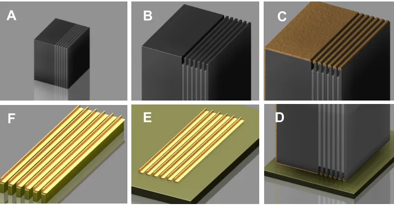
The SNAP fabrication protocol begins by carefully dicing a portion of the
superlattice wafer into small rectangular pieces approximately 2 mm wide and 5 mm long
(Figure 2-1.A). These pieces will henceforth be referred to as masters for reasons that
A
B
C
D
E
[image:29.612.125.524.81.290.2]F
Figure 2-1. The major steps in SNAP nanowire fabrication (clockwise direction) A. A small piece of the GaAs/AlGaAs superlattice is selectively etched, B, forming a comb-like structure. C. Pt is then deposited along the ridges of the comb. D. The superlattice template is adhered to an epoxy-coated thin-film substrate. E. The superlattice is released from the Pt nanowires and, F, the Pt nanowire pattern is transferred into the underlying thin film.
such that one of the 2-mm-wide edges of the master is precisely along a lattice direction.
This leaves an atomically flat {110} or {001} plane exposed on that edge (depending on
the direction of cleave). The masters are then loaded into a custom-made Teflon holder
with the atomically flat edge facing up. They are sonicated in methanol (~10 seconds at a
time) and the atomically flat edge is gently swabbed until all particulates visible under a
160× magnification optical microscope are removed. The superlattice region of the
master is scrupulously cleaned before proceeding since a single micrometer-sized piece
of debris can (and frequently does) result in unsuccessful NW fabrication. I have found
that small particulates relatively far away from the superlattice region are not usually a
problem and can be ignored. Also, particulates that cannot be removed from sonication
The GaAs (or AlGaAs) layers
are selectively etched in an NH4
OH-H2O2 etch solution to form a
comb-like structure (Figures 1.B and
2-2.A) and 10 nm of Pt is then
deposited with the superlattice
surface oriented at 45° with respect
to the evaporative flux of an
electron-beam-evaporated Pt source
(Figure 2-1.C). The orientation of the
superlattice determines how much
metal is deposited along the ridges of
the AlGaAs (or GaAs) comb, which
defines the Pt NW template. The
metal-coated superlattice is then
applied to a thin (~10 nm) layer of
heat-curable epoxy spun onto a
substrate with a thin-film epilayer (Figure 2-1.D). To ensure that the epoxy spins down
uniformly, the surface is rigorously cleaned beforehand. The epoxy is then baked in two
steps for 10 minutes and 30 minutes at approximately 100° C and 135° C, respectively.
After curing, excess epoxy is removed by a high-power, 100-Watt (W) oxygen
reactive-ion etch (RIE) at 5 milliTorr (mTorr). The superlattice template is released from the Pt
NWs by etching the GaAs/AlGaAs superlattice in either commercially available
gold-A
400 nm
B
[image:30.612.111.337.94.379.2]1 μm
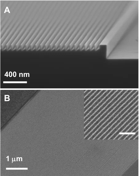
Figure 2-2. Scanning electron microscope (SEM) images of SNAP nanowire fabrication. A. Partially etched GaAs/Al0.5Ga0.5As superlattice
showing the Al0.5Ga0.5As ridges forming the Pt
etch solution (4 g KI + 1 g I2 into 100 ml H2O) or 1:5:50 solution of 30% H2O2 to conc.
H3PO4 to H2O; both for 3–5 hours*. The epoxy between the Pt wires is subsequently
removed in another oxygen RIE step (40W, 5 mTorr).
At this stage the SNAP procedure has produced an array of Pt NWs adhered to a
thin-film substrate (Figure 2-1.E). The Pt NWs can then be used as an etch mask in an
anisotropic RIE to transfer the NW pattern into the thin-film substrate (Fig 2-1F). The
highly versatile SNAP technique can be used to fabricate NWs out of any thin-film
material that can be anisotropically dry-etched. To fabricate Si NWs, the Pt NW pattern is
adhered to a doped silicon-on-insulator substrate. High-fidelity pattern transfer with
vertical side walls is accomplished using a high-frequency RIE tool (40 MHz Unaxis
SLR parallel-plate RIE) and fluorine-based reactive-ion etching at low substrate bias (10–
20 volts DC). An etch recipe of CF4, He, and H2 (20:30:2.5) at 40 W and 5 mTorr was
found to give vertical Si sidewalls with no observable undercut. (The added hydrogen
promotes the deposition of a fluoropolymer on the Si NW sidewalls to prevent
undercutting.) However, I found that this etch would occasionally reduce the conductivity
of boron-doped NWs. One possible explanation is that hydrogen in the etch was diffusing
into the NWs and forming a boron-hydrogen complex30. This complex results in
passivation of the dopant so it can no longer produce free charge carriers. For thin Si
epilayers, I have found this problem can be avoided without altering the etch fidelity by
simply removing H2 from the recipe. The Si etch end-point is determined by
interferometry, although the etch efficiency may be lower between the narrow-pitched Pt
NWs than where the actual laser spot is positioned (due to residual epoxy and Pt NW
* A lower bound for the etch time is given by (thickness of superlattice region)/etch rate. The phosphoric
charging effects). To ensure complete transfer of the Pt NW pattern into the underlying Si
film, the etch time is usually extended by 25–50 percent. Over-etching is not a problem
for most applications since this only results in transferring the NW pattern into the
underlying oxide by a small fraction (CF4 etches Si and SiO2 equally31 in pure CF4). After
transferring the Pt NW pattern to the underlying Si epilayer, the final step is to remove
the Pt NWs in hot aqua regia (1:4 conc. HCl to conc. HNO3 at 120° C, ~10 min). The
result is an array of Si NWs on an insulating oxide that are aligned and continuous over
hundreds of microns (Figure 2-1.E & Figure 2-2.B).
The selective GaAs etch, Pt evaporation angle, and epoxy formulation are all key
for obtaining high-quality NW arrays. Accordingly, I will discuss each in more detail
below.
2.2.3
Selective etching of GaAs on AlGaAs
The SNAP technique relies on a physical template for NW fabrication. The construction
of this template requires not only the fidelity of MBE to define alternating layers of GaAs
and AlGaAs, but the ability to etch GaAs with high selectivity. One of my goals was to
optimize this etch for various GaAs/AlGaAs superlattice structures. Although I will only
consider the selective etching of GaAs over AlGaAs, as an alternative AlGaAs can be
selectively etched over GaAs10 using a buffered-oxide etch solution (BOE) (6:1 NH4F to
HF). Selective etching of AlGaAs is generally avoided because BOE is hazardous to
work with. However, the ability to alternatively etch AlGaAs instead of GaAs can be
A
[image:33.612.115.340.150.465.2]B
Figure 2-3. Pt deposition onto an etched GaAs/AlGaAs template. A. Cross-sectional diagram of a portion of the etched GaAs/AlGaAs template. Pt is evaporated onto the AlGaAs ridges at an angle θ forming an upside-down ‘L’ structure (right-side up after depositing the Pt NW array) with base and edge thicknesses b and e, respectively. Pt coats one side of each AlGaAs sidewall to a depth, h, that depends on θ and the AlGaAs spacing, s. B. Calculated dimensions of the Pt ‘L’ as a function of θ for a superlattice with AlGaAs spacing s = 17 nm and evaporated Pt thickness t = 10 nm. The evaporation angle is chosen to give the best Pt nanowire morphology within the constraint that h is less than the GaAs etch depth, d. For the superlattice considered here, this is 45° (see text).
0 15 30 45 60
0 10 20 30
Evaporation angle θ
Na n o m et er s
Pt depth into GaAs recess (h)
base of 'L' thickness (b)
edge of 'L' thickness (e)
Pt
GaAs
AlGaAs
s
t
h
d
e
b
θ
Pt flux Pt ‘L’
The GaAs etch must be highly selective to GaAs over AlGaAs so that the AlGaAs
ridges of the comb are not rounded. It also needs to be controllable so that the etch
parameters can be calibrated to
produce a consistent etch depth.
The optimal etch depth is
dependent on the GaAs layer
thickness and the Pt
evaporation angle. This can be
seen from the cross-sectional
schematic of a GaAs/AlGaAs
comb shown in Figure 2-3.A.
Each AlGaAs ridge acts as a
self-aligned shadow mask for
the ridge behind it. Since the
evaporation angle must always
be less than 90° to avoid
depositing metal into the GaAs
recess, the Pt lines actually
have an ‘L’ structure, where the
dimensions of the ‘L’ depend
on the angle of evaporation
(Figure 2-3.B). The metal
AlGaAs ridge into the GaAs recess (h in Figure 2-3.A) for all relevant evaporation angles (i.e., 0° < θ < 90°) and increases with both the evaporation angle (Figure 2-3.B, black line) and the spacing of the AlGaAs layers. For maximum applicability to different
superlattices and varying evaporation angles, it is desirable for the GaAs etch to produce
a GaAs recess as deep as possible.
I explored two etch chemistries* and a range of etch concentrations on
superlattices containing 128, 150, and 400 alternating layers of GaAs/AlGaAs with layer
thicknesses of 10 nm/20 nm, 10 nm/25 nm, and 15 nm/20 nm, respectively. The 128- and
150-wire superlattices were grown by University of California Santa Barbara with mole
fraction of Al x = 0.5. The 400-wire superlattices were grown from either University of California Santa Barbara or IQE Inc. (Bethlehem PA) with mole fraction of Al x = 0.8. The two etch solutions were 1:20 conc. NH4OH to 30% H2O2[32] and 5:1 50% aqueous
citric acid (C6H8O7) to 30% H2O2[33, 34]. Aqueous citric acid was prepared by dissolving 1
gram of anhydrous C6H8O7 per milliliter of H2O. These stock solutions were diluted by
varying margins in H2O before use. Extra wide masters (about 4–5 mm) were cleaved
from a given superlattice along a lattice direction and subsequently etched for times
ranging from 5 seconds to 20 seconds, then rinsed with de-ionized (DI) (18 MΩ) water,
and dried under N2. After etching, each master was cleaved lengthwise into halves and
loaded onto a scanning electron microscope (SEM) puck with one piece laid on its side
with the fresh cleave facing up. This way a top-down view showing the registry of the
AlGaAs ridges as well as a cross-sectional view to measure the etch depth could be
obtained from the same master. Figure 2-2.A was generated in this fashion.
* An acetic acid-based etch was also tried but was found to be inferior to the NH
Both of the etch solutions were found to have excellent selectivity for GaAs over
AlGaAs. While the citric-acid etch in dilutions ranging from undiluted to 1:5 (stock
solution to H2O) and etch times from 6 to 30 seconds, respectively, produced good results
for the 128-wire superlattice, we found the NH4OH-H2O2 etch solution diluted by a factor
of 15 in H2O to be easier to prepare and more consistent from one run to another and for
different superlattices. Using this etch solution, the maximum (reliable) GaAs etch depth
was found to be 30–40 nm, corresponding to 10–12 seconds of etch time. Longer etch
times occasionally resulted in collapsed or broken-off AlGaAs ridges.
After etching the IQE-grown 400-wire superlattice in NH4OH-H2O2 solution, I
frequently observed small aggregates (< 50 nm) of what appeared to be solid Ga on the
superlattice surface (Figure 2-4). This excess Ga may originate from a Ga-rich
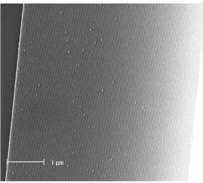
[image:35.612.176.469.409.673.2]reconstruction35 of the exposed {001} crystal plane after cleaving along the 〈110〉
Figure 2-4. Scanning electron micrograph (SEM) of a freshly-etched 400-nanowire GaAs/AlGaAs superlattice. This master was not treated with an additional H2O2 dip, and
direction (the direction along the IQE wafer flat). I found these aggregates could be
oxidized and removed from the superlattice surface by a 5-second dip in undiluted 30%
H2O2 immediately following the NH4OH-H2O2 etch. Although Ga aggregates on the
superlattice surface were found to be present only after cleaving along the 〈110〉 or 〈010〉
directions, the extra H2O2 treatment was adopted as a standard step in the NH4OH-H2O2
etch procedure. (In the very least, this step helped to remove particulates from the
superlattice surface.)
2.2.4
Optimum platinum evaporation angle
In addition to the GaAs etch, I systematically investigated how different Pt evaporation
This roughness is likely due to the accumulation of Pt
lt of the small evaporation angle (Figure
2-3.B, red line). Larger evaporation angles gave smoother Pt NWs, but to also increased the
depth of evaporated Pt along AlGaAs ridges (Figure 2-3.B, black line). After some trial and error, I found that a 45° evaporation angle worked the best. A 45° angle consistently angles affected the Pt NW morphology. Smooth Pt NWs are important because they must
serve as a high-fidelity stencil to define arrays of Si or other thin-film material NWs.
Ideally, Pt should only deposit along the AlGaAs ridges so that the transferred Pt NWs
are as symmetrical as possible. This requires a small evaporation angle to reduce the
depth of evaporated Pt along the side of individual AlGaAs ridges (Figure 2-3.B, black
line). However, this was found to also increase the roughness of transferred Pt NWs
along their corresponding side.
produces smooth Pt NWs while being shallow enough that evaporated Pt does not reach
the bottom of the GaAs recess (Figure 2-3.B).
2.2.5
Epoxy formulation
Optimizing the epoxy formulation for high-yield SNAP-NW fabrication has proven to be
quite difficult, and numerous members of the Heath group have worked to establish a
reliable formulation. In fact, one of my initial efforts in the Heath group was to
investigate the use of amine-terminated self-assembled monolayers (SAMs) on silicon to
replace the epoxy altogether as a Pt NW adhesive. We found that SAMs could produce
small arrays of aligned Pt NWs over distances of up to 50 μm, but reliable alignment over
longer distances and larger NW arrays was very difficult. To date, two epoxy
rmulations are used in the Heath group; both are modifications of Epoxy Bond 110
Dominguez California). Both formulations include a
olymeric additive that functions as a plasticizer to make the epoxy easier to etch in the fo
(Allied High Tech, Rancho
p
oxygen plasma steps described above. The first version uses a PMMA additive (0.37 g of
6 % PMMA, 20 drops of Epoxy Bond part A, 2 drops of Epoxy Bond part B, 15 ml of
chlorobenzene). This epoxy recipe etches easily in O2 but does not adhere to the substrate
as well as the following recipe using dibutyl phthalate as a plasticizer: 5 drops part A, 1
drop part B, 2 drops of dibutyl phthalate, 10 ml of anhydrous tetrahydrofuran (THF). The
latter recipe was used exclusively for the fabrication of crossbar circuits, described in
thickness of about 10 nm. (Note that film thickness is critical to ensure good pattern
transfer.)
2.3 Achieving
bulk-like
conductivity of silicon nanowires
To maximize the conductivity of our Si NWs, we undertook a systematic investigation
of the relative importance of the defects native to our SOI substrates as compared to
defects introduced through processing techniques such as doping and reactive-ion etching
(RIE). A p-doped Si (100) epilayer grown via MBE represented our ‘gold standard’ for fabricating
28
high-quality Si NWs; this substrate was used to assess how the RIE transfer of
e NW pattern from Pt to Si affected Si-NW conductivity. NWs fabricated from the
MBE substrate then served as a metric for comparison to commercially available 4-inch
wafers (defect
ensity < 0.1 cm–2). In addition, NWs fabricated from 4-inch SOI wafers were used to th
SOI wafers (defect density = 0.23 cm–2) and industry-standard 8-inch SOI
d
compare ion-implantation doping to diffusion doping from a spin-on dopant source. As
expected, NWs fabricated from the higher quality 8-inch SOI wafers resulted in
better-conducting Si NWs. The use of spin-on doping resulted in a more dramatic improvement
in NW conductivity, and has proved to be essential for reliably obtaining conductive Si
NWs below 50 nm in width.
The Si-NW resistivity was used as the figure of merit for NW quality. To
facilitate resistivity measurements, Si-NW arrays were sectioned into multiple regions of
length 5–25 μm with each section contacted by two sets of Ti/Al/Pt (10 nm/150 nm/20
Individual NWs were 10–15 nm wide and each electrode addressed 2–4 NWs (Figure
2-5.A inset). The contacts were subsequently annealed at 450° C for 5 minutes in argon to
promote ohmic contact formation. Four contacts allow the measurement of two sets of
wires per region and cross-conductance measurements between sets to measure leakage
current.
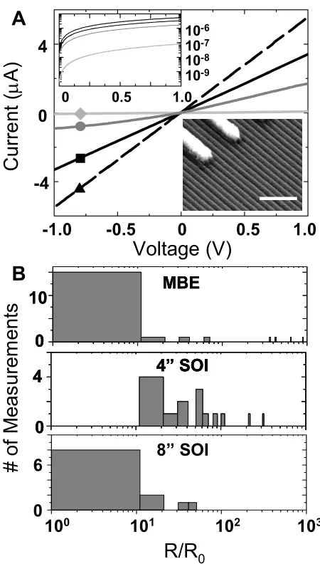
Figure 2-5.A (filled circle) shows a current-voltage (I-V) trace for a 7-μm-long section of Si NWs fabricated from the MBE substrate (30 nm of Boron:Si on intrinsic Si,
p = 1×1019 cm–3); the linearity of the trace confirms the ohmic nature of the contacts.
The histogram in Figure 2-5.B represents many such resistance measurements normalized
by the bulk-scaled resistance, Ro, and reveals the bulk-like conductivity of these NWs
despite their narrow width of ~10 nm. The good morphological properties of these NWs
apparently correspond to good electronic properties, confirming that the RIE recipe
described above does not damage the NWs.
In contrast, when Si NWs were fabricated from the same substrate used in
previou
se defects36, but for NWs of narrow width
(~10 nm here) even a small number of doping-induced defects can dramatically affect s studies10 (ion-implantation doped 4-inch SOI wafer; 25 nm of boron-doped Si
on 150 nm of SiO2; p = 3×1019 cm–3), the R/Ro histogram was centered at 104 (not
shown), indicating that the electrical properties of those NWs were severely degraded.
The most probable cause is lattice defects from ion-implantation methods.
Ion-implantation doping uses a high-energy beam of ionized dopant atoms to implant dopants
into the Si substrate. These high-energy dopants collide with Si atoms in the lattice and
produce point defects that degrade the conductivity of the substrate. Post-implantation
A
B
0
8” SOI 6
100 101 102 103
R/R
0# of
Meas
urem
ents
0 10 MBE 0 0 10 MBE4 4” SOI
0
4 4” SOI
4 4” SOI
Voltage (V)
0 4 -4C
rre
μ
0 0.5 1.01010-8 10-7
0 0.5 1.0
-0.5 -1.0
u
nt (
A)
-9 10-6Figure 2-5. Si nanowire electrical properties. A. IV measurements of 4 nanowire samples (all samples doped via spin-on diffusion doping): ■
8” SOI, p=5e19cm–3, 10nm×31nm×3μm ▲ 8”
SOI, n=1e20cm–3, 10nm×31nm×3μm ● MBE,
p=1e19cm–3, 10nm×30nm×7μm ♦ 4” SOI,
p=5e18cm–3, 10nm×25nm×2.5μm. Upper-left
inset shows data plotted on a semi-log scale. Lower-right inset shows an SEM image of the nanowire contacts; scale bar is 200 nm. B. Statistical distribution of normalized nanowire resistance (R/Ro) for various substrates. R/Ro
values for ion-implantation doped Si NWs are greater than 103 and are not shown. The bin size
is 10.
on doping to improve NW
conductivity, we used SNAP to
fabricate Si NWs from a 4-inch SOI
substrate doped with the spin-on
doping technique (25 nm of Si on
150 nm of SiO2, p = 5×1018 cm–3).
Figure 2-5.A (filled diamond) shows NW conductivity. This is confirmed
by the observation that we could
reliably fabricate conductive NWs
from ion-implanted substrates down
to 50 nm in width, but NWs of 10–
15 nm in width were frequently poor
conductors. Consequently, we
moved to spin-on doping as an
alternative to ion-implantation
doping. This method forgoes the use
of ion-implantation and instead uses
high-temperature annealing to gently
diffuse dopant atoms into the Si
lattice from a spin-on dopant source.
[image:40.612.116.341.71.467.2]spin-Figure 2-5.B shows a histogram
e
normalized resistance is still a factor of ten higher
fabricated from spin-on doped substrates are a th
their ion-implantation doped counterparts. This dra
the result of eliminating lattice defects from ion-im
importance of spin-on doping for the fabrication of c
Improving NW conductivity by another fac
scaled NW resistance, was accomplished simply
wafer as the starting material (8-inch industry-sta
Figure 2-5.A (filled square) shows a typical I-V sca doped 8-inch SOI wafer (30.8 nm of Si on 145 nm o
and Figure 2-5.B, the normalized resistance, wh
histogram of NWs fabricated from the MBE
fabricated from 8-inch spin-on doped SOI (30.8 nm
n = 1×1020 cm–3) also show bulk-scaled resistanc
typical I-V scan is showed in Figure 2-5.A (filled tri The SNAP technique was additionally used
a (111) surface orientation from bonded silico
Semiconductor, Vancouver, WA.; 40 nm of Si on
an I-V scan* for a 3-μm-long section of these NWs, and
of the normalized resistance constructed from s veral such I-V scans. Although the than the bulk-scaled resistance, NWs
ousand-times-better conductors than
matic increase in NW conductivity is
plantation doping, and highlights the
onductive NWs with narrow widths.
tor of ten, and thus achieving
bulk-by using a lower-defect-density SOI
ndard SOI† instead of 4-inch SOI).
n for NWs fabricated from a spin-on
f SiO2, 3-μm long, p = 5×1019 cm–3);
ich is comparable to the resistance
substrate. Phosphorous-doped NWs
of Si on 150 nm of SiO2, 3-μm long,
e (statistical data not shown) and a
angle, dashed line).
to fabricate high-quality Si NWs with
n(111)-on-insulator wafers (Isonics
2 μm of SiO2). In accord with the
* A slight non-linearity in the IV scan at voltages below 250 mV is observed, but length-dependent
resistance measurements revealed linear (ohmic) scaling implying that the observed resistance is dominated by the native NW conductivity and not by the contacts.
s from † Further confirmation of the superior quality of 8-inch industry standard SOI over 4-inch SOI come
0 1 2 3 4 5 6 7 8 0 2 3 4 1 5 6 Frequency R/Ro
Figure 2-6. Electrical properties of Si(111) nanowires. A. Representative current-voltage scans from 6 sets of Si(111) nanowires showing linear response and high conductivity. The top-left inset shows the same data plotted on a semi-log scale and the bottom-right inset shows a nanowire contact. B. Statistical distribution of normalized nanowire resistances (R/Ro). The bin size is 0.25. The inset shows a
zoomed-in SEM image of 15-nm wide
A
B
nanowires within a 150-element Si NW array. The scale bar is 200 nm.
200 nm
0 100 200 10 -7 10-6 10-4 10-5
Voltage (mV)
-200 -100 0 100 200 0 -100 -50 50 100 Cur ent ( A) r μ Voltage (mV) 200 nm
nm thick as received, but was thinned
to 40 nm through sacrificial dry
thermal oxidation and BOE wet
etching. The wafer was then diffusion
doped with phosphorus using the
spin-on doping method (n = 1×1020 cm–3),
and the SNAP technique was used to
fabricate 150-element arrays of
Si(111) NWs on top of an insulating
oxide (Figure 2-6.B
versatility of the SNAP technique, no modification was required to the procedures that
were described above in the context of (100) SOI wafers. The (111) SOI epilayer was 80-
, inset). The Si
shows a histogram of the normalized
resistance constructed from several
such I-V scans.
By comparing the normalized
NW resistance histograms of Figures NWs were sectioned into regions 1
μm in length, then contacted and
tested as described above. Figure
2-6.A shows representative I-V scans from these NWs and Figure 2-6.B
i
effects that ion-implantation processes have on S
layer of the (100) SOI wafers used in the study ab
the separation by implanted oxygen (SIMOX) tec implantation doping in that it bombards the silic
ions. Oxygen ions are implanted into the Si su
separating the Si epilayer from the substrate. L
implantation anneal does not repair all of the
epilayer. In contrast, the (111) SOI wafers were fabricated (commercially) using a
bonding technique whereby two oxidized Si waf
lantation.
fabricated from the (111)-oriented SOI substrates are better conductors than those
fabricated from (100)-oriented SOI substrates. (The R/Ro distribution for the Si(111)
des further evidence of the detrimental
i NW conductivity. The buried oxide
ove were created (commercially) using
hnique. This process is similar to
ion-on surface with an energetic beam of
bstrate to form a buried SiO2 layer
ike ion-implantation doping, a
post-implantation-related defects in the Si
ers are bonded together at their SiO2
surfaces, thus forming a SOI
structure without the need for
oxygen ion imp NWs is more sharply peaked at unity.) This prov
Using NWs fabricated from a
4-inch spin-on doped SOI substrate
(7.5-μm long, p = 5×1018 cm–3), a
crossbar-FET was constructed by
depositing 7 nm of Al2O3 over the
NW array, followed by a
250-nm-wide metallic wire as a gate. Figure
2-7 shows the gating response for
Figure 2-7. P-type nanowire gating responsefor various values of the source-drain voltage. The asymmetry in source-drain bias is attributed to asymmetrical Schottky barriers.
-1.0 -0.5 0.0 0.5 1.0
-10 0 10 20
Cur
rent (nA)
V
Gate(V)
+ 1.0 V + 0.5 V + 0.1 V - 0.1 V - 0.5 V - 1.0 V
various values of the source-drain voltage. An impressive modulation in conductivity was
obtained through a gate bias of just ±1V. (Although difficult to see in the figure, we could
tune the NW conductivity by a factor of 103.) These results show that by minimizing
defects at all stages of NW fabrication we can fabricate Si NWs with bulk-scaled
conductance that are highly responsive to field-effect gating.
2.4 Silicon nanowire doping
The observation that diffusion-doped Si NWs are thousand-fold-better conductors than
iffusion doping an important part of
s, I will discuss the technical aspects
SNAP NW fabrication. their ion-implantation-doped counterparts makes d
w
of diffusion doping using spin-on dopants for use in
Most spin-on dopants consist of the desired dopant s
boron) incorporated into a SiO2 polymer-matrix and
dopant solution is spin-coated onto a clean Si
temperature to drive off solvent. This results in the
film on the Si surface that provides a virtually infin
is then annealed at high temperature in an inert e
dopant atoms from the dopant-rich SiO2 film into t
simple and gentle route for doping SOI epilayers tha
the dopant, annealing and removing the dopant. Because spin-on doping requires high the SNAP NW fabrication protocol. In what follo
pecies (such as phosphorus or
dissolved in an organic solvent. This
chip and baked at an intermediate
formation of a thin, dopant-rich SiO2
ite source of dopant atoms. The chip
nvironment to facilitate diffusion of
he Si lattice. This method provides a
t is compatible with batch-processing
for manufacturability.
![Figure 1-2. A false-colored scanning electron micrograph of a molecular electronic memory circuit fabricated from [2]rotaxane molecular materials and SNAP-fabricated silicon and titanium nanowires](https://thumb-us.123doks.com/thumbv2/123dok_us/8816917.920721/20.612.143.504.78.329/micrograph-molecular-electronic-fabricated-molecular-materials-fabricated-nanowires.webp)