N A N O E X P R E S S
Open Access
The current image of single SnO
2
nanobelt
nanodevice studied by conductive atomic force
microscopy
Shujie Wang, Gang Cheng, Ke Cheng, Xiaohong Jiang and Zuliang Du
*Abstract
A single SnO2 nanobelt was assembled on a pair of Au electrodes by electric-field assembly method. The
electronic transport property of single SnO2nanobelt was studied by conductive atomic force microscopy (C-AFM). Back-to-back Schottky barrier-type junctions were created between AFM tip/SnO2 nanobelt/Au electrode which can be concluded from the I-V curve. The current images of single SnO2 nanobelt nanodevices were also studied by C-AFM techniques, which showed stripes patterns on the nanobelt surface. The current images of the nanobelt devices correlate the microscopy with separate transport properties measurement together.
Keywords:SnO2 nanobelt, C-AFM, current image
Introduction
As an important wide band n-type semiconductor, SnO2
possesses many unique optical and electrical properties which have been widely used in optoelectronic devices and gas sensors [1-4]. One dimensional (1-D) SnO2
have been reported to have some different characteris-tics from the bulk crystal due to its large surface-to-volume ratio [5]. Nanodevices based on 1-D SnO2
nanostructures have been fabricated and showed signifi-cant potential for applications ranging from field-effect transistors, gas sensors, displays, as well as solar cells [6-9]. Although promising results of the gas sensing and other performance of 1-D SnO2 have been reported, the
development of highly sensitized devices remains a future challenge. Usually, the surface atoms and states on the (1-D) SnO2 surface play an important role in its
transport behavior which complicates the nanodevice characterization [10]. Recent research result showed that the surface states indeed existed in these wires which could be detected in a contactless manner by spectral analysis [11]. Thus the better understanding of the sur-face states affected the device transport property needed. The transport property of the nanobelts device and the surface states on the (1-D) SnO2 surface must be cared
in order to fabricate the practical application of nanode-vices. It is difficult for us investigating the transport property of one single nanobelt in the nanometer scale before atomic force microscopy (AFM), especially the conductive AFM (C-AFM) with a conductive tip; in recent years, more and more are used to investigate the transport property and the surface property on the nanostructure in microscope scales [12-15]. AFM tip coated with metal can serve as the conducting electrode, and the transport property of the nanowires can be stu-died through the I-V curve recorded by C-AFM
techni-que [16]. Furthermore, the current image,
simultaneously with the AFM topography, can provide the direct information how the current flows through the nanostructure surface [17,18]. In this paper, singe SnO2nanobelt device is assembled across opposing Au
electrodes by electric-field assembly method [19]. Non-linear and asymmetric I-V curve are obtained by apply-ing a small voltage onto the conductive AFM tip positioned directly on the surface of SnO2 nanobelt. We
conclude the nonlinear and asymmetric I-V behavior resulted from the back-to-back Schottky barriers between AFM tip/SnO2 nanobelt/electrode, and the
Schottky barriers is related to the surface states on the nanobelt surface. The current images of the nanobelt device are also studied by C-AFM techniques, which show the current flow through the single nanobelt
* Correspondence: [email protected]
Key Laboratory for Special Functional Materials, Henan University, Kaifeng 475004, People’s Republic of China
devices clearly. The results showed that the surface states can affect the transport property of the nanobelt device and display stripe patterns in the current images.
Experiment
SnO2 nanobelts are synthesized using techniques
described in Ref. [20]. Briefly, a horizontal alumina tube (outer diameter, 3.7 mm; length, 120 cm) is mounted inside a high-temperature tube furnace. A mixture of SnO2 and graphite powders is placed on an alumina
wafer. After transferring the wafer to the center of the alumina tube, the tube is evacuated by a mechanical rotary pump to a pressure of 6 × 10⁻²Torr. During the experiment, a constant flow of N2 is maintained, and
the pump continually evacuated the system to keep the pressure inside the tube. The temperature of the furnace is increased to 900°C from room temperature and kept at 900°C for 1 h. After the furnace is cooled down to room temperature, a white wool-like product is formed in a high yield on Si wafer near the boat of the wafer.
In order to fabricate one single SnO2nanobelt
nano-device, the nanobelts are assembled on a pair of Au electrodes by electric-field assembly method [21]. The SnO2 nanobelts were ultrasonically dispersed in ethanol,
and then the dispersed SnO2 nanobelts were deposited
on predefined Au electrodes using the electric-field assembly technique. After applying a droplet of the SnO2 nanobelt suspension onto the electrodes, the
elec-trodes were connected to a 10 V and 50-kHz AC signal, which was chosen for optimizing the alignment of a sin-gle nanobelt. This signal generated an alternating elec-trostatic force on the nanobelts in the solution. Under the electrical polarization force, the nanobelts were deposited on the electrodes.
Results and discussion
A typical scanning electron microscopy (SEM) image of Figure 1a shows that the as-synthesized products consist of nanometer belt-like structures. Figure 1b shows the
SEM image of the assembled nanobelt which confirms that only one single nanobelt is assembled on the Au electrode pair.
Figure 2a is transmission electron microscopy (TEM) image of a single SnO2 nanobelt. High-resolution
trans-mission electron microscopy (HRTEM) image of a single SnO2 nanobelt is obtained with a JEM-2010
transmis-sion electron microscope (Figure 2b). It shows a single nanobelt with diameter of about 40 nm. And well-defined lattice fringe separation with 0.33 nm corre-sponding to (110) planes of SnO2. It is also in
agree-ment with the selected area electron diffraction results (the inset of Figure 2b).
The electronic transport property of SnO2nanobelt is
carried out by C-AFM techniques with Au-coated sili-con tip. Figure 3a is the measurement setup diagrams in our experiment. In the current-voltage (I-V) measure-ments, a metal/semiconductor point contact will be formed by placing the Au-coated conductive tip on SnO2 nanobelt top surface. And another end of the
nanobelt is contact with the metal electrode, so the metal-semiconductor-metal (M-S-M) structure is formed. When a voltage bias (from +6.0 to -6.0 V) is added on the Au tip, a clearly nonlinear and asymmetric I-V curve is obtained as shown in Figure 3b.
The electronic transport properties of SnO2 nanowires
have been studied by F. Hernandez-Ramirez in contact with Pt metal electrode [22]. The nonlinear I-V curve is attributed to the back-to-back Schottky barrier-type junctions formed between the nanowire and the metal electrode. Here, the C-AFM tip serves as one end of the electrode, and another end is the Au electrode, so the back-to-back Schottky barrier structure in series with the resistance of SnO2nanobelt is formed. In this
[image:2.595.56.539.580.712.2]struc-ture, the current is dominated by the reverse current of reverse-biased Schottky barrier. The I-V curves in our experiment at different bias voltage are all the reverse current of the Schottky diode. Our analysis of the reverse-biased Schottky barrier is based on the
Figure 1SEM images of SnO2nanobelt. (a) SEM images of SnO2nanobelt. (b) SEM image of a single SnO2nanobelt across the Au electrodes.
Wanget al.Nanoscale Research Letters2011,6:541 http://www.nanoscalereslett.com/content/6/1/541
Figure 2TEM image of SnO2nanobelt. (a) TEM image of SnO2nanobelt. (b) HRTEM of single SnO2nanobelt. An inset image of (b) is
diffraction pattern of SnO2nanobelt.
Figure 3AFM measurement. (a) C-AFM measurement setup. (b) I-V curve measured by conductive AFM tip on the top of SnO2nanobelt top
[image:3.595.60.539.297.674.2]thermionic-field emission model of Padovani and Strat-ton [23]. Tunneling through the reverse-biased Schottky barrier becomes significant in the nano-M-S-M struc-ture. And the tunneling current is mainly the thermio-nic-field emission current and the current density through the reverse-biased Schottky barrier is given by:
lnI= ln(SJ) = ln(SJs) +V(
q kBT −
1
E0) (1)
where Sis the contact area associated with Schottky barrier,J is the current density through Schottky barrier,
Vis the applied revere bias, q is the unit charge of an electron, KBis the Boltzmann’s constant, E0 is a para-meter that depends on the carriers’density,Jsis a slowly varying function of applied bias. Equation 1 indicates that the logarithmic of the current is linear with reverse bias. The log-scale plots of positive and negative current are shown in Figure 3c. We can see that lnIis linear with Vin the intermediate bias range for both positive and negative current, which shows the typical I-V char-acteristic of back-to-back Schottky barriers structure. We can also find that in Eq. (1), the current value is related to contact area of the Schottky barrier. For the contact area of Au tip and SnO2, it is much smaller
than the metal electrode due to the nanometer scale resolving of the AFM tip, which may be the main reason for the asymmetric I-V curve made on the nanobelt sur-face. Therefore the nonlinear and rectifying behavior in our I-V curve resulted from the Schottky contact between AFM tip/SnO2 nanobelt/electrode and the
Schottky barriers may be related to the surface states on the nanobelt surface.
In order to illustrate and how the surface states affect the transport property of single SnO2 nanobelt clearly,
current maps are carried out by C-AFM at negative bias voltage. The negative bias voltage here is consistent with the bias voltage at the I-V curve record on the SnO2
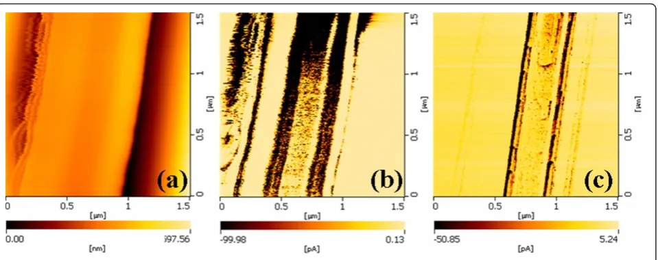
nanobelt. The voltage value (we selected -4.0 V) should be larger than 2.0 according to the I-V curves we made on the nanobelt surface. Here, current maps can provide direct transport property information on the surface of the nanobelt. It correlates the microscopy with separate device transport measurement together which can intro-duce us the device property of the nanobelt in nan-ometer scales [24]. Figure 4 is the topography and current images of single SnO2 nanobelt between the
gaps of the metal electrode. The scan area is 1.5 × 1.5
μm, which is smaller than the gap of the electrode (5
μm). At -4.0-V bias voltages, the current maps are almost identical to that of surface geography (Figure 4a, b). In the contrast of the current images, dark and bright spots indicate relatively low and high values of the current flow through the SnO2 nanobelt. According
to Figure 4, the current image show stripe patterns on the nanobelt surface which indicate the conducting channels of the current through the nanobelt surface. The current maps show us that the much larger current appeared at the edge and on specific area of the SnO2
nanobelt. From the surface geography of Figure 4a, we find that the edge of the SnO2nanobelt is irregular and
also there are height variations on the specific area on the surface of SnO2nanobelt. And these irregular
struc-tures which are caused from the nanobelt preparation process are correlative with the stripe pattern current images of the SnO2 nanobelt. At the same time the
sur-face states are formed on these defect areas due to greater number of oxygen vacancies on it.
We have demonstrated that the Schottky barriers between CuO nanowires and metallic electrodes are dominated by the surface states on the semiconductor nanowires surface, and the conductive atomic force microscopy current maps showed the current varied with the surface states of the nanowire [25]. Thus the surface states are widely existing phenomena for semi-conductor nanobelts or nanowires. Here, the SnO2
nanobelts have some defect areas in its preparation pro-cess. So oxygen vacancies and the defect on the nano-belt would serve as surface states and impact the transport property of the nanobelt. According to the I-V curves analysis above, Schottky barrier junction is formed between the tip of AFM and the nanobelt sur-face. In this structure, the current is dominated by the tunneling current of reverse-biased Schottky barrier. And the tunneling current is dominated by the surface states on the nanobelt surface. That is to say, the cur-rent images of the SnO2nanobelt is caused by the
sur-face states which result from the oxygen vacancies and the defect on the nanobelt that we can analyze from the surface geography of Figure 4a. Thus the low- and high-current flow through the nanobelt will happened and can be visualized as stripe patterns in our current maps. Through the second scan of the same area under the same bias, lowered current images are obtained. The large current is decreased with repeated scan at the same area on the nanobelt surface just as Figure 4c showed. In C-AFM scans, the bias voltage is applied on the nanobelt surface, and electron is injected from the AFM tip through the depletion layer into the nanobelt. Here, the surface states tend to trap electrons further and widen the depletion layer which leads to the decrease in electron mobility as well as a decrease in the current value in the same area on the nanobelt surface. The surface states trap charge carriers in the first scan of C-AFM at -4.0 bias voltages and enhance the barrier height on the nanobelt surface, when the same bias vol-tage is add on the nanobelt again decreased currents image will be obtained.
Wanget al.Nanoscale Research Letters2011,6:541 http://www.nanoscalereslett.com/content/6/1/541
The photocurrent maps are also carried out at the same bias voltage values by our photo-assisted AFM techniques with an UV light source (l= 350 nm, aver-age power of 8 mW) [14], but the current values have no obvious changes, the varied value only are several picoamperes. The surface states tend to extract electrons from SnO2 which can form a depletion of the charge
carriers in the nanobelt. The depletion layer which is caused by the surface states can affect the conducting property of the nanobelt. Also, the depletion regions in the nanobelt can act as obstacles that hinder the elec-tron transfer from the nanobelt to the electrode and increase the turn-on voltage of the nanobelt devices. Usually, the surface states can be modified by the excit-ing UV light. The UV photons can release of the trapped electrons back into the depletion region, gradu-ally reducing the band bending. Since the nanobelts have a greater number of oxygen vacancies, the deple-tion region and surface field is larger, the effect of UV light is not as strong as make photocurrent changes in our current images. Surface states as the charge trapping effect in nanometer scale must be cared in nano-electro-nic device fabricated in the future. Thus, the electronano-electro-nic transport property of single nanobelt nanodevices is directly studied by correlating the microscopy with sepa-rate device measurement together. Current maps show us clearly the transport property of the nanobelt at nan-ometer scales.
Conclusion
In conclusion, the electronic transport property of single SnO2 nanobelt was studied by conductive atomic force
microscopy (C-AFM). Back-to-back Schottky barrier-type junctions were created between AFM tip/SnO2
nanobelt/electrode which reasoning from the I-V curve made on the nanobelt. The current images of single SnO2 nanobelt nanodevices were also studied by
C-AFM techniques, which showed stripes patterns on the nanobelt surface. The results showed that the surface states can affect the transport property of the nanobelt device and display stripe patterns in the current images. The electronic transport property of single SnO2
nano-devices affect by the surface states can be important for constructing nanosensors and other nanodevices based on SnO2nanobelt in nanometer scales in future.
Acknowledgements
This work was supported by the National Natural Science Foundation of China (Grant No. 10874040, 60906056), and the Cultivation Fund of the Key Scientific and Technical Innovation Project, Ministry of Education of China (No. 708062). Fund of Science and Technology Department (No. 102300413223) and Education department (No. 2009A140001) of Henan Province.
Authors’contributions
WSJ is the primary author and carried out the experiments, characterization, and acquisition of data. CG participated in analysis and interpretation of data. CK and JXH participated in language modification. ZLD is the principal investigator helped analysis and interpretation of data, drafting of the manuscript and revisions. All authors read and approved the final manuscript.
Competing interests
The authors declare that they have no competing interests.
Received: 21 July 2011 Accepted: 4 October 2011 Published: 4 October 2011
References
1. Korotcenkov G, Han SD, Cho BK, Brinzari V:Grain size effects in sensor response of nanostructured SnO2-and In2O3-based conductometric thin
[image:5.595.60.540.87.277.2]film gas sensor.Crit Rev Solid State Mater Sci2009,34:1-17.
Figure 4Current images of SnO2nanobelt. (a) Surface topography, (b) current maps at -4.0 V, (c) reduced current images in the second scan
2. Gurlo A:Nanosensors: towards morphological control of gas sensing activity. SnO2, In2O3, ZnO and WO3case studies.Nanoscale2011,
3:154-165.
3. Bueno PR, Varela JA, Longo E:SnO2, ZnO and related polycrystalline
compound semiconductors: an overview and review on the voltage-dependent resistance (non-ohmic) feature.J Eur Ceram Soc2008, 28:505-529.
4. Batzill M:Surface science studies of gas sensing materials: SnO2.Sensors
2006,6:1345-1366.
5. Pan ZW, Dai ZR, Wang ZL:Nanobelts of semiconducting oxides.Science
2001,291:1947-1949.
6. Dai ZR, Gole JL, Stout JD, Wang ZL:Tin oxide nanowires, nanoribbons, and nanotubes.J Phys Chem B2002,106:1274-1279.
7. Li QH, Chen YJ, Wan Q, Wang TH:Thin film transistors fabricated byin
situgrowth of SnO2nanobelts on Au/Pt electrodes.Appl Phys Lett2004,
85:1805-807.
8. Ji X, Huang X, Liu J, Jiang J, Li X, Ding R, Hu Y, Wu F, Li Q:Carbon-coated SnO2nanorod array for lithium-ion battery anode material.Nanoscale Res Lett2010,5:649-653.
9. Han JH, Yoon DY:3D CFD for chemical transport profiles in a rotating disk CVD reactor.3D Research2010,02:26-30.
10. Kar A, Stroscio MA, Dutta M, Kumari J, Meyyappan M:Observation of ultraviolet emission and effect of surface states on the luminescence from tin oxide nanowires.Appl Phys Lett2009,94:101905.
11. Chen HT, Xiong SJ, Wu XL, Zhu J, Shen JC:Tin oxide nanoribbons with vacancy structures in luminescence-sensitive oxygen sensing.Nano Lett
2009,9:1926-1931.
12. Yaish Y, Park JY, Rosenblatt S, Sazonova V, Brink M, McEuen PL:Electrical nanoprobing of semiconducting carbon nanotubes using an atomic force microscope.Phys Rev Lett2004,92:046401.
13. Tanaka I, Kamiya I, Sakaki H, Qureshi N, Allen SJ Jr, Petroff PM:Imaging and probing electronic properties of self-assembled InAs quantum dots by atomic force microscopy with conductive tip.Appl Phys Lett1999,74:6. 14. Wang SJ, Zhang XT, Cheng G, Jiang XH, Li YC, Huang YB, Du Z:Study on
electronic transport properties of WO3/TiO2nanocrystalline thin films by
photoassisted conductive atomic force microscopy.Chem Phys Lett2005, 405:63-67.
15. Fiorenza P, Nigro RL, Raineri V:Scanning probe microscopy on heterogeneous CaCu3Ti4O12thin films.Nanoscale Res Lett2011,6:118.
16. Pérez-García B, Zúñiga-Pérez J, Muñoz-Sanjosé V, Colchero J, Palacios-Lidón E:Formation and rupture of Schottky nanocontacts on ZnO nanocolumns.Nano Lett2007,7:1505.
17. Azulay D, Millo O, Silbert S, Balberg I, Naghavi N:Where does
photocurrent flow in polycrystalline CdS?Appl Phys Lett2005,86:212102. 18. Zhang L, Mitani Y:Structural and electrical evolution of gate dielectric
breakdown observed by conductive atomic force microscopy.Appl Phys Lett2006,88:032906.
19. Liu YL, Chung JH, Liu WK, Ruoff RS:Dielectrophoretic assembly of nanowires.J Phys Chem B2006,110:14098-14106.
20. Hu JQ, Ma XL, Shang NG, Xie ZY, Wong NB, Lee CS, Lee ST:Large-scale rapid oxidation synthesis of SnO2 nanoribbons.J Phys Chem B2002, 106:3823-3826.
21. Chen Z, Yang YL, Chen F, Qing Q, Wu ZY, Liu ZF:Controllable interconnection of single-walled carbon nanotubes under AC electric field.J Phys Chem B2005,109:11420-11423.
22. Hernandez-Ramirez F, Tarancon A, Casals O, Pellicer E, Rodriguez J, Romano-Rodriguez A, Morante JR, Barth S, Mathur S:Electrical properties of individual tin oxide nanowires contacted to platinum electrodes.Phys Rev B2007,76:085429.
23. Padovani FA, Stratton R:Field and thermionic-field emission in Schottky barriers.Solid-State Electron1966,9:695-707.
24. Stratakis E, Misra N, Spanakis E, Hwang DJ, Grigoropoulos CP, Fotakis C, Tzanetakis P:Imaging dielectric properties of Si nanowire oxide with conductive atomic force microscopy complemented with femtosecond laser illumination.Nano Lett2008,8:1949-1953.
25. Cheng G, Wang SJ, Cheng K, Jiang XH, Wang LX, Li LS, Du ZL, Zou GT:The current image of a single CuO nanowire studied by conductive atomic force microscopy.Appl Phys Lett2008,92:223116.
doi:10.1186/1556-276X-6-541
Cite this article as:Wanget al.:The current image of single SnO2 nanobelt nanodevice studied by conductive atomic force microscopy.
Nanoscale Research Letters20116:541.
Submit your manuscript to a
journal and benefi t from:
7Convenient online submission 7Rigorous peer review
7Immediate publication on acceptance 7Open access: articles freely available online 7High visibility within the fi eld
7Retaining the copyright to your article
Submit your next manuscript at 7 springeropen.com
Wanget al.Nanoscale Research Letters2011,6:541 http://www.nanoscalereslett.com/content/6/1/541