N A N O E X P R E S S
Open Access
Effect of Surface Scattering of Electrons on
Ratios of Optical Absorption and Scattering
to Extinction of Gold Nanoshell
Yiyang Ye
1*, T. P. Chen
1*, Zhen Liu
2and Xu Yuan
3Abstract
Gold nanoshell’s high light scattering and absorption at its resonance wavelength have found applications in biomedical imaging and photothermal therapy. However, at nanoscale, metallic material’s dielectric function is affected by nanoparticle’s size, mainly via a mechanism called surface scattering of conduction electrons. In this work, the effect of surface scattering of electrons on the ratios of optical absorption and scattering to extinction (which is the sum of the absorption and scattering) of gold nanoshell is investigated. Simulation results for several shell thicknesses are compared. It is found that the electrons’surface scattering increases the optical absorption ratio, and the thinner the shell thickness, the larger the increase in the difference of the absorption ratio between the situations with and without the surface scattering considered. The increase of absorption ratio is then verified by comparing simulation results to experimental measurements for three nanoshells. The parameters of the simulations to fit the experimental measurements show that the damping of conduction electrons in metallic shell geometry is larger than that predicted by the billiard scattering model.
Keywords:Nanoshell, Surface scattering, Light absorption, Light scattering
Background
Gold nanoshell is composed of a dielectric core, which may be silica orAu2S[1,2], and a concentric shell of gold. Due to gold’s biocompatibility [3, 4], facile conjugation of anti-bodies and targeting moieties to gold shell’s surface [5], tun-ability of its resonant wavelength to the near infrared region [2,6], and a region called the biological water win-dow where the tissue transmissivity is the highest [7], gold nanoshell’s enhanced light scattering and absorption have found applications in biomedical imaging and photother-mal therapy [8, 9]. Mie theory’s extension for core-shell structure can be employed to calculate a single gold nano-shell’s optical absorption and scattering cross sections [10], and the sum of these two gives its extinction cross section. Since the thickness of gold nanoshell is usually smaller than or comparable to electron’s mean free path in bulk gold, which is about 37.7 nm [11], electrons in gold shell go through more collisions per unit time (extra collisions
caused by scattering of conduction electrons from shell sur-face) than they do in bulk gold [12,13]. Surface scattering of conduction electrons has been reported to cause broad-ening of resonance peak, which was verified by fitting of measured and calculated spectra [6,14–16], and reduction in the absolute values of both scattering and absorption of a single nanoshell which was demonstrated by theoretical calculations [17–19]. However, for scattering-based bio-medical imaging applications [9, 20, 21], where metallic nanoparticles or fluorescent materials are attached to target tissue or cells, if it is desired to only image and not ther-mally damage the tissue or cells under investigation, it is important that the attached nanoparticle has high ratio in scattering and low ratio in absorption at the desired wave-length. The reason why ratios of scattering and absorption but not their absolute values are of concern is that decrease in absolute values of scattering and absorption can be com-pensated by having more particles attached to the target tis-sue or cells. Application of metallic nanoparticle’s resonant light scattering in transparent projection screen [22–25], and in photovoltaics [26–30], also requires simultaneous high scattering and low absorption ratios at the desired * Correspondence:[email protected];[email protected]
1School of Electrical and Electronic Engineering, Nanyang Technological
University, Singapore 639798, Singapore
Full list of author information is available at the end of the article
© The Author(s). 2018Open AccessThis article is distributed under the terms of the Creative Commons Attribution 4.0 International License (http://creativecommons.org/licenses/by/4.0/), which permits unrestricted use, distribution, and reproduction in any medium, provided you give appropriate credit to the original author(s) and the source, provide a link to the Creative Commons license, and indicate if changes were made.
Yeet al. Nanoscale Research Letters (2018) 13:299
wavelength range. What is more, gold metamaterials also require gold to be of the form of thin film, which can achieve high optical absorption as light absorber [31,32], or high transmittance as transparent conducting film [33–36], and thus, conduction electrons’ surface scattering effect plays a role too. Therefore, it may give some guidance on designing nanoscale gold-related structure to investigate the effect of surface scattering of electrons on the ratios of optical absorption and scattering to extinction for gold nanoshells.
In this work, simulations are first conducted to study the effect of surface scattering of electrons on the ratios of optical absorption and scattering to extinction of gold nanoshells by considering the situations with and with-out the surface scattering. It is shown that the electrons’ surface scattering increases the optical absorption ratio and therefore decreases the light scattering ratio, and the thinner the shell thickness, the larger the increase in the optical absorption ratio. The increased absorption is then verified experimentally for three samples by com-paring their measured and simulated absorption as well as extinction spectra.
The simulation and experimental results will be shown first in the “Results and Discussion” section, and then, detailed method of optical measurements of extinction and absorption is provided in the“Methods/Experimental” section, to avoid unnecessary confusion caused by the descriptions of optical measurements.
Results and Discussion
Gold nanoshells with four different shell thicknesses but same core diameter are studied by simulation. The gold nanoshells include (80-nm-diameter silica core)@(15-nm-thick gold shell), (80-nm-diameter sil-ica core)@(25-nm-thick gold shell), (80-nm-diameter silica core)@(35-nm-thick gold shell), and (80-nm-dia-meter silica core)@(45-nm-thick gold shell).
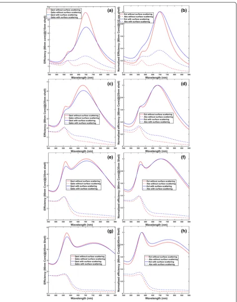
After interaction of parallel incident rays of light with a single nanoparticle, apart from those directly transmit-ted (propagating in the original direction of the incident light), light is either absorbed or scattered, and the sum of these two is referred to as extinction [37]. The scatter-ing, absorption, and extinction, quantized in terms of cross sections, which can be intuitively perceived as the area amount of light removed from the path of incident light due to scattering, absorption, or extinction respect-ively, can be calculated by Mie theory’s extension for core-shell structure [10]. However, it is more natural to normalize the cross sections to the nanoparticle’s geo-metric cross section,πR2, where Ris the outer radius of a core-shell structure, for the purpose of comparison between different structures, and the ratio of j cross section (j=absorption, scattering, or extinction) to the geometric cross section is termed asjefficiency.
The extinction and absorption efficiencies without consideration of surface scattering effect are calculated by using bulk gold’s dielectric function [38] as input to the Mie theory, and they are shown as red lines (solid or dashed) in Fig.1. To take into account the effect of sur-face scattering, it is assumed that the dielectric function of gold has a Drude model component to describe the behavior of free electrons [39], and an extra damping term γs contributed by surface scattering of conduction
electrons is added to the bulk damping γbin the Drude
term to give the corrected dielectric functionεshfor gold
shell [19]:
εsh¼εexpþ
ω2 p
ω ωþiγb
− ω2p
ω ωþiðγbþγs
ð1Þ
where εexp is gold’s bulk dielectric function from refer-ence [38], ωp is the plasma frequency of gold, ω is the frequency of the incident light, and i is the imaginary number. For the calculated efficiencies with surface scat-tering effect in Fig. 1 (blue lines, solid, or dashed), ωp andγbare assumed to be 8.55 eV and 18.4 meV
respect-ively [19]. Andγsis given by [19]:
γs¼
vF
LB ð
2Þ
wherevFis the Fermi velocity of electrons in gold and is
equal to 1.40 × 10⁶m/s [19] andLBis the effective mean
free path of the electrons in the shell, derived by assum-ing billiard scatterassum-ing model [13], in which the reflec-tions of electrons from the two surfaces of shell are specular, and is given by
LB¼
4 r3 o−r3i
3 r2 oþr2i
ð3Þ
where ro and ri are the outer and inner radius of the
nanoshell respectively. The refractive indexes of the sur-rounding medium and silica core are assumed to be 1.5 and 1.45 respectively.
Fig. 1(See legend on next page.)
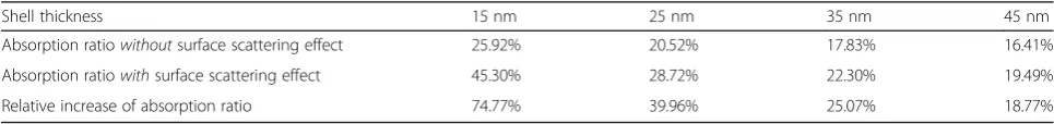
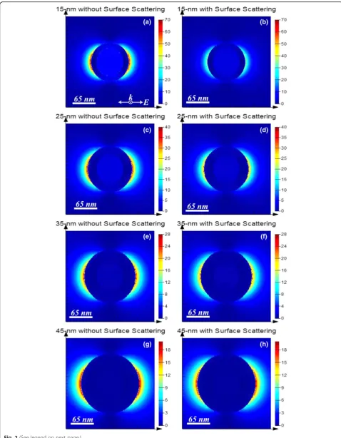
[image:3.595.61.540.84.695.2]positions. Intuitively, the increase in absorption ratio after considering surface scattering effect becomes less signifi-cant with increasing shell thickness, as can be observed in (b), (d), (f), and (h) in Fig.1. This is because the thicker the shell, the less the frequency of electrons’collisions with the shell surfaces, i.e., surface scattering effect is reduced. The phenomenon is also confirmed by Table1. For each shell thickness, the absorption ratio with (without) surface scat-tering, calculated by the ratio of the region under the blue (red) dashed curve to the region under the blue (red) solid curve, is tabulated in Table 1. To further investigate the mechanism behind the increase of absorption ratio, spatial distributions of square of near electric field amplitude |E|2 are plotted in Fig.2. In Fig.2, it can be observed that |E|2s
calculated without surface scattering are larger than those with surface scattering, which may be explained in this way: assuming surface scattering takes effect, conduction elec-trons experience more collisions from shell surfaces as com-pared to those in bulk gold, so conduction electrons’average oscillation amplitude is decreased, leading to reduced |E|2s. And since collisions of conduction electrons with shell sur-faces contribute to energy loss as heat, the absorption ratio is increased after including surface scattering effect.
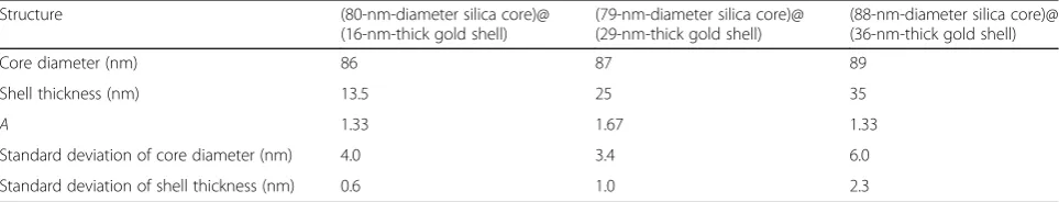
Subject to availability of material, absorption and extinc-tion are experimentally measured for three nanoshells of different shell thicknesses but similar core diameters: (80-nm-diameter silica core)@(16-nm-thick gold shell), (79-nm-diameter silica core)@(29-nm-thick gold shell), and (88-nm-diameter silica core)@(36-nm-thick gold shell), whose TEM images are shown in Fig. 3. Figure 4 shows the comparison between the experimentally mea-sured and theoretically simulated results for the three nanoshells. It can be observed in Fig.4that the calculated absorption cross sections with the surface scattering effect taken into account agree well with the measured results for all of the three nanoshells, while there is a large
departure between the measured and simulated absorp-tions if the surface scattering effect is not considered.
To fit the calculated extinctions (the solid blue lines) to the experimentally measured extinctions (the solid red lines), which are shown in Fig. 4, the expression of the extra dampingγsin Eq. (1) due to surface scattering
is given by Eq. (4) shown below [15], instead of Eq. (2).
γs¼
AvF
ds ð
4Þ
whereAis a dimensionless fitting parameter and a larger
A indicates a larger damping and ds is the shell
thick-ness. The fitting parameterAis affected by many factors: electron density at the surface, effect of the interface, an-isotropy of particle, and quantum mechanical computa-tion, and its value has been shown to range from 0.1 to above 2 [40,41]. Note that we can write Eq. (2) into the form of Eq. (4) to compare the theoretical value of A
predicted by billiard scattering model to those fitted from experiment, by first calculating the value of LB in
Eq. (2) using Eq. (3), and then writingLBin Eq. (2) into
the form ofds/A, as shown in Eq. (5a) to (5d) below:
γs¼
vF
LB¼vF∙
3 r2oþr2i
4 r3 o−r3i
ð5aÞ
write
3 r2 oþr2i
4 r3 o−r3i
¼ A
ds ð5bÞ
then
γs¼
AvF
ds ð5cÞ
where
(See figure on previous page.)
[image:4.595.303.538.482.639.2]Fig. 1Calculated extinction and absorption efficiencies with and without consideration of surface scattering of conduction electrons, whereQext (Ext) stands for extinction efficiency (normalized extinction) andQabs(Abs) stands for absorption efficiency (normalized absorption). The scattering efficiency (normalized scattering) is the difference between theQext(Ext) andQabs(Abs). All calculations are carried out by Mie theory, with silica and surrounding medium’s indices assumed to be 1.45 and 1.5 respectively. Gold’s dielectric constants without surface scattering are from reference [38], while those with surface scattering are given by Eqs. (1)~(3).aandbare for (80-nm-diameter silica core)@(15-nm-thick gold shell). canddare for (80-nm-diameter silica core)@(25-nm-thick gold shell).eandfare for (80-nm-diameter silica core)@(35-nm-thick gold shell).gand hare for (80-nm-diameter silica core)@(45-nm-thick gold shell). The left column, i.e.,a,c,e, andg, is the corresponding efficiencies as calculated by Mie theory. The right column, i.e.,b,d, andf, is the efficiencies normalized to the dipolar resonance peak (the resonance peak between 700 and 800 nm), andhthe efficiencies normalized to the quadrupolar resonance peak (the peak between 550 and 600 nm)
Table 1Comparison of the absorption ratio between the calculations with and without the surface scattering effect of conduction electrons. The results are obtained from Fig.1
Shell thickness 15 nm 25 nm 35 nm 45 nm
Absorption ratiowithoutsurface scattering effect 25.92% 20.52% 17.83% 16.41%
Absorption ratiowithsurface scattering effect 45.30% 28.72% 22.30% 19.49%
[image:4.595.56.539.675.732.2]Fig. 2(See legend on next page.)
[image:5.595.57.536.86.701.2]A¼ds∙ 3 r2
oþr2i
4 r3 o−r3i
ð5dÞ
Note that when the shell thickness is less than 25% of the total radius, Eq. (5d) gives an A value of about 0.5 [13]. The values of the fitting parameters for the calcu-lated spectrums of the three nanoshells shown in Fig.4 are tabulated in Table2.
The calculated extinction and absorption spectrums shown in Fig. 4, which are normalized to the dipolar peak, have considered the surface scattering and size dis-tribution. For each nanoshell, the standard deviations of the core diameter and shell thickness are computed re-spectively by multiplying the core diameter and shell thickness values shown in Table2with the coefficient of variation given in the characterization sheets provided in the supporting information. The core diameters used in the fitting are larger than the values given in the characterization sheets. This is because silica sphere’s size shrinks under TEM examination [42, 43], and the shell thicknesses are obtained by subtracting the core di-ameters in Table 2 from the total diameters given in characterization sheets. The calculated extinction spec-trums’ peak widths are tuned to match the measured ones, and then, the corresponding absorption spectrums are calculated with the tuned parameters. The values of
A predicted by billiard scattering model would be 0.60, 0.52, and 0.53 for the three nanoshells respectively if Eq. (5d) is applied, which are obviously smaller than the fit-ted Avalues listed in Table2, which are 1.33, 1.67, and
1.33, respectively for the three nanoshells. Since a larger value of A in Eq. (4) means a larger damping of free electrons, it is observed that the actual damping of con-duction electrons is larger than that predicted by the bil-liard scattering model, where the extra damping could be due to the chemical interface between the shell and the surrounding medium as well as the silica core [44, 45], electron density at the surface, anisotropy of particle, and quantum mechanical computation, as mentioned earlier. The possibility of discontinuous shell can be excluded by observing the TEM image in the characterization sheet in supporting information. Note that the peak broadening due to nanoshell’s size distribution has already been con-sidered during the fitting, i.e., the fitted values ofAdoes not account for size distribution. The details of how to measure the extinction and absorption are described in the section“Methods/Experimental.”
Methods/Experimental
In this section, for the nanoshells studied in Fig 4, it is described how to disperse them into PVA (polyvinyl al-cohol) thin films and how to derive the extinction and absorption of these nanoshells from optical measure-ments of the nanoparticle-dispersed PVA thin films.
The three nanoshells studied in Fig.4, i.e., (80-nm-dia-meter silica core)@(16-nm-thick gold shell), (79-nm-dia-meter silica core)@(29-nm-thick gold shell), and (88-nm-diameter silica core)@(36-nm-thick gold shell), which for convenience are in abbreviation as 16-nm, 29-nm, and 36-nm gold nanoshells respectively in the (See figure on previous page.)
Fig. 2Square of near electric field amplitude |E|2plots of the four structures shown in Fig.1at their corresponding dipolar resonance peak wavelengths.aandbare plotted for (80-nm-diameter silica core)@(15-nm-thick gold shell) at 700 nm.canddare plotted for (80-nm-diameter silica core)@(25-nm-thick gold shell) at 684 nm.eandfare plotted for (80-nm-diameter silica core)@(35-nm-thick gold shell) at 706 nm.gandh are plotted for (80-nm-diameter silica core)@(45-nm-thick gold shell) at 756 nm. The left column, i.e.,a,c,e, andg, shows |E|2calculated with bulk gold’s dielectric constants from reference [38]. The right column, i.e.,b,d,f, andh, shows |E|2calculated with gold’s dielectric constants modified with surface scattering via Eqs. (1)~(3). The polarization and the propagating direction of the incident light are same for all figures and are shown ina. Simulation is conducted by the software“FDTD Solutions,”with the grid size of three-dimensional mesh override region being 1 nm
[image:6.595.59.539.574.693.2]following discussion, were purchased directly from a specialized company, nanoComposix, and their characterization sheets are shown in supporting infor-mation (Additional file1).
The nanoshells were dispersed in water upon receiving, with the 16-nm gold nanoshell having a concentration of 0.02 mg/mL and the other two having a concentration of 0.05 mg/mL. For the 16-nm, 29-nm, and 36-nm gold nano-shells, 34, 25, and 34 mL of their solutions were used to make the nanoparticle-dispersed PVA film. Before mixing the as-received nanoshell solutions with PVA powder (80% hydrolyzed, Sigma-Aldrich), each nanoshell solution was concentrated to 9 mL by centrifugation and re-dispersion. And then 0.9-g PVA powder was added to each concen-trated nanoshell solution, and the mixtures were stirred for 2 h. After this, each stirred solution was debubbled in a vac-uum chamber and was then poured into a 5 × 5 cm2glass mold, and the mold was put in a fume hood to let the solu-tion naturally dry. After the solusolu-tions were dried, the PVA
films were teared from the glass molds, and they are shown in Fig. 5. A pure PVA film without any nanoparticle dis-persed was made likewise, except that 9 mL of water in-stead of nanoshell solution was mixed with PVA powder.
The extinction cross section σext of a nanoshell is
linked to direct transmittanceT of a thin film of nano-shells through Beer-Lambert law [44]:
T ¼e−N∙σext ð6Þ
where Nis the areal density of nanoparticles, i.e., num-ber of nanoshells per unit area (note that this area is per-pendicular to the propagation direction of the incident light). The direct transmittanceTis obtained by normal-izing the measured direct transmittance of a PVA film dispersed with nanoshell to that of the pure PVA film without any nanoparticle dispersed. So N∙σext is given by the following equation:
[image:7.595.57.542.87.251.2]Fig. 4Comparisons between measured and calculated absorption spectrums with and without consideration of surface scattering of conduction electrons. All calculations are carried out by Mie theory. The surrounding medium is PVA (polyvinyl alcohol) having a refractive index of 1.5. Note that the surrounding medium of nanoshells in our experiment (PVA,n= 1.5) is different from that in the characterization sheet provided in the supporting information, which is water. The surfactants coating the nanoshells can be neglected because the surfactants are thin polymer and have similar refractive index as the surrounding medium of PVA. The refractive index of silica is assumed to be 1.45 in the calculations. Gold’s dielectric constants without surface scattering are from reference [38], while those with surface scattering are given by Eqs. (1) and (4). In all figure legends,“Ext”is short for extinction,“Abs”is short for absorption, and“SC”is short for surface scattering. In each figure,“Ext calculated”and“Abs calculated with SC”are the extinction and absorption spectrums calculated with the fitting parameters shown in Table2, while“Abs calculated without SC”is the absorption cross section calculated without considering size distribution and surface scattering.a(80-nm-diameter silica core)@(16-nm-thick gold shell).b(79-nm-diameter silica core)@(29-nm-thick gold shell).c(88-nm-diameter silica core)@(36-nm-thick gold shell)
Table 2Values of the fitting parameters for the calculated spectrums shown in Fig.4
Structure (80-nm-diameter silica core)@
(16-nm-thick gold shell)
(79-nm-diameter silica core)@ (29-nm-thick gold shell)
(88-nm-diameter silica core)@ (36-nm-thick gold shell)
Core diameter (nm) 86 87 89
Shell thickness (nm) 13.5 25 35
A 1.33 1.67 1.33
Standard deviation of core diameter (nm) 4.0 3.4 6.0
Standard deviation of shell thickness (nm) 0.6 1.0 2.3
[image:7.595.57.539.639.731.2]N∙σext¼− lnð ÞT ð7Þ
Note that instead of σext, only N∙σext is derived from
experimental measurements, because it is the overall shape of the spectrum that matters. In Fig. 4, N∙σextis
normalized in a way such that the maximum value ofN
∙σextof the spectrum is 1.
The absorption cross sectionσabsof a single nanoshell is
related to the intensity loss of a parallel beam of incident light due to absorptionΔIabsafter it passes through a thin film of nanoparticles, based on the Beer-Lambert law [44]:
ΔIabs¼I0 1−e−N∙σabs
ð8Þ
whereI0is the intensity of the incident light.
So, the next step is to experimentally find attenuation of the incident light only due to nanoparticles’ absorp-tion. Equation (8) assumes the particle to be purely ab-sorbing [44]. For nanoparticle that absorbs and scatters light simultaneously, Eq. (8) is not valid because of mul-tiple absorptions. For an ensemble of such nanoparticles, when the incident light first hits a nanoparticle, some rays of the light are absorbed, and some are scattered. But for these scattered rays of light, when they hit more nanoparticles during their way out of the nanoparticles’ ensemble, a portion of them are absorbed again, leading to multiple absorptions. Multiple absorptions of the
scattered light suggest that by measuring the total amount of light that is not absorbed by the PVA film dispersed with nanoshells, theN∙σabs derived according
to Eq. (8) tends to overestimate absorption. However, since the PVA film in our experiments is thin (about 0.3 mm), and the nanoshells’concentration is not high, it is assumed that most of the light undergoes single scattering (and thus single absorption) [25]. With this assumption, the experimental setup using an integrating sphere to measure total amount of light that is not absorbed by the PVA film dispersed with nanoshells is shown in Fig.6. In Fig.6T1,T2, orR is proportional to
the amount of light trapped in the integrating sphere, i.e., the amount of light that fails to go out from the open port at the right side. In the following discussion, it is assumed that T1,T2, and R are proportional to the
light intensity collected by the integrating sphere with the same coefficientα.
Equation (8) can be rearranged into ðI0−ΔIabsÞ ¼I0
e−N∙σabs, and its left-hand side represents the total amount of light that is not absorbed after the incident light passes through the sample film. From the measurements in Fig.6, we can write the following equations:
I0−ΔIabs
ð Þ ¼αðT2ð Þ þλ Rð Þλ Þ ð9Þ
[image:8.595.57.539.85.377.2]I0¼αT1ð Þλ ð10Þ
Substituting Eq. (9) and Eq. (10) into ðI0−ΔIabsÞ ¼I0
e−N∙σabs, and including a noise term in addition toN∙σ
abs,
the following equation can be obtained:
T2ð Þ þλ Rð Þλ
T1ð Þλ ¼e
−ðN∙σabsþNoiseÞ ð11Þ
where Noiseis from the PVA matrix. Due to the first re-flection of the incident light at the air/PVA interface, about 4% of incident light never enters the thin film (ac-cording to Fresnel equations, upon normal incidence at an interface of two different media of indicesn1(= 1 for air)
andn2(= 1.5 for PVA), the reflectance of lightRis given
byR¼ jn1−n2
n1þn2j
2
) and thus Eq. (11) is modified as
T2ð Þ þλ Rð Þλ −0:04T1ð Þλ
T1ð Þλ −0:04T1ð Þλ ¼e
−ðN∙σabsþNoiseÞ ð12Þ
Assuming theNoisein the pure PVA film without any nanoparticle dispersed is the same as that in the nanoshell-dispersed films, a similar expression can be derived for the pure PVA film:
T02ð Þ þλ R0ð Þλ −0:04T1ð Þλ
T1ð Þλ −0:04T1ð Þλ ¼e
−Noise ð13Þ
where T02ðλÞ and R′(λ) are measured for the pure PVA film in the same way as T2(λ) and R(λ) for the
nanoshell-dispersed film respectively.
From Eqs. (12) and (13),N∙σabsis given by the
follow-ing expression:
N∙σabs¼− ln T2ð Þ þλ Rð Þλ −
0:04T1ð Þλ
T02ð Þ þλ R0ð Þλ −0:04T1ð Þλ
ð14Þ
However, during the fitting to the experimental results, in which the value of A in Eq.(4) is adjusted such that the peak width of the calculated extinction spectrum fits the measured one, it is found that the normalizedN∙σabs
is still a little bit larger than the calculated absorption which includes the surface scattering effect. This sug-gests that multiple absorptions of scattered light may still contribute to extra absorption, as discussed previ-ously. So, it is estimated here that a portionp(0 <p< 1) of the scattered light when no multiple absorptions hap-pen is absorbed in the actual situation, where pis esti-mated to be 10% for the 16-nm nanoshell and 5% for both the 29 nm and 36 nm. The following two equations are set to account for the multiple scattering effect:
N∙σabs0þN∙σsca0¼N∙σext ð15Þ
N∙σabsþð1−pÞN∙σsca0¼N∙σext ð16Þ
where N∙σabs′ and N∙σsca′ are the light absorption and scattering, respectively, when no multiple absorptions happen, and N∙σabs and N∙σext are the experimentally measured absorption and extinction given by Eq. (14) and Eq. (7) respectively. The extinction in Eqs. (15) and (16) is the same because multiple scattering does not in-duce error in the measurement of N∙σext. From Eqs. (15) and (16), the corrected expression for the measured absorption is given below:
N∙σabs0¼N∙σext− 1 1−p
ð ÞðN∙σext−N∙σabsÞ ð17Þ
In Fig.4, the corrected absorptionN∙σabs′is also
nor-malized to the maximum value of the N∙σext spectrum
calculated with Eq. (7). Fig. 6Experimental setup to measure absorption. The directly
measured values areT1(λ),T2(λ), andR(λ) whereTi(i= 1, 2) orR(λ) is
proportional to the amount of light trapped in the integrating sphere. The absorption is deduced from these measured values. This setup is a simplified version of the one reported in reference [22]
[image:9.595.56.291.85.481.2]Conclusions
In this work, surface scattering of conduction electrons in gold nanoshell is shown to not only broaden the extinc-tion peak width, but also increase the ratio of light absorp-tion to extincabsorp-tion and thus decrease the ratio of light scattering to extinction. It is also found that the thinner the shell thickness, the more increase of the absorption ra-tio. And the increase of light absorption ratio is verified by fitting of calculated absorption spectra to measured ones.
Additional File
Additional file 1:Characterization sheets provided by nanoComposix
for the 3 nanoshells used in the experiment. (PDF 2936 kb)
Funding
This work was financially supported by the National Research Foundation of Singapore (Program Grant No. NRF-CRP13-2014-02) for the purchase of con-sumables and by the Science and Technology Program of Guangdong Prov-ince of China under Project No. 2016A050502058 for the purchase of consumables as well as paying publication fee.
Availability of Data and Materials
The datasets (measured spectrum raw data) used and/or analyzed during the current study are available from the corresponding author on reasonable request. Characterization information of the three nanoshells used in this work are provided by nanoComposix and are available as Additional file1. Authors’Contributions
YY conducted the simulation as well as the experiments and wrote the manuscript. TPC discussed with YY about the idea of this work and helped to review and revise the manuscript. ZL discussed with YY about the details of the simulation and provided technical suggestions of the simulation. XY conducted the TEM experiment. All authors read and approved the final manuscript.
Competing Interests
The authors declare that they have no competing interests.
Publisher’s Note
Springer Nature remains neutral with regard to jurisdictional claims in published maps and institutional affiliations.
Author details
1School of Electrical and Electronic Engineering, Nanyang Technological
University, Singapore 639798, Singapore.2School of Materials and Energy,
Guangdong University of Technology, Guangzhou 510006, People’s Republic of China.3School of Materials Science and Engineering, Nanyang
Technological University, Singapore 639977, Singapore.
Received: 13 June 2018 Accepted: 16 August 2018
References
1. Zhou HS, Honma I, Komiyama H, Haus JW (1994) Controlled synthesis and quantum-size effect in gold-coated nanoparticles. Phys Rev B 50:12052–12056 2. Oldenburg SJ, Jackson JB, Westcott SL, Halas NJ (1999) Infrared extinction
properties of gold nanoshells. Appl Phys Lett 75:2897–2899
3. Chen AM, Scott MD (2001) Current and future applications of immunological attenuation via pegylation of cells and tissue. BioDrugs 15:833–847 4. West JL, Halas NJ (2003) Engineered nanomaterials for biophotonics
applications: improving sensing, imaging, and therapeutics. Annu Rev Biomed Eng 5:285–292
5. Tang L, Liu L, Elwing HB (1998) Complement activation and inflammation triggered by model biomaterial surfaces. J Biomed Mater Res 41:333–340
6. Averitt RD, Sarkar D, Halas NJ (1997) Plasmon resonance shifts of au-coated ${\Mathrm{au}}_{2}S$ nanoshells: insight into multicomponent nanoparticle growth. Phys Rev Lett 78:4217–4220
7. Weissleder R (2001) A clearer vision for in vivo imaging. Nat Biotechnol 19:316 8. Wang Y, Xie X, Wang X, Ku G, Gill KL, O'Neal DP, Stoica G, Wang LV (2004)
Photoacoustic tomography of a nanoshell contrast agent in the in vivo rat brain. Nano Lett 4:1689–1692
9. Loo C, Lowery A, Halas N, West J, Drezek R (2005) Immunotargeted nanoshells for integrated cancer imaging and therapy. Nano Lett 5:709–711 10. Yang W (2003) Improved recursive algorithm for light scattering by a
multilayered sphere. Appl Opt 42:1710–1720
11. Gall D (2016) Electron mean free path in elemental metals. J Appl Phys 119:085101 12. Kreibig U, Fragstein C v (1969) The limitation of electron mean free path in
small silver particles. Z Phys 224:307–323
13. Moroz A (2008) Electron mean free path in a spherical shell geometry. J Phys Chem C 112:10641–10652
14. Westcott SL, Jackson JB, Radloff C, Halas NJ (2002) Relative contributions to the plasmon line shape of metal nanoshells. Phys Rev B 66:155431 15. Raschke G et al (2004) Gold nanoshells improve single nanoparticle
molecular sensors. Nano Lett 4:1853–1857
16. Averitt RD, Westcott SL, Halas NJ (1999) Linear optical properties of gold nanoshells. J Opt Soc Am B 16:1824–1832
17. Khlebtsov B, Khlebtsov N (2006) Ultrasharp light-scattering resonances of structured nanospheres: effects of size-dependent dielectric functions. J Biomed Opt 11:044002
18. Gordon JA, Ziolkowski RW (2007) The design and simulated performance of a coated nano-particle laser. Opt Express 15:2622–2653
19. Blaber MG, Arnold MD, Ford MJ (2009) Search for the ideal plasmonic nanoshell: the effects of surface scattering and alternatives to gold and silver. J Phys Chem C 113:3041–3045
20. Sokolov K, Follen M, Aaron J, Pavlova I, Malpica A, Lotan R, Richards-Kortum R (2003) Real-time vital optical imaging of precancer using anti-epidermal growth factor receptor antibodies conjugated to gold nanoparticles. Cancer Res 63:1999–2004
21. Ntziachristos V, Bremer C, Weissleder R (2003) Fluorescence imaging with near-infrared light: new technological advances that enable in vivo molecular imaging. Eur Radiol 13:195–208
22. Ye Y, Chen T, Zhen J, Xu C, Zhang J, Li H (2018) Resonant scattering of green light enabled by Ag@Tio2 and its application in a green light projection screen. Nanoscale 10:2438–2446
23. Monti A, Toscano A, Bilotti F (2017) Analysis of the scattering and absorption properties of ellipsoidal nanoparticle arrays for the design of full-color transparent screens. J Appl Phys 121:243106
24. Saito K, Tatsuma T (2015) A transparent projection screen based on plasmonic Ag nanocubes. Nanoscale 7:20365–20368
25. Hsu CW, Zhen B, Qiu W, Shapira O, DeLacy BG, Joannopoulos JD, SoljačićM (2014) Transparent displays enabled by resonant nanoparticle scattering. Nat Commun 5:3152
26. Wenhao W, Peng Y, Zhiqin Z, Xin T, Tianji L, Yanbo L, Eric A, Huanyang C, Jiang W, Zhiming W (2018) Size-dependent longitudinal plasmon resonance wavelength and extraordinary scattering properties of Au nanobipyramids. Nanotechnology 29:355402
27. Peng Y, Fanlu Z, Ziyuan L, Zhiqin Z, Alexander G, Lan F, Hoe T, Chennupati J, Zhiming W (2018) Giant optical pathlength enhancement in plasmonic thin film solar cells using core-shell nanoparticles. J Phys D Appl Phys 51:295106 28. Yu P, Yao Y, Wu J, Niu X, Rogach AL, Wang Z (2017) Effects of plasmonic metal core-dielectric shell nanoparticles on the broadband light absorption enhancement in thin film solar cells. Sci Rep 7:7696
29. Wu J et al (2015) Broadband efficiency enhancement in quantum dot solar cells coupled with multispiked plasmonic nanostars. Nano Energy 13:827–835
30. Araki S, Ishikawa Y, Wang X, Uenuma M, Cho D, Jeon S, Uraoka Y (2017) Fabrication of nanoshell-based 3d periodic structures by templating process using solution-derived Zno. Nanoscale Res Lett 12:419
31. Hao J, Wang J, Liu X, Padilla WJ, Zhou L, Qiu M (2010) High performance optical absorber based on a plasmonic metamaterial. Appl Phys Lett 96: 251104
32. Song Z, Wang K, Li J, Liu QH (2018) Broadband tunable terahertz absorber based on vanadium dioxide metamaterials. Opt Express 26:7148–7154 33. Song Z, He Q, Xiao S, Zhou L (2012) Making a continuous metal film
34. Song Z, Zhang B (2014) Wide-angle polarization-insensitive transparency of a continuous opaque metal film for near-infrared light. Opt Express 22: 6519–6525
35. Zhengyong S, Zhen G, Youming Z, Baile Z (2014) Terahertz transparency of optically opaque metallic films. EPL (Europhysics Letters) 106:27005 36. Zhengyong S, Hao X (2014) Near-infrared transparent conducting metal
based on impedance matching plasmonic nanostructures. EPL (Europhysics Letters) 107:57007
37. Bohren CF, Huffman DR (2008) Absorption and scattering of light by small particles. Wiley, Federal Republic of Germany
38. Palik ED (1998) Handbook of optical constants of solids. Academic Press, San Diego. p 3
39. Barchiesi D, Grosges T (2014) Fitting the optical constants of gold, silver, chromium, titanium, and aluminum in the visible bandwidth, SPIE, p 17 40. Kreibig U, Genzel L (1985) Optical absorption of small metallic particles. Surf
Sci 156:678–700
41. Hövel H, Fritz S, Hilger A, Kreibig U, Vollmer M (1993) Width of cluster plasmon resonances: bulk dielectric functions and chemical interface damping. Phys Rev B 48:18178–18188
42. Philipse AP, Vrij A (1989) Preparation and properties of nonaqueous model dispersions of chemically modified, charged silica spheres. J Colloid Interface Sci 128:121–136
43. Philipse AP, Vrij A (1987) Polydispersity probed by light scattering of secondary particles in controlled growth experiments of silica spheres. J Chem Phys 87:5634–5643
44. Kreibig U, Vollmer M (2013) Optical properties of metal clusters, vol 25. Springer Science & Business Media, Berlin Heidelberg
45. Alvarez M, Khoury J, Gregory Schaaff TN, Shafigullin M, Vezmar I, Whetten R (1997) Optical absorption spectra of nanocrystal gold molecules. Vol. 101 J. Phys Chem B, p 3706–3712