International Journal of Computer Applications (0975 – 8887) Volume 43– No.8, April 2012
Low Power Variable Gain Amplifier with Bandwidth Of
80–300 MHz Using For Sigma-Delta Analogue to Digital
Converter in Wireless Sensor Receiver
Radwene Laajimi
Electronics, Micro-technologyand Communication (EMC) research group National School of Engineers, Sfax (ENIS), BP W, 3038 Sfax,
Tunisia
Nawfil Gueddah
Electronics, Micro-technologyand Communication (EMC) research group National School of Engineers, Sfax (ENIS), BP W, 3038 Sfax,
Tunisia
Mohamed Masmoudi
Electronics, Micro-technologyand Communication (EMC) research group National School of Engineers, Sfax (ENIS), BP W, 3038 Sfax,
Tunisia
ABSTRACT
Variable-gain amplifier (VGA) is one of the basic building blocks of many communication systems. In this paper we present a novel structure of VGA with 22 db of gain range and 220 MHz of bandwidth frequency variation. This circuit combines a voltage to current (V-I) converter and two-stage CMOS amplifier to achieve programmable gain and bandwidth .The gain is varied by changing the input voltage (Vin) from -1V to 0V. The maximum bandwidth is about 300
MHz. The gain can be varied from 38 dB to 60 dB in 1 dB gain steps. The overall circuit draws current from 10µA to 150µA at ±1.5V power supply. The noise figure of the system at maximum gain is 18dB, and the third-order intermodulation intercept point (IIP3) at minimum gain is -8 dBm. Simulations results with static and dynamic behaviour is presented and validated with the technology AMS 0.35µm. Eventually we have also succeeded in reducing the static power consumption to 0.5 mW.
General Terms
Mixed signal, Wireless sensor.
Keywords
Radio Frequency receiver, VGA, CMOS analog integrated circuits, CMOS OTA Design.
1.
INTRODUCTION
Many proposed new standards are under consideration for wireless sensor networking[1] [2] such as Bluetooth (IEEE 802.15.1), UWB (IEEE802.15.3), and Zigbee (IEE 802.15.4). Each of these standards is accompanied by limitations for sensor networks. Like Bluetooth devices which consume high power for sensor network applications [3].
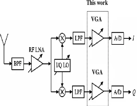
In particular direct conversion receiver (figure 1) which has attracted widespread attention for its simple architecture and easy integration with the base band circuit, as well as for its low power consumption and low manufacturing costs [4]. According to figure 1, the block diagram of a direct conversion receiver is presented receiver section of an integrated where spectrum receiver operating in the 863– 870 MHz. This receiver architecture directly down converts the signal to base band rather than converting it into an intermediate frequency (IF) first, and image rejection is no longer necessary in this approach. In the first, the RF signal that comes out of the antenna is filtered by the band pass filter
(BPF).Then, it is amplified by the low noising amplifier (LNA)before being down converted directly to base band along parallel in-phase (I) and quadrature (Q) signals. The frequency translation is performed by using two mixers using 0° and 90° phase shifted local oscillator (LO) signals. Finally, the I and Q base band signals are low pass filtered and amplified with variable gain amplifier (VGA) before the analogue to digital converter (A/D) conversion is intervened. In this case VGA is used to maximize the dynamic range of the system. It plays an important role of stabilizing the amplitude of a signal of interest under various conditions, providing constant amplitude signal in the signal path.
VGA
[image:1.595.317.542.426.599.2]VGA
This work
Figure 1: Block diagram of a direct conversion receiver or homodyne architecture
This paper addresses the design of a 220MHz VGA with 22 dB of gain range. The CMOS VGA architecture is based on a differential pair stage with voltage to current (V-I) converter, in which the gain is varied by changing the input voltage (Vin) from -1V to 0V. Then the output signal is
sampled by the discret-time low pass Sigma-Delta (εΔ) modulator and then processed by the digital block. The two-stage VGA was analyzed and designed in Austriamicrosystems (AMS) 0.35µm CMOS technology.
converter in which all simulations are specified, and full comparison of the performance of each VGA design are presented. Section 4 presents our conclusion.
2.
RECEIVER SPECIFICATION
The main objective of a receiver for wireless communication applications is to recover the base band signals that are modulated on a carrier wave at radio frequencies.
The design of a high performance, low power integrated radio frequency receiver in mainstream silicon technologies CMOS is a very challenging task involving numerous tradeoffs during the design process, especially between noise, linearity and power consumption.
To achieve the objective cited above, all aspects of the receiver and radio system (Base band, Modulation scheme, hopping bandwidth, data rate, Sensitivity, Maximum range, BER...) must be responded [5].
To characterise the sensor thermal noise (Nt) is given by:
dB
f
N
t
174
10
log
10(
b)
125
(1)
Another two elements defining sensor are SNRin, SNRout
(Signal to Noise Ratio) which are based on the following formula:
dB
N
S
SNR
in
t
23
(2)
dB
D
f
N
E
SNR
bdB b
out
10
log
105
0
(3)As shown in figure 2, ( Eb /N0 ) is equal to 11 with Noncoherent Frequency Shift Keying ̎ NC-BFSK ̎ to attenuate a bit error rate (BER) of 10-3 which is based on the following formula:
o N
b E
BFSK
NC
e
BER
21
2
1
(4)
with D represented data rate of 20 Kbps. [image:2.595.316.541.90.308.2]
11
Figure 2: Bit error rate (BER) for BPSK, C-BFSK and NC-BFSK
In order to realize a low power integrated radio frequency receiver used for wireless sensor receiver, we must respond to technological specifications and requirements listed in Table 1.
Table 1. Summarize table of wireless sensor receiver specification
Parameters Value
Base band frequency (fb) 80 KHz
Modulation scheme BFSK
Hopping bandwidth 7 MHz (863-870)MHz
Channels number 58
Data rate (D) 20 Kbps
Maximum range 50 m
BER 10-3 @ Eb/No=11dB Sensitivity (S) -102 dBm
3.
VGA DESIGN AND SIMULATIONS
3.1
VGA and Sigma-Delta analog to digital
converter (ADC)
Delta Sigma
Modulator
Digital Low
Pass Filter
Analog
signal in
Digital
signal out
VGA
This Work
Figure 3: Block diagram of the A/D converter with VGA
The Block diagram (Figure 3) is described as follows: the analog input signal enters the variable gain amplifier front-end stage, which translates this signal to the processing frequency, providing gain control to adjust its dynamic range, the selected signal is sampled by sigma-delta (εΔ) modulator and then processed by the digital low pass filter. Here, VGA plays an important role in supplying a constant-amplitude signal to the Sigma-Delta analogue to digital converter.
Sigma-Delta (εΔ) analog to digital converters (ADC) have been successful in realizing high resolution consumer. With VGA, (εΔ) converters are well suited for low bandwidth, high-resolution acquisition, and low cost, making them a good ADC choice for many applications such as wireless sensor. The effective number of bits of Sigma-Delta (Neff) converter
is given by [6]:
2 2L1 2L
2
eff
log
2N
1
2L
1
OSR
π
2
1
N
(5)
Where N represents number of bits of the quantization circuitry (N = 1), L represents order of modulator (L = 2) and OSR means Over Sampling Ratio which is based on the following formula:
b s
f
F
OSR
2
(6)
To simplify the decimator design, the oversampling ratio is usually chosen in powers of 2 and hence 128 has been chosen as the oversampling ratio, we obtain an effective number of 15.95 bits. Fs is the sampling frequency which is calculated to
10.240MHz, and fb means base band frequency (80 KHz).
[image:2.595.59.277.519.707.2]International Journal of Computer Applications (0975 – 8887) Volume 43– No.8, April 2012
3.2
VGA performance
Variable gain amplifiers (VGAs) are essential components of many communication and electronics systems. In a radio frequency (RF) transceiver, the received signal typically has a high dynamic range. In order to supply a signal of constant amplitude to a base band section of the transceiver, a variable gain amplifier (VGA) with equivalent or better dynamic range is required. VGAs can be found in many applications and are used to maximize the dynamic range of overall systems in medical equipments, telecommunication systems, wireless sensor receiver, hearing aids, disk drives, and others. In wireless sensor receiver the VGAs play the important role of stabilizing the amplitude of the output signal under various conditions and supply a constant-amplitude signal to the Sigma-Delta analogue to digital converter.
The most demanding characteristics of a variable gain amplifier (VGA) are Noise Figure (NF), the third-order Intermodulation Intercept point (IIP3), compression Point
(P-1) and Blocking Dynamic Range (BDR). The VGA
specifications are calculated and presented below: The Noise Figure (NF) is defined as:
dB dB SNR dB SNR SNR
SNR
NF in out
out in
18 ) ( )
(
(7)
Where SNRin and SNRout are input and output Signal to
Noise Ratio.
In order to determine the third-order intermodulation intercept point (IIP3), we firstly calculate the intermodulation product
(IMR) by this expression:
dBm
SNR
P
P
IMR
in
test
out
41
(
99
)
5
63
(8)Where we estimate ( Pin) the power levels of intermodulation
interference equal to -41 dB. Ptest is the test signal power
given by:
dBm
S
P
test
3
99
(9)Where S represents the sensitivity of -102 dBm. We obtain the third-order intermodulation intercept point (IIP3) by:
dBm
P
IMR
IIP
3
0
.
5
in
9
.
5
(10)Compression point (P -1 ) is given by :
dBm
IIP
P
1
3
10
19
.
5
(11)The Blocking Dynamic Range (BDR) can be expressed by:
dB
S
P
BDR
1
19
.
5
(
102
)
82
.
5
(12) [image:3.595.318.538.85.155.2]In order to achieve a novel structure of VGA with low power and high performance all aspects of the wireless sensor receiver must be respected. A summary of the VGA performance is listed in Table 2.
Table 2. Performance summary
Parameters Value
Noise figure (NF) 18 dB
Third-order intermodulation intercept point (IIP3)
-9.5 dBm
Compression point (P-1) -19.5 dBm
Blocking Dynamic Range (BDR) 82.5 dB
In a variable gain amplifier, a control unit will provide a gain signal to the variable gain amplifier, and, based upon the gain signal. The variable gain amplifier will accordingly amplify an input signal by an amount corresponding to the gain signal, to obtain an amplifier output signal. In order for a signal of a constant level to be supplied to a base band terminal of the received signal, the variable gain amplifier must also have a high dynamic range. The VGA is a circuit that manually controls its gain in response to the amplitude of the input signal, leading to a constant-amplitude output.
3.3
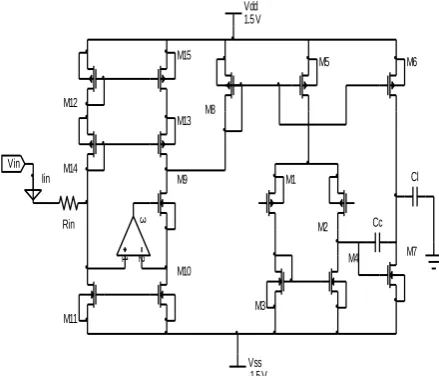
Circuit description
Figure 4 shows the architecture of the proposed VGA. It is composed of an Operational amplifier (op-amp)and a voltage to current (V-I) converter
A
A
B
B
C
C
D
D
E
E
F
F
G
G
H
H
I
I
J
J
1 1
2 2
3 3
4 4
5 5
6 6
7 Page: 1 of 1 Size: A No: 7
Rev: 46 16-Jan-2012 13:11 Created: 10-Nov-2011
File: C:\Users\radwene\Desktop\essai_TOP_SPICE\proposed_miller_OTA.sch M8
M5 M6
M1
M2
M4 M7
M3
Cc Cl Vdd
1.5 V
Vss -1.5 V Vin
M9
M10 1 2
3
M11 M12
M14
M15
M13
Rin Iin
Figure 4: Architecture of the proposed two-stage VGA
Firstly, operational amplifiers (op-amp) have sufficiently high voltage gain so that when the negative feedback is applied, the closed-loop transfer function can be made practically independent of the gain of the op-amp. This principle is employed in many useful analog circuits and systems such as our application. The primary requirement of an op-amp is to have an open loop gain which is sufficiently large to implement the negative feedback concept. The OTA is made up of three stages even though it is often referred to as a ―two-stage‖ op-amp, ignoring the buffer stage. The latter introduces an important concept of compensation. The primary goal of compensation is to maintain stability when negative feedback is applied around the operational amplifier.
[image:3.595.315.535.335.523.2]International Journal of Computer Applications (0975 – 8887) Volume 43– No.8, April 2012
use of PMOS input devices also provides reduced power supply rejection thanks to the current mirrors, and low sensitivity to change in power supply voltage. This first stage of op-amp also had the current mirror circuit formed by an N-channel MOSFETs, M3 and M4. The transistor M7 serves as an P-channel common source amplifier which is the second stage of op-amp. The current Ibias of the op-amp circuit goes
through current mirrors formed by P-channel MOSFETS, M8, M5 and M6. It is designed to produce a variable current between 10 μA and 150µA.
Secondly, as shown in figure 5 a proposed voltage to current converter is presented. This circuit offers a comparison between drain source voltage of M1 and M2 by using a differential amplifier to provide higher accuracy of the current copy. The input injection current signal Iin is formed by
variable input voltage Vin with resistance Rin. On the one
hand, we obtain a reduction of the input impedance which given by this relation:
olinp in
A
gm
R
.
1
1
(13)
and a very high output impedance, its value is:
amp op MC
olout
out
ro
A
ro
Av
Av
R
2.
2.
2.
(14)
Where gm and ro are the small-signal transconductance gain and the output resistance of the MOS transistors. In this case we assume that the amplifier have an input open-loop gain Aolinp and output open-loop gain Aolout (Aolout =AvMC2.Avomp).
AvMC2 and Avop amp denote the voltage gain of the transistor
MC2 and amplifier gain respectively.
A A B B C C D D E E F F G G H H I I J J 1 1 2 2 3 3 4 4 5 5 6 6
7 Page: 1 of 1 Size: A No: 7
Rev: 49 16- Jan- 2012 14: 07 Cr eat ed: 10- Nov- 2011
File: C: \ User s\ r adwene\ Deskt op\ essai_TO P_SPI CE\ new_m iller _O TA88. sch Vin M C2 M 2 1 2 3 M 1 Rin M P2 M P4 M P1 M P3 Vd d 1 . 5 V
Ro u t
[image:4.595.320.523.77.331.2]Vs s - 1 . 5 V I in
Figure 5 : proposed voltage to current converter
On the other hand, the drain source voltage of the mirror transistor M1 achieves a small constant value thanks to current source Iin and variable voltage source Vin. Drain
source voltage can be decreasing to a minimum value, by selection of Vin from -1V to 0V and consequently a very low
input voltage of the circuit.
A A B B C C D D E E F F G G H H I I J J 1 1 2 2 3 3 4 4 5 5 6 6
7 Page: 1 of 1 Size: A No: 7
Rev: 49 16-Jan-2012 04:18 Created: 10-Nov-2011
File: C:\Users\radwene\Desktop\essai_TOP_SPICE\essai00.sch MP1 MP2 MN2 MN1 Vdd Vss 1 2 3
A B C D E F G H I J
1 1 2 2 3 3 4 4 5 5 6 6
7 Page: 1 of 1 Size: A No: 7
Rev: 53 16-Jan-2012 12:10 Created: 10-Nov-2011
File: C:\Users\radwene\Desktop\essai_TOP_SPICE\essai00.sch MN2 Vdd 1 2 3 MN1
(a) (b)
2
3
1
Ibias
V
DDIbias
M5 M6
M7
Ibias/2
1
2
3
(b)
Figure 6: amplifier configuration:
(a) Simple differential amplifier structure [8] (b) Two-transistor amplifier structure [9]
In order to achieve high current copy accuracy, it is necessary to use an amplifier between the mirror’s input and output transistors.
The amplifier architectures are: simple differential amplifier and amplifier proposed by K. tanno. As shown in figure 6(a) [8], this structure is formed by the input differential pair (MP1 and MP2) and the active charge (MN1 and MN2). The figure 6(b) [9] shows a differential amplifier with two MOS transistors (MN1 and MN2) in which MN1 is operated in the weak version region (source gate voltage of MN1 equal to zero).This version can operate either in the linear region or in the saturation region for achieving low voltage and low consumption. For this reason we use this structure in our circuit.
-1.1 -1.0 -0.9 -0.8 -0.7 -0.6 -0.5 -0.4 -0.3 -0.2 -0.1 -0.0
Vin (V) 0 50 100 150
O
u
tp
u
r C
u
rre
n
t (
u
A
)
R
out= 100 Ω
R
out= 2.5 KΩ
R
out= 5 KΩ
[image:4.595.61.237.423.594.2]
For
Vin = - 1V Iout=10µAFigure 7: DC characteristics of V-I converter for different values of resistance Rout
Tspice simulations are carried for load resistor of 100 Ω. For an input voltage Vin varied from -1.1V to 0V, Figure 7 shows
[image:4.595.322.539.543.699.2]International Journal of Computer Applications (0975 – 8887) Volume 43– No.8, April 2012
of resistance (Rout=100 Ω, Rout=2.5 KΩ, Rout=5 KΩ) in which
the full input voltage swing capability is evident with truly linearity.
According to figure 8, the deviation of the DC output current from the ideal characteristic for different values of resistance Rout. The large error is reached for the lowest input voltage Vin
of -1.1V. On the other hand the variation of Vin between
-0.95V to 0V provide a small current error under 0.1% . For the maximum current error of 0.5%, Vin varied from -1.1V to
-0.95V.
[image:5.595.56.276.176.333.2]
R
out= 100 Ω
R
out= 2.5 KΩ
R
out= 5 KΩ
Figure 8: Current error of V-I converter
The figure 9 shows the AC characteristic of the proposed V-I converter. For a resistance of 100 Ω, we achieved a gain bandwidth (GBW) equal to 750 MHz, and 80.2 dB gain (Av).
100 1k 10k 100k 1M 10M 100M 1G 10G
Frequency (Hz)
60 65 70 75 80
C
u
rre
n
t
g
a
in
(d
B
[image:5.595.68.280.389.526.2])
Figure 9: Frequency response of proposed V-I converter
3.4
VGA Simulations
The schematic of the gain stages is provided in Figure 4. As shown in this figure, the current Ibias of the op-amp circuit
goes through current mirrors formed by P-channel MOSFETS, M8, M5 and M6. These transistors are used in strong inversion region to produce variable current.
The strong inversion region is the most frequently used among the three regions. In the strong inversion region, the commonly used drain current ID with VGS variation is
represented by the square law equation:
1
(
)
2
2
eff DS T
GS ox
D
V
V
V
V
L
W
C
µ
I
(15)In this expression, µ is the surface mobility of the channel, Cox
is the capacitance per unit area of the gate oxide, W is the effective channel width, L is the effective channel length, λ is the channel length modulation factor, VGS is the
gate-to-source voltage,VT is the nominal threshold voltage and VDS is
the resulting drain-to-source voltage.
The transconductance in the strong inversion region is [10]:
D ox
GS
m
I
L
W
C
µ
V
g
I
2
.
.
1 1
D
(16)
Where
I
D
I
5,
g
m
g
m1,
µ
µ
p(17)
In this work the gain bandwidth of OTA is given by this relation:
c m
C
g
GBW
.
.
2
1
(18)
From equation (16) we can simplify the gain bandwidth to:
5
I
K
GBW
(19)
Where K is constant expressed as:
c ox p
C
L
W
C
µ
K
.
.
2
.
2
1 1
(20)
As shown in figure 10 by using equation (19) and MATLAB simulation, the variation of output current of V-I converter from 10µA to 150µA provide a variations of the gain bandwidth from 80 MHz to 300 MHz
0 0.1 0.2 0.3 0.4 0.5 0.6 0.7 0.8 0.9 1 1.1 1.2 1.3 1.4 1.5 x 10⁻⁴ 0
80 160 240 320 350
Current (A)
G
BW
(MH
Z
)
Figure 10: GBW Vs output current of the voltage to current converter
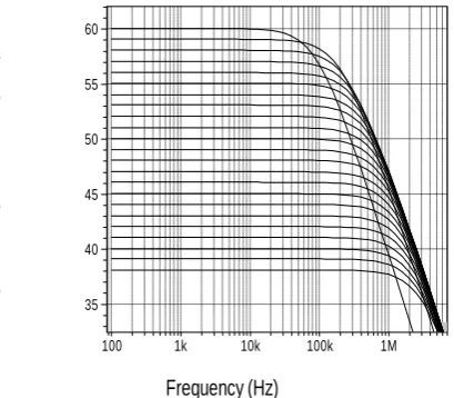
Figure 11 shows the simulated frequency response of the VGA over the entire gain range. As seen in the figure, the proposed design achieves the desired gain range of 22 dB in 1dB gain steps. The minimum bandwidth is 80 MHz, and the maximum bandwidth is limited to 300MHz for a load capacitance of 0.2 pf.
[image:5.595.318.539.461.615.2]Table 3. Performance comparison of this work and previously reported VGAs
100 1k 10k 100k 1M
Frequency (Hz)
35 40 45 50 55 60
V
o
lt
a
g
e
M
a
g
n
it
u
d
e
(d
B
)
Figure 11: Two-stage VGA gain response for 38 dB to 60 dB in 1 dB steps
4.
CONCLUSION
This work presents a novel design of a 220MHz VGA with 22 db of gain range. The architecture is based on a differential pair stage with voltage to current (V-I) converter, in which the gain is varied by changing the input voltage (Vin) from -1V to
0V. The variation of bandwidth is between 80 MHz and 300 MHz. Behavioural simulation indicated that the proposed design achieves the desired gain range of 22 dB in 1 dB gain steps and consume a minimum power of 0.5mW.
The design technique proposed in this paper combines better performance with simplicity of design and suitability of low energy. These parameters are very important in order to design Sigma-Delta ADC converter
5.
REFERENCES
[1] Chun-Hsien Wu and Yeh-Ching Chung :"Heterogeneous Wireless Sensor Network Deployment and Topology Control Based on Irregular Sensor Model," Advances in Grid and Pervasive Computing Lecture Notes in Computer Science, Volume 4459/2007,2007
[2] E.J, Duarte-Melo and Mingyan Liu : "Analysis of energy consumption and lifetime of heterogeneous wireless sensor networks," Global Telecommunications Conference , 2002. GLOBECOM ’02. IEEE, vol.1, no., 17-21 Nov 2002
[3] Trung kien Nguyen, Nam Jin Oh, and Viet Hoang Le, and Sang_Gug Lee, Member IEEE "A Low Power CMOS Direct Conversion Receiver With 3dB NF and 30KHz Flicker-Noise Corner for 915-MHz Band IEEE 802.15.4 ZigBee Standard," IEEE Transaction on Microwave Theory and Techniques 2006
[4] Ahmadreza Rofougaran, Glenn Chang, Jacob J. Rael, James Y.-C.Chang, Maryam Rofougaran, Paul J. Chang, Masoud Djafari, Jonathan Min, Edward W. Roth, Asad A. Abidi, and Henry Samueli, ―A Single- Chip 900-MHz Spread-Spectrum Wireless Transceiver in 1-μm CMOS—Part II: Receiver Design,‖ IEEE journal of solid-state circuits, vol. 33, no. 4, april 1998
[5] Trabelsi.H, Bouzid.Gh, Jaballi.Y, Bouzid.L, Derbel.F and Masmoudi.M : "A 863-870-MHz Spread-Spectrum Direct Conversion Receiver Design for Wireless sensor" IEEE DTIS'06, Tunisia, September, 2006
[6] Medeiro F., del Rio R., de la Rosa J.M., Pérez-Verdù B., A Sigma-Delta modulator design exemple : from specs to measurements, Baecelonea, May 6-10, 2002 .
[7] David Johns and Kenneth W. Martin : "Analog Integrated Circuit Design" John Wiley & Sons, 1997. [8] Ahmed Nader Mohieldin, Edgar Sánchez-Sinencio, and
José Silva- Martínez : ’ Nonlinear effects in pseudo differential OTAs with CMFB’, IEEE Transactions On Circuits and Systems-II: Analog and Digital Signal Processing, Vol. 50, No. 10, October 2003.
[9] K. tanno, O. Ishizuka and Z. Tang : ’ Low voltage and low frequency current mirror using a two- MOS subthreshold op-amp’, Electronics Letters 28th March 1996 Vol. 32 No. 7
Reference
CMOS process
Bandwidth (MHz)
Supply Voltage(V)
Power (mW)
Gain range(dB)/ no.of stages
Min. And Max gain (dB)
IIP3 (dBm) @ Gmin
P-1 (dBm)@
Gmin
NF (dB) @ Gmin
Gain control
[11] 0.25µm 30~210 2.5 27.5 80/4 -35~55 7 -8 8 Analogue
[12] 0.35µm 10 3 35 60/3 * * * * Analogue
[13] 0.18µm 32~1050 1.8 6.48 95/2 -52~43 * -17 * Analogue
[14] 0.25µm 380 2.5 63.25 80/4 -70~11 * * 11 Analogue
[15] 0.5µm 150 3.3 12.5 15/1 -5~10 * * * Analogue
[16] 0.35µm 21 1.5 24.8 26/1 -6~20 * * * Analogue
[17] 2 µm ~6 3 2.88 30/1 -0.4~29 * * * Analogue
[18] 0.35µm 125 3.3 21 19/1 0~19 35 * * Digital
[19] 1.2 µm 18 3 * 60/2 * * * * Digital
[20] 0.35µm 95 3.3 32.7 70/3 -30~40 -1.96 0.61 * Digital
[21] 0.8µm 15 5 25 14/1 -2~12 * * * Digital
[22] 0.35µm 246 3 27 60/3 -15~45 -4 * <15 Digital
[23] 0.18µm 20 1.8 13.28 60/3 0~60 * * * Digital
[24] 0.25µm 18 3.1 18.7 24/2 * * * * Digital
[25] 0.18µm 140~270 1.8 11.8 75/3 -15~60 14.38 -2.35 12.5 Digital
This work
[image:6.595.65.270.322.501.2]International Journal of Computer Applications (0975 – 8887) Volume 43– No.8, April 2012
[10] D. J. Comer and D. T. Comer, Fundamentals of electronic circuit design. NewYork: John Wiley & Sons Inc., 2003
[11] Y. Yamaji, N. Kanou, and T. Itakura, ―A temperature-stable CMOS variable-gain amplifier with 80 dB linearly controlled gain range,‖ IEEE J. Solid-State Circuits, vol. 37, no. 5, May 2002, pp. 553–558.
[12] Y. Zheng, J. Yan, and Y.P. Xu, ―A CMOS dB-linear VGA with pre-distortion compensation for wireless communication applications,‖ in Proc. IEEE Int. Symp. Circuits Syst., vol. 1, May 2004, pp. 813–816
[13] Q.-H. Duong, Q. Le, C.-W. Kim, and S.-G. Lee, ―A 95 dB linear low-power variable gain amplifier,‖ IEEE Trans. Circuits Syst. I, vol. 53, no. 8, Aug. 2006, pp. 1648–1657.
[14] O. Watanabe, S. Otaka, M. Ashida, and T. Itakura, ―A 380MHz CMOS linear-indB signal-summing variable gain amplifier with gain compensation technique for CDMA systems,‖ in Digest Tech. Papers Symp. VLSI Circuits, June 2002, pp. 136–139.
[15] P.-C. Huang, L.-Y. Chiou, and C.-K.Wang, ―A 3.3V CMOS wideband exponential control variable-gain-amplifier,‖ in Proc. IEEE Int. Symp. Circuits Syst., vol. 1, May1998, pp. 285–288.
[16] M. Green and S. Joshi, ―A 1.5V CMOS VGA based on pseudo-differential structures,‖ in Proc. IEEE Int. Symp. Circuits Syst., vol. 4, May 2000, pp. 461–464.
[17] A. Motamed, C. Hwang, and M. Ismail, ―A low-voltage low-power wide-range CMOS variable gain amplifier,‖
IEEE Trans. Circuits Syst. II, vol. 45, no. 7, July 1998, pp. 800–811.
[18] C.-C. Hsu and J.T. Wu, ―A highly linear 125MHz CMOS switched-resistor programmable-gain amplifier,‖ IEEE J. Solid-State Circuits, vol. 38, no. 10, Oct. 2003, pp. 1663–1670.
[19] H. Elwan and M. Ismail, ―Digitally programmable decibel-linear CMOS VGA for low-power mixed-signal applications,‖ IEEE Trans. Circuits Syst. II, vol. 47, no. 5, May 2000, pp. 388–398.
[20] C.-C.Wang, C.-L. Lee, L.-P. Lin, and Y.-L. Tseng, ―Wideband 70 dB CMOS digital variable gain amplifier design for DVB-T receiver’s AGC,‖ in Proc. IEEE Int. Symp. Circuits Syst., vol. 1, May 2005, pp. 356–359. [21] J.J.F. Rijns, ―CMOS low-distortion high-frequency
variable-gain amplifier,‖ IEEE J Solid-State Circuits, vol. 31, no. 7, July 1996, pp. 1029–1034.
[22] M.A.I. Mostafa, S.H.K. Embadi, and M.A.I. Elmala, ―A 60 dB, 246MHz CMOS variable gain amplifier for subsampling GSM receivers,‖ in Proc. Int. Symp. Low Power Electronics and Design, Aug. 2001, pp. 117–122. [23] H. Dinc, P.E. Allen, and S. Chakraborty, ―A low
distortion, current feedback, programmable gain amplifier,‖ in IEEE Int. Symp. Circuits Syst., vol. 5, May 2005, pp. 4819–4822.