Bit Swapping and Cell Ordering on Finding Faults
in Test Pattern Generation using BIST
Anandhi.K1, Shouba Tharani. J2
1, 2Pg Scholar, Kpr Institute of Engineering and Technology, Coimbatore, India.
Abstract: Testing for delay and stuck-at faults requires two pattern tests and test sets are usually large. Built-in self-test (BIST) schemes are attractive for such comprehensive testing. The BIST test pattern generators (TPGs) for such testing should be designed to ensure high pattern-pair coverage. In the proposed work, necessary and sufficient conditions to ensure complete/ maximal pattern-pair coverage for sequential circuit has been derived. A new low power weighted pseudorandom test pattern generator using weighted test-enable signals is proposed using a new clock disabling scheme .It supports both pseudorandom testing and deterministic BIST. To implement the low power BIST scheme, a design-for-testability (DFT) architecture is presented. During the pseudorandom testing phase, an LP weighted random test pattern generation scheme is used by disabling a part of scan chains.A novel low-power bit-swapping LFSR (BS-LFSR) is used to minimize the transistions, while keeping the randomness almost similar. The BS-LFSR is combined with a scan-chain-ordering algorithm that orders the cells in a way that reduces the average and peak power (scan and capture) in the test cycles (or) while scanning out a response to a signature analyzer. These techniques have a substantial effect on average and peak power compared to the existing approach.
Keywords: Bit swapping, Scan chain reordering, Delay fault and Stuck-at-Fault, Design for testability and test pattern generation.
I. INTRODUCTION
two-pattern tests are applied to the combinational CUT. The capability of a TPG to generate two-two-pattern tests is measured by the metric transition coverage. The main focus of this paper is to identify necessary and sufficient conditions for commonly used TPGs (namely, LFSRs and CA) to achieve complete/maximal transition coverage. The number of possible ways to achieve the optimal transition coverage for each TPG type is derived. Efficiency of TPGs designed with these conditions are validated by robust path delay fault simulation on synthesized benchmark circuits.
II. RELATED WORK
In common, most of the pattern compression methods discussed in the literature employ one or other form of circuit modification or circuit addition. This leads to increase in area, test power and test time. Also these techniques are proposed for the development of new designs and are not suitable for already existing designs. No solutions suggested to reduce random test patterns size to an already logic BIST inserted fabricated chip. The work proposed in this thesis introduces a novel test patterns compression algorithm called seed selection algorithm based on a position of test vector in exhaustive test pattern set generated by Logic BIST. Position of vector can easily be computed by LFSR Characteristic polynomial. The compression algorithm exploits pre-computational property of Characteristic polynomial. Also a low-overhead scheme for achieving complete fault coverage during built-in self -test of circuits with scan is presented. It does not require modifying the function logic and does not degrade system performance. Deterministic test patterns that detect the random-pattern-resistant (r.p.r.) faults are embedded in a pseudorandom sequence of bits generated by a linear feedback shift register (LFSR) [11]. Also literature survey shows that no proper solutions exist to protect the internal logic BIST circuitry from hacking. In this thesis a security method is proposed for the device that uses structured DFT techniques like LBIST and boundary scan. This security scheme will prevent unauthorized users from hacking the JTAG interface and accessing the logic BIST test functions. Security is provided in two stages. First stage security is provided to the JTAG port using multi-level locking mechanism. Second stage protection is given to the logic BIST by incorporating a configuration register. Multiple
cryptographic algorithm based encrypted private key storage module is implemented in logic BIST. Here separate authentication module is provided for the JTAG and logic BIST. It adds only small area overhead to the device. This proposed approach will secure the devices to great extent during testing. The main contributions of the research presented in this work are as follows: 1.Scalable pattern mapping and Seed Selection for shortest test sequence approach: An innovative approach has been introduced for mapping deterministic patterns to a pseudo-random test sequence. This approach relies on the condensed LFSR concept and proposes the definitive nature of the deterministic patterns being a subset in the exhaustive test set. This method does not add any
circuitry and can be employed on already LBIST inserted designs also. It selects the prospective seeds (starting value of the LFSR) and puts them in a ROM memory in the LBIST structure. The fault coverage of stuck at fault (modelled defects) by pseudo-random sequences is evaluated and analyzed. The impact of the length of the seed selection based test sequences on the test coverage of the modeled defects and test cycles per net have been investigated as well. 2. Multilevel security for logic BIST circuits: An innovative multilevel security approach for on-chip test structures is employed. In order to improve cracking difficulty, the programmable key
length scheme has been implemented with a combinational logic module for comparison of different levels of access. Possible key
length, hardware overhead and cracking difficulty level have been analyzed. 3. Innovative Crypto keys based security register approach: An important achievement of this work is a crypto keys based security register, which is used to enable and improve the security based on multiple crypto algorithms and reconfigurable register structure.
III. PROPOSED SEYSTEM OF LFSR
A linear feedback shift register (LFSR) is a shift register whose input bit is a linear function of its previous state. The only linear functions of single bits are xor and inverse-xor; thus it is a shift register whose input bit is driven by the exclusive-or (xor) of some bits of the overall shift register value. The initial value of the LFSR is called the seed, and because the operation of the register is deterministic, the sequence of values produced by the register is completely determined by its current (or previous) state. Likewise, because the register has a finite number of possible states, it must eventually enter a repeating cycle [12]. However, an LFSR with a well-chosen feedback function can produce a sequence of bits which appears random and which has a very long cycle.
LFSR output streams are deterministic. If you know the present state, you can predict the next state. This is not possible with truly random events such as nuclear decay. The output stream is reversible; an LFSR with mirrored tap sequence will cycle through the states in reverse order.
A. Bit swapping LFSR
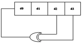
The bit-swapping LFSR (BS-LFSR), is composed of an LFSR and a 2 × 1multiplexer shown in fig 1. When used to generate test
patterns for scan-based built-in self-tests, it reduces the number of transitions. The proposed BS-LFSR generates the same number of 1s and 0s at the output of multiplexers after swapping of two adjacent cells; hence, the probabilities of having a 0 or 1 at a certain cell of the scan chain before applying the test vectors are equal. Hence, the proposed design retains an important feature of any random TPG. In the BS-LFSR, consider the case that c1 will be swapped with c2 and c3 with c4..., cn−2 with cn−1 according to the value of cn which is connected to the selection line of the multiplexers. In this case, we have the same exhaustive set of test vectors as would be generated by the conventional LFSR, but their order will be different and the overall transitions in the primary inputs of the CUT will be reduced.
Fig 1. 2*1 multiplexer LFSR
[image:3.612.240.401.268.357.2]The proposed BS-LFSR for test-per-scan BISTs is based upon some new observations concerning the number of transitions produced at the output of an LFSR. Two cells in an n-bit LFSR are considered to be adjacent if the output of one cell feeds the input of the second directly (i.e., without an intervening XOR gate).
Fig 2 Bit Swapping LFSR for c1 to cn arrangement
Each cell in a maximal-length n-stage LFSR (internal or external) will produce a number of transitions equal to 2n−1 after going through a sequence of 2n clock cycles shown in figure 2. The sequence of 1s and 0s that is followed by one bit position of a maximal-length LFSR is commonly referred to as an m sequence. Each bit within the LFSR will follow the same m-sequence with a one-time-step delay. The m-sequence generated by an LFSR of length n has a periodicity of 2n − 1. It is a well-known standard property of an m-sequence of length n that the total number of runs of consecutive occurrences of the same binary digit is 2n−1 [12]. The beginning of each run is marked by a transition between 0 and 1.
B. Scan-Chain Ordering
[image:3.612.224.429.439.536.2]The steps in this algorithm are as follows.
1) Simulate the CUT for the test patterns generated by the BS-LFSR
2) Identify the group of vectors and responses that violate the peak power
3) In these vectors, identify the cells that mostly change their values in the test cycle and cause the peak-power violation 4) For each cell found in step 3), identify the cells that play the key role in the value of this cell in the test cycle
5) If it is found that, when two cells have a similar value in the applied test vector, the concerned cell will most probably have no transition in the test cycle, then connect these cells together.
If it is found that, when two cells have a different value, the cell under consideration will most probably have no transitions in the test cycle, then connect these cells together through an inverter.
Fig 3 Block diagram of bit swapping and scan chain reordering algorithm for BIST technique
C. Weighted Pseudorandom Hybrid BIST
This section describes the basic idea of the proposed scheme for hybrid BIST with weighted pseudorandom testing. Implementation details are explained in subsequent sections. Fig.3 shows a block diagram of the test architecture. In this scheme, 3-valued weights are used for three possible weights for a specific scan element are 0, 1, and (which signifies “unbiased”). A weight of 0 forces the value of a particular scan element to 0, a weight of 1 forces it to 1, and a means that the scan element takes on a value of 0 or 1 with equal probability. In Fig. , the scan elements of the chip have been configured into scan chains each of which contains scan elements (bits). Since a 3-valued weight system is being used, two bits are required to store the weight for each scan element.
Fig 4. Illustrates the STUMPS architecture for BIST where at each clock cycle, (one bit into each scan chain).
the system clock is applied and the output response is captured in the scan chains. This output response is shifted out and compacted in the multiple input signature register (MISR) [13] as the next test vector is shifted in.
The weight bits for the scan chains are stored in one location of the LUT. At each clock cycle, the tester supplies an LUT index which is used to read the weights for the bits from the LUT. These weights are then used to transform the pseudorandom bits coming from the PRPG as they are shifted into the scan chains. The tester and the PRPG operate at the same clock frequency in a lock-step manner. The number of bits required for the LUT index depends on the size of the LUT. The number of bits, required for the index is generally much less than So in this scheme, tester channels are being used to drive scan chains, where is much less than. Hence, the test bandwidth requirements are being reduced. For each weight set, a sequence of LUT indices are stored on the tester. If weighted pseudorandom patterns are to be generated for each weight set, then the tester simply resends the sequence of indices for each weight set times. Only one copy of the sequence of indices for each weight set needs to be stored in the tester memory. There are three levels of compression in this scheme. The first level of compression is that only the unique parts of each weight set need to be stored in the LUT thus for each weight set there will much less than rows in the LUT. The second level of compression is that each weight set is stored as a sequence of -bit indices on the tester where scales logarithmically with the number of rows in the LUT and is much less than the third level of compression is that each weight set is expanded into weighted pseudorandom test patterns. These three levels of compression result in greatly reduced tester storage requirements and tester bandwidth requirements.
D. Circuit Under Test
The BS-LFSR is evaluated regarding the length of the test sequence needed to achieve certain fault coverage is shown in fig 3. The scan-chain-ordering is performed in the circuit under test in order to reduce the capture power. The experiments were performed on full-scan ISCAS’89 benchmark circuits and the percentage of redundant faults in the CUT, and fault coverage is analyzed.
E. Response Analyzer
The response analyzer is used to compare the expected result with the response obtained from the circuit under test. And with this response the fault coverage of the circuit under test is analyzed.
F. Cell Reordering Algorithm:
1) Simulate the CUT for the test patterns generated by the BS-LFSR
2) Identify the group of vectors and responses that violate the peak power
3) In these vectors, identify the cells that mostly change their values in the test cycle and cause the peak-power violation 4) For each cell found in step 3), identify the cells that play the key role in the value of this cell in the test cycle
5) If it is found that, when two cells have a similar value in the applied test vector, the concerned cell will most probably have no transition in the test cycle, then connect these cells together. If it is found that, when two cells have a different value, the cell under consideration will most probably have no transitions in the test cycle, then connect these cells together through an inverter. Although the proposed BS-LFSR can achieve good results in reducing the consumption of average power during test and also in minimizing the peak power that may result while scanning a new test vector, it cannot reduce the overall peak power because there are some components that occur while scanning out the captured response or while applying a test vector and capturing a response in the test cycle. To solve these problems, first, the proposed BS-LFSR has been combined with a cell-ordering algorithm presented in that reduces the number of transitions in the scan chain while scanning out the BS-LFSR can be used to generate exhaustive patterns for test-per lock. This will reduce the overall average power and also the peak power that may arise while scanning out a captured response.
The problem of the capture power (peak power in the test cycle) will be solved by using a novel algorithm that will reorder some cells in the scan chain in such a way that minimizes the Hamming distance between the applied test vector and the captured response in the test cycle, hence reducing the test cycle peak power (capture power). In this scan-chain-ordering algorithm, some cells of the ordered scan chain using the algorithm will be reordered again in order to reduce the peak power which may result during the test cycle. This phase mainly depends on an important property of the BS-LFSR [11].
similar in 75% of the applied vectors. Hence, assume that we have cell x which is a function of cells y and z. If the value that cell x will have in the captured response is the same as its value in the applied test vector (i.e., no transition will happen for this cell in the test cycle) in the majority of cases where cells y and z have the same value, then we connect cells y and z together on the scan chain, since they will have the same value in 75% of the cases. This reduces the possibility that cell x will undergo a transition in the test cycle.
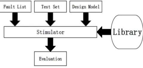
F. Fault Simulation
[image:6.612.184.423.233.347.2]The purpose of fault simulation is to guide the test pattern generation process, measure effectiveness of test patterns and generate fault dictionaries. Fault simulation needs three components: fault list, test set and design model. Given these components, fault simulation will determine fault coverage and set of undetected faults. In the VLSI testing world, there are a lot of fault simulation algorithms, such as serial, parallel, deductive and concurrent fault simulation. Figure shows the flowchart of fault simulation.
Fig 5 Fault Simulation Flow chart
IV. CONCLUSION
This paper surveys about the entire test pattern generation finding by using the bit swapping and scan chain reordering algorithm. And finding the faults in entire circuit, the identified faults are by observation point insertion in circuit to be tested. Stuck-At-Fault and Delay Faults are identified by point insertion. This survey is for future establishment of upcoming project. The Benchmark circuit of ISCAS’89 is used for testing under scan based BIST.
REFERENCES
[1] M.L. Bushnell and V.D. Agrawal, “Essentials of Electronic Testing”, Kluwer Academic Publishers, ISNB 0-7923-7991-8 2000 [2] A. Hertwig and H.J. Wunderlich, “Low Power Serial Built-In Self-Test”, IEEE European Test Workshop, pp. 49-53, 1998.
[3] S. Wang and S.K. Gupta, “ATPG for Heat Dissipation Minimization for Scan Testing”, ACM/IEEE Design Auto. Conf., pp. 614-619, 1997
[4] F. Corno, P. Prinetto, M. Rebaudengo and M. Soma Reorda, “A Test Pattern Generation Methodology for Low Power Consumption ’0 IEEE VLSI Test Symp., pp 453- 459, 1998.
[5] L. Whetsel, “Adapting Scan Architectures for Low Power Operation”, IEEE Int. Test Conf., pp. 863-872, 2000
[6] J. Saxena, K.M. Butler and L. Whetsel, “A Scheme to Reduce Power Consumption During Scan Testing”, LEEE Int. Test Conf., pp. 670-677, 2001
[7] V. Dahholkar, S. Chakravarty, I. Pomeranz and S.M. Reddy, ‘Techniques for Reducing Power Dissipation During Test Application in Full Scan Circuits”, IEEE Transactions on CAD, Vol. 17, No 12, pp. 1325-1333,December 1998
[8] P. Girard, C. Landrault, S. Pravossoudovitch and D. Severac, “Reducing Power Consumption during Test Application by Test Vector Ordering”, IEEE Int. Symp. On Circuits and Systems, CD-ROM proceedings, 1998
[9] P. Girard, L. Guiller, C. Landrault and S. Pravossoudovitch, “A Test Vector Ordering Technique for Switching Activity Reduction during Test Operation”, IEEE Great Lakes Symp. On VLSI, pp. 24-27, 1999
[10] Dong Xiang, Xiao Qing Wen, and Laung-Terng Wang, “Low-Power Scan-Based Built-In Self-Test Based on Weighted Pseudorandom Test Pattern Generation and Reseeding” IEEE transaction on very large scale integration (VLSI) systems, 1063-8210 © 2016
[11] A. S. Abu-Issa and S. F. Quigley, “Bit-swapping LFSR and scan-chain ordering: A novel technique for peak- and average-power reduction in scan-based BIST,” IEEE Trans. Computer.-Aided Design. Integration. Circuits Syst., vol. 28, no. 5, pp. 755–759, May 2009
[12] S. Banerjee, D. R. Chowdhury, and B. B. Bhattacharya, “An efficient scan tree design for compact test pattern set,” IEEE Trans. Computer. Aided Design. Integration. Circuits Systems. Volume. 26, no. 7, pp. 1331–1339, Jul. 2007