by modification of the molecule–substrate bond
Cai Shen1,2 and Manfred Buck*1
Full Research Paper
Open AccessAddress:
1EaStCHEM School of Chemistry, University of St Andrews, St Andrews KY16 9ST, United Kingdom and 2Ningbo Institute of Materials Technology & Engineering, Chinese Academy of Sciences, Ningbo, 315201, China
Email:
Manfred Buck* - [email protected]
* Corresponding author
Keywords:
copper; electrodeposition; gold adatoms; nanolithography; negative resist
Beilstein J. Nanotechnol. 2014, 5, 258–267. doi:10.3762/bjnano.5.28
Received: 21 November 2013 Accepted: 06 February 2014 Published: 10 March 2014
This article is part of the Thematic Series "Advanced atomic force microscopy techniques II".
Guest Editors: T. Glatzel and T. Schimmel
© 2014 Shen and Buck; licensee Beilstein-Institut. License and terms: see end of document.
Abstract
The intercalation of Cu at the interface of a self-assembled monolayer (SAM) and a Au(111)/mica substrate by underpotential depo-sition (UPD) is studied as a means of high resolution patterning. A SAM of 2-(4'-methylbiphenyl-4-yl)ethanethiol (BP2) prepared in a structural phase that renders the Au substrate completely passive against Cu-UPD, is patterned by modification with the tip of a scanning tunneling microscope. The tip-induced defects act as nucleation sites for Cu-UPD. The lateral diffusion of the metal at the SAM–substrate interface and, thus, the pattern dimensions are controlled by the deposition time. Patterning down to the sub-20 nm range is demonstrated. The difference in strength between the S–Au and S–Cu bond is harnessed to develop the latent Cu-UPD image into a patterned binary SAM. Demonstrated by the exchange of BP2 by adamantanethiol (AdSH) this is accomplished by a sequence of reductive desorption of BP2 in Cu free areas followed by adsorption of AdSH. The appearance of Au adatom islands upon the thiol exchange suggests that the interfacial structures of BP2 and AdSH SAMs are different.
Introduction
The applications of organic adsorbates for the electrodeposition of metals range from tuning the chemistry [1,2] to templating [3,4]. Contrasting the former where random assemblies are used, the latter relies on highly organised layers that comprise supramolecular networks [5,6] or self-assembled monolayers (SAMs) [3,4,7-18]. Exploiting variations in the interfacial charge transfer, SAMs are convenient systems to control the
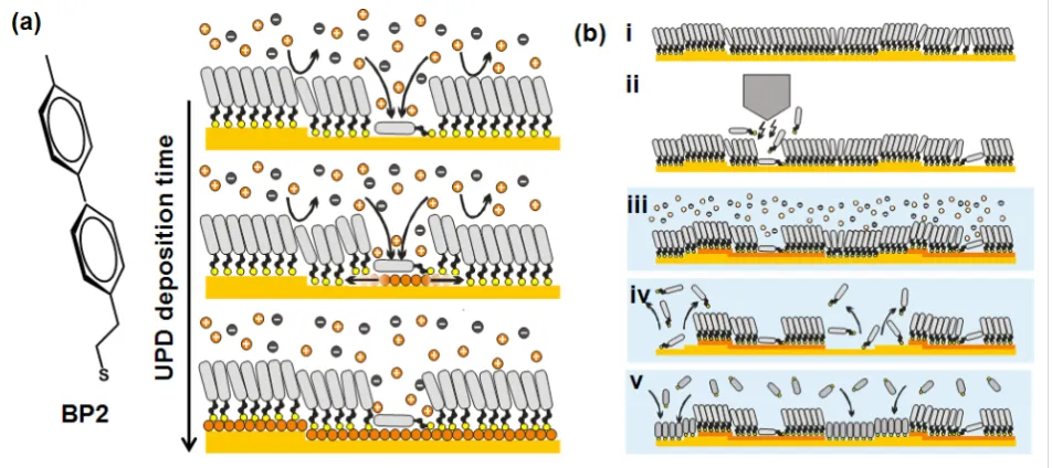
Figure 1: (a) Mechanism of Cu-UPD onto a BP2-modified Au(111) surface with the deposition starting at defects and the UPD proceeding by lateral diffusion of the metal atoms at the SAM–substrate interface. (b) Scheme illustrating the steps in UPD-based patterning. For details see text.
In contrast, UPD on SAM-modified electrodes yields a mono-or bilayer of metal, which is intercalated at the SAM–substrate interface [20-24]. The interest in this process arises from the al-teration in the strength of the S–substrate bond. Following the order Au < Ag < Cu [25] patterning is enabled by a localised UPD of Cu or Ag on Au and the subsequent reductive desorp-tion of the less tightly bound thiol molecules in the UPD-free Au areas to yield either nanoporous SAMs or binary SAMs in the case of backfilling with a second type of thiol [11]. So far, however, this approach has been lacking control as UPD is mediated by random defects [24,26,27] which, using standard SAMs such as alkanethiols, results in the arrangement of pores or domains of different thiols in a statistical fashion, thus, prohibiting patterning and controlling dimensions.
In order to overcome this bottleneck, SAMs are required that exhibit a structural perfection to an extent that UPD does not occur in the case of the native layer but only at defects intro-duced a posteriori by using lithographic techniques. In previous studies of our group it was found that SAMs of ω -(4'-methyl-biphenyl-4-yl)alkanethiols (CH3-C6H4-C6H4-(CH2)nSH, BPn) can form layers of exceptional structural perfection [24,28-30], as a consequence of the specific molecular architecture charac-terised by an aromatic moiety linked to the thiol head group by a short aliphatic chain (see Figure 1a). Designing the molecules such that different factors that determine the enthalpy of the system compete to some extent [28], these SAMs can undergo phase transitions to structures that exhibit the required blocking of UPD. On Au substrates this is the case if the aliphatic spacer chain consists of an even number of methylene units. Two prop-erties of the BPn SAMs are decisive for a patterned UPD
process. The first one is that imperfections intrinsic to these layers, i.e., defects that cannot be eliminated such as domain boundaries and atomic steps in the underlying substrate, do not impede the passivation of these SAMs against UPD. More substantial defects such as impurities already present on the substrate prior to SAM formation or explicit damaging of the SAM are required. The second one refers to the mechanism of UPD, which is illustrated in Figure 1a. Different from what has been reported for alkanethiols [22,27] the UPD process starts at defects and proceeds via lateral diffusion of the metal atoms at the SAM–substrate interface. Most importantly, the UPD metal is exclusively supplied through the defects, not only in the initial stages of the process but until the whole surface is covered [24]. A crucial feature of the process is that the interca-lation of the metal does not affect the passivating properties of the SAM. It is this defect- and diffusion-controlled UPD mecha-nism that forms the basis for the work presented here as patterned deposition becomes possible by a localised break down of the passivation and control over dimensions of UPD patterns will be exerted through the deposition time and/or the size of defects introduced.
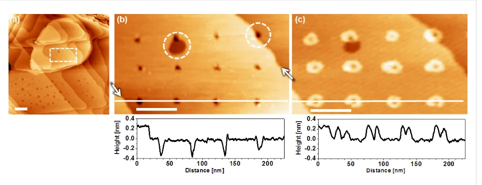
[image:2.595.61.537.524.736.2]Figure 2: Cu-UPD on Au templated by a patterned BP2 SAM. a) Large scale STM image of the surface before deposition recorded in air. (b) Magni-fied image of area marked in (a) revealing an array of point defects created by voltage pulses of 4.5 V applied to the STM tip for 50 ms. Steps in the Au substrate are highlighted by the arrows. Dashed circles mark defects at the edge of a vacancy island and step, respectively. (c) In situ electro-chemical STM image of the same area after Cu-UPD of 30 min at 0.275 V vs Cu2+/Cu. Height scales in the line profiles are normalised to the Au step height of 2.5 Å. All scale bars 50 nm.
however, noted that this restriction does not apply if one is not interested in mechanistic in situ studies.
The overall process is outlined in Figure 1b. Starting from a high quality SAM (i) defects are introduced (ii) under ambient conditions by applying voltage pulses to the tip [7,8,37,38]. Subsequently, the sample is exposed to the electrolyte that contains the metal ions and UPD is performed (iii). Since, as illustrated in Figure 1a, UPD proceeds via diffusion of the Cu atoms and the deposition rate increases with higher cathodic potentials, the lateral dimensions are determined by controlling deposition time and potential. The UPD-modified SAM can then be further processed by removing the first thiol and then backfill the empty areas by a second thiol (iv), thus, creating a patterned binary SAM (v). It is noted that steps iv/v can be conveniently performed in one setup by reductively desorbing the first thiol in the cathodic sweep of a voltammetric cycle and adsorb the other thiol during the anodic sweep.
Results and Discussion
Patterned UPD
STM images of the UPD of copper on a BP2-modified Au sub-strate are shown in Figure 2. The typical topography of the SAM-covered substrate is seen in Figure 2a. Due to the thermal treatment of the BP2 layer the smaller terraces are free of vacancy islands (VIs) and those present on more extended terraces are significantly bigger and less dense compared to samples prepared at room temperature. While Ostwald ripening accounts to some extent for this, the phase transition involved in the annealing is another process likely to contribute as discussed further below.
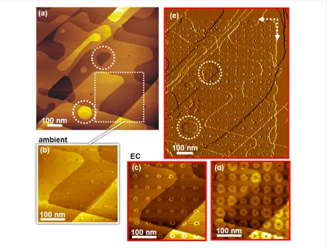
Figure 3: Temporal evolution of Cu-UPD. (a) Large scale ambient STM image of a native BP2 SAM on Au. (b) Magnified image of the area marked by the square in (a) after patterning with voltage pulses of 3.8 V for 50 ms. (c,d) EC-STM images of the area shown in (b) after different periods of UPD, 176 min (c) and 329 min (d) with the sample potential decreased from initially 0.4 V to 0.2 V vs Cu2+/Cu. (e) Large scale STM image after the UPD islands have coalesced to a uniform area. Circles in (a,e) mark identical areas. The dashed arrows in (e) mark boundary between UPD areas and passivated areas. (a–d) show constant current images, in (e) the derivative is shown for better visual differentiation between native and UPD modified areas.
is not affected to the extent that the passivation against UPD breaks down. There is no UPD outside the damaged areas, which confirms the excellent quality of the BP2 SAM.
In experiments, in which we varied the spot size of the damage we noticed that this significantly affects the rate of the UPD process. In agreement with the mechanism established for this type of SAMs [24] this is expected since the growth rate scales with the flux of Cu ions integrated across the defect area. Inter-estingly, a minimum size of the defect was observed to be required. For defects smaller than 5 nm, it is difficult to trigger the UPD, or even if the UPD starts, the UPD can easily be blocked during the UPD process. This further corroborates that, after removal of thiols by pulsing, thiols diffuse back into the defect from the surrounding area. Obviously, the SAM can bear a certain level of disorder/defects before the passivation against UPD breaks down. Even though it was not a focus of the
present study we note that the partial passivation of the defect by SAM molecules also requires substantially more cathodic potentials to initiate the deposition of bulk metal into these holes as compared to a clean Au substrate.
varia-Figure 4: Templated Cu-UPD illustrating tolerance of the process against substrate dislocations. (a) Native substrate with uniform BP2 SAM. (b) Lithographic pattern formed in air by using a tip bias of 4.2 V and a tip speed of 0.75 μm/s. (c) EC-STM images of Cu-UPD after 11 min at 0.16 V vs Cu2+/Cu. (d) Uniform UPD area after 32 min. Dotted lines and arrows in height profiles along lines shown in (b,c) mark substrate steps present in the native substrate and generated during UPD, respectively.
tions at the edges. As the deposition continues the UPD islands grow as evidenced by Figure 3d, which shows the pattern formed after 329 min. The islands are about 30–50 nm in size. Their circular shape is still maintained, which demonstrates that these Cu patterns were formed by the Cu2+ ions diffusing radi-ally out from the defects initiradi-ally created by the STM tip. Ulti-mately the island coalesce to form a uniform UPD area (Figure 3e), which in the example displayed was accomplished after 486 min at 200 mV. In order to make the uniform deposi-tion more easily visible, the derivative of the current is displayed in Figure 3e. The boundaries between the UPD and unmodified areas are marked by the dashed arrows and the features marked by the dashed circles provide the reference to the large scale image acquired in air prior to UPD.
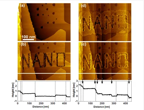
The procedure is not limited to point like defects as illustrated by Figure 4. By using a bias of 4.2 V and a tip speed of 0.75 μm/s continuous lines such as the letters are written. As for
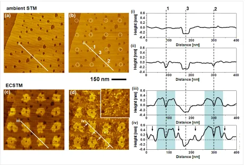
[image:5.595.62.537.352.715.2]preferen-Figure 5: Sequence of STM images showing the UPD-based conversion of a BP2 SAM into a patterned binary SAM of BP2 and AdSH. Left: (a) Native BP2 SAM. b) Array of defects (encircled) created by STM lithography while using voltage pulses of 3.5 V and 50 ms duration. (c) Pattern of Cu-UPD generated by holding the sample potential at +0.3 V vs Cu2+/Cu for 10 seconds. (d) Binary SAM structure after reductive desorption of BP2 and adsorption of AdSH. The inset shows an area of the sample, which had not been modified by Cu-UPD. Right: Compilation of height profiles along lines shown in the STM images illustrating the evolution of topography. Protrusions marked by arrows in (iv) reflect AdSH covered Au islands. For details see text.
tial diffusion of UPD metal along those steps. Thus, possible structural differences between a BP2 SAM that covers a native step in the initial preparation procedure and one being gener-ated during the UPD process are too small to alter the UPD mechanism. This is essential for the exploitation of this process on the nanoscale as the UPD pattern and, thus, its spatial resolu-tion is not impeded by processes that cannot be eliminated.
The ruggedness of the BP2 SAM structure against the genera-tion of Au steps, which is induced by the UPD, is in line with the preserved passivation of the monolayer at steps of Cu-UPD islands intercalated at the SAM–substrate interface [24]. However, the distinct generation of Au steps in the example presented above suggests that the STM patterning itself has an influence. While for a small point-shaped damage dislocations in the substrate occur rarely (none in Figure 2, one in Figure 3 intersecting the encircled island in the lower half of image (e)) the more extensive damage of the SAM by writing continuous lines (here in the form of letters) gives rise to a substantial number of substrate dislocations. This can be rationalized by
considering that at least the topmost Au layer is affected, which includes the removal of Au atoms together with thiol molecules.
Conversion of UPD pattern into binary SAM
structure
The SAM modified by the UPD pattern corresponds to a latent image, which has to be developed by, for example, conversion into a pattern that exhibits heterogeneous surface properties as illustrated in Figure 1b. As mentioned above this is conve-niently done by exploiting the differences in the strength of the S–metal bond between Au and Ag and Cu [25]. While the selec-tive removal of thiols from UPD-free Au areas has been exploited for the generation of nanoporous SAMs [11], the process lacked control as UPD occurred at defects present in the native monolayer. The approach based on the SAMs used here, which perfectly block UPD, allows for the exploitation of this principle for the controlled patterning on the nanoscale.
[image:6.595.59.539.377.702.2]and UPD modified BP2 SAM (c), as well as the binary SAM (d), where BP2 adsorbed on Au has been replaced by adaman-tanethiol (AdSH). The exchange was accomplished by performing a voltammetric cycle, in which the reductive desorption of BP2 and the adsorption of AdSH occured during the cathodic and anodic sweeps, respectively. In the present experiment a basic solution of AdSH in EtOH was used. The successful exchange of the thiol is probed by a second cyclic voltammogram. An anodic shift of the desorption potential by about 35–40 mV (see Figure S1 in Supporting Information File 1) is characteristic for the difference in stability between the two thiols [43]. The exchange is also evidenced by charac-teristic differences seen in the STM images recorded before (Figure 5c) and after (Figure 5d) the replacement of BP2 in the areas, which were not covered by UPD islands. The most obvious one is that the contours of the islands become rather ill-defined and protrusions appear in between the UPD islands. While, at first glance, this seems like a serious deterioration of the shape of the islands, a closer look reveals that the contours of the islands such as shape asymmetries and irregularities are rather well preserved. The topographical changes are mainly due to the restructuring of the Au surface upon desorption of BP2. The fact that exactly the same topographical changes occur in areas of the sample where the SAM has not been patterned (inset in Figure 5d) proves that these features are not related to Cu-UPD. The formation of the protrusions agrees well with other studies of thiol desorption [44,45] and is explained by the formation of Au islands from Au adatoms present at the SAM–Au interface [46-48]. There is, however, a difference between the present study and other studies, in which island formation has been observed. Any Au islands formed during the desorption of BP2 should be consumed again when the other thiol is adsorbed. The extent to which this occurs is dependent on how similar the structures of the SAM–substrate interface are for the two thiols. Since the adamantanethiol packs less dense compared to BP2 (≈40 Å2 per molecule compared to ≈29 Å2) it is expected that Au islands remain after the adsorption of the adamantanethiol. However, the integrated area covered by the islands is unexpectedly large. Assuming that the number of Au adatoms involved is identical for BP2 and AdSH and that the same bonding configuration discussed for alkanethiols is adopted involving either one Au adatom per molecule or shared between two thiols, the area covered by islands should be about 3.5–7.0% of a monolayer after the exchange. This is significantly smaller than the experimentally observed area covered by islands, which amounts to at least 20%. It is noted that this rough estimation assumes i) a full monolayer of AdSH, ii) a packing density of atoms in the islands equal to that of bulk Au, and iii) a negligible effect of the tip shape on the measured island area. While a full mono-layer might not have been formed (see CV) the coverage is not
that low that it can account for the difference in numbers. Even though this conclusion is tentative and has to be backed by a separate, more detailed study it raises the question to what extent the structures of the SAM–substrate interface discussed for alkane thiols are realised in thiol SAMs whose packing densities are rather different. It is noted at this point that it has been argued that the pronounced phase transitions observed in BPn SAMs with n = even are hard to understand without a substantial restructuring of the SAM–Au interface [28,29].
The exchange of BP2 by AdSH is also reflected by a change in the relative height of the UPD islands. For the sample uniformly covered by BP2 (profile iii in Figure 5) the islands exhibit a height of 2.5–3.0 Å, which is in agreement with previous studies for this system [24]. After replacement the height has increased to 4–5 Å (profile iv), which is expected considering the smaller size of AdSH compared to BP2 and the aliphatic nature compared to the aromatic system.
Conclusion
Thiol SAMs based on a molecular architecture, which combines structure determining factors in a competing manner [28], can be prepared in a polymorph, in which defects are eliminated to the extent that a gold electrode is completely passivated against UPD of Cu. This introduces new opportunities for the struc-turing of SAM on the nanoscale, as the deposition of copper is not determined anymore by randomly distributed defects that are usually present in a native SAM [11]. Instead, patterns of Cu-UPD can be freely defined by generating defects in a controlled fashion. Additional degrees of freedom are provided by the rate of the Cu deposition, which is determined by the size of the defects, and the deposition time, through which the extent of lateral diffusion of Cu at the SAM-substrate interface and, thus, the size of features is defined. In contrast to other patterning schemes, in which the final structure is a replica of the lithographic pattern, this allows to enlarge features and, thus, reduce the effort in the lithographic step, which is of advantage in high resolution patterning that use serial tip or beam based techniques.
While patterning on a scale down to less than 20 nm has been demonstrated it has to be seen how far this patterning scheme can be extended towards the bottom end of the nanoscale. The factors that limit resolution and accuracy at present are related to the precision, at which defects in the SAM can be made and how well the diffusion of both the thiols and the intercalated Cu can be controlled. The use of, for example, an ion beam for SAM patterning instead of the voltage induced generation of defects is anticipated to further improve the accuracy and repro-ducibility of the Cu-UPD. The timing in the thiol substitution is another parameter to be optimised in order to minimise the blur-ring of contours by the diffusion of species. While UPD-based patterning has been demonstrated here for the generation of a binary SAM the scope of this scheme reaches further. In par-ticular, the contrast in charge-transfer properties between the passivating UPD-modified SAM islands and the active elec-trode areas, which are generated by reductive desorption of thiols, makes the scheme attractive for electrodeposition on the nanoscale. An extension to other metals, which include catalyti-cally active or magnetic metals deposited at both underpoten-tial and overpotenunderpoten-tial, or to semiconductors makes the present scheme interesting for the generation of functional nanostruc-tures. Furthermore, a deposition in the overpotential range at the defects offers the possibility to generate well-defined arrays of metal clusters provided the size of the defects in the SAM can be precisely controlled.
Experimental
SAM preparation. 2-(4'-Methylbiphenyl-4-yl)ethanethiol (BP2) was synthesized as described previously [49]. Adaman-tanethiol (Sigma-Aldrich) and absolute ethanol (BDH) were used as received. Substrates (300 nm Au film on mica) were purchased from Georg Albert PVD, Heidelberg, Germany and flame annealed prior to the preparation of the SAMs. BP2 SAMs were prepared by following a procedure described else-where [50]. The samples were immersed into solutions of 1 mM BP2 in ethanol at 345 K for about 15 h. After rinsing and blowing dry with nitrogen, the samples were annealed in a sealed container under nitrogen atmosphere at 418 K for about 10 h. The annealing transforms the SAM structure that was obtained at room temperature into the highly ordered δ-phase [50], which is used in the experi-ments.
STM. Structural characterisation and patterning was done with a PicoPlus microscope (Molecular Imaging) including a bipo-tentiostat and PicoLITH software. The tips were fabricated by chemically etching a Pt/Ir (80:20, GoodFellow) wire in a 2 M KSCN/0.5 M KOH mixture applying an AC current. Subse-quently, they were coated with polyethylene to minimize Faradaic currents. Typical tunneling parameters were in the
range of 50 pA, 0.5 V for imaging in air, and 50 pA, 0.17–0.30 V for EC-STM.
Patterning and deposition. For patterning of the BP2 SAM and the subsequent Cu-UPD, the sample was mounted on a sample plate inside a custom-built EC-STM Teflon cell and positioned in the STM. After patterning under ambient atmos-phere the electrochemical cell was filled without moving the sample. For Cu-UPD an aqueous solution of 50 mM CuSO4/ 50 mM H2SO4, and Pt and Cu wires serving as counter and reference electrodes were used. All potentials are refer-enced to Cu2+/Cu. Before filling in the electrolyte, the sample potential was set to +0.4 V. UPD was performed at potentials in the range of 0–300 mV, depending on the desired deposition rate.
Generation of binary SAM. The exchange of BP2 by AdSH was done in a 0.1 M KOH ethanol solution containing 1 mM AdSH. In a single voltammetric cycle BP2 was desorbed in the cathodic sweep and AdSH adsorbed during the anodic sweep. The scan rate was set to 0.1 V/s. The successful exchange was verified by a second cycle, which showed a cathodic shift in the desorption potential (see Figure S1 in Supporting Information File 1), in accordance with the lower stability of an AdSH SAM compared to a BP2 SAM [43]. It is noted that the smaller peak area of the AdSH peak arises from the lower packing density of the AdSH molecules compared to BP2. The thiol exchange experiments were performed by removing the sample holder from the STM after Cu-UPD, then replace the Cu electrolyte by the AdSH containing electrolyte and swap the Cu reference electrode for Pt. To find the submicrometer patterns again after remounting the sample in the STM, a custom-made base plate was used with indentations that allow for a reproducible reposi-tioning of the sample. However, due to the limited precision a scanner with a larger range (100 × 100 μm2) was used, in contrast to the experiments involving only patterning and UPD, which were also possible with a small range scanner (1.5 × 1.5 μm2).
Supporting Information
A sequence of two linear sweep voltammograms is presented, which show the anodic shift in the reductive desorption peak of the thiol upon replacement of BP2 by AdSH.
Supporting Information File 1
Further experimental data.
Acknowledgements
Financial support by the EU (STRP032109) and EPSRC (EP/ D048761/1) is gratefully acknowledged.
References
1. Moffat, T. P.; Josell, D. Isr. J. Chem. 2010, 50, 312–320. doi:10.1002/ijch.201000029
2. Hai, N. T. M.; Krämer, K. W.; Fluegel, A.; Arnold, M.; Mayer, D.; Broekmann, P. Electrochim. Acta 2012, 83, 367–375. doi:10.1016/j.electacta.2012.07.036
3. Sondag-Huethorst, J. A. M.; van Helleputte, H. R. J.; Fokkink, L. G. J. Appl. Phys. Lett. 1994, 64, 285–287. doi:10.1063/1.111182
4. She, Z.; DiFalco, A.; Hähner, G.; Buck, M. Beilstein J. Nanotechnol. 2012, 3, 101–113. doi:10.3762/bjnano.3.11
5. Allred, D. B.; Sarikaya, M.; Baneyx, F.; Schwartz, D. T. Nano Lett. 2005, 5, 609–613. doi:10.1021/nl047967b
6. Silien, C.; Räisänen, M. T.; Buck, M. Angew. Chem., Int. Ed. 2009, 48, 3349–3352. doi:10.1002/anie.200806267
7. Schoer, J. K.; Ross, C. B.; Crooks, R. M.; Corbitt, T. S.; Hampden-Smith, M. J. Langmuir 1994, 10, 615–618. doi:10.1021/la00015a002
8. Zamborini, F. P.; Crooks, R. M. J. Am. Chem. Soc. 1998, 120, 9700–9701. doi:10.1021/ja9821955
9. Felgenhauer, T.; Yan, C.; Geyer, W.; Rong, H.-T.; Gölzhäuser, A.; Buck, M. Appl. Phys. Lett. 2001, 79, 3323–3325.
doi:10.1063/1.1415771
10. Cavalleri, O.; Gilbert, S. E.; Kern, K. Chem. Phys. Lett. 1997, 269, 479–484. doi:10.1016/S0009-2614(97)00317-5
11. Oyamatsu, D.; Kanemoto, H.; Kuwabata, S.; Yoneyama, H. J. Electroanal. Chem. 2001, 497, 97–105.
doi:10.1016/S0022-0728(00)00459-9
12. Thom, I.; Hähner, G.; Buck, M. Appl. Phys. Lett. 2005, 87, 024101. doi:10.1063/1.1991992
13. Baunach, T.; Ivanova, V.; Kolb, D. M.; Boyen, H.-G.; Ziemann, P.; Büttner, M.; Oelhafen, P. Adv. Mater. 2004, 16, 2024–2028. doi:10.1002/adma.200400409
14. Langerock, S.; Ménard, H.; Rowntree, P.; Heerman, L. Langmuir 2005, 21, 5124–5133. doi:10.1021/la050078z
15. Pesika, N. S.; Radisic, A.; Stebe, K. J.; Searson, P. C. Nano Lett. 2006, 6, 1023–1026. doi:10.1021/nl060368f
16. Pesika, N. S.; Fan, F.; Searson, P. C.; Stebe, K. J. J. Am. Chem. Soc. 2005, 127, 11960–11962. doi:10.1021/ja050955n
17. Nelson, J. B.; Schwartz, D. T. Langmuir 2007, 23, 9661–9666. doi:10.1021/la701014u
18. Wang, J.; Duan, G.; Li, Y.; Liu, G.; Dai, Z.; Zhang, H.; Cai, W. Langmuir 2013, 29, 3512–3517. doi:10.1021/la400433z
19. Herrero, E.; Buller, L. J.; Abruña, H. D. Chem. Rev. 2001, 101, 1897–1930. doi:10.1021/cr9600363
20. Nishizawa, M.; Sunagawa, T.; Yoneyama, H. Langmuir 1997, 13, 5215–5217. doi:10.1021/la970545f
21. Cavalleri, O.; Bittner, A. M.; Kind, H.; Kern, K. Z. Phys. Chem. 1999, 208, 107–136. doi:10.1524/zpch.1999.208.Part_1_2.107
22. Epple, M.; Bittner, A. M.; Kuhnke, A.; Kern, K.; Zheng, W.-Q.; Tadjeddine, A. Langmuir 2002, 18, 773–784. doi:10.1021/la0109819 23. Hagenström, H.; Esplandiú, M. J.; Kolb, D. M. Langmuir 2001, 17,
839–848. doi:10.1021/la001140p
24. Silien, C.; Buck, M. J. Phys. Chem. C 2008, 112, 3881–3890. doi:10.1021/jp710947r
25. Oyamatsu, D.; Kuwabata, S.; Yoneyama, H. J. Electroanal. Chem. 1999, 473, 59–67. doi:10.1016/S0022-0728(99)00104-7 26. Sun, L.; Crooks, R. M. J. Electrochem. Soc. 1991, 138, L23–L25.
doi:10.1149/1.2086000
27. Oyamatsu, D.; Nishizawa, M.; Kuwabata, S.; Yoneyama, H. Langmuir 1998, 14, 3298–3302. doi:10.1021/la970984e
28. Cyganik, P.; Buck, M.; Strunskus, T.; Shaporenko, A.;
Wilton-Ely, J. D. E. T.; Zharnikov, M.; Wöll, C. J. Am. Chem. Soc. 2006, 128, 13868–13878. doi:10.1021/ja0640647
29. Cyganik, P.; Buck, M. J. Am. Chem. Soc. 2004, 126, 5960–5961. doi:10.1021/ja049146e
30. Shen, C.; Buck, M. Nanotechnology 2009, 20, 245306. doi:10.1088/0957-4484/20/24/245306
31. Leggett, G. J. Chem. Soc. Rev. 2006, 35, 1150–1161. doi:10.1039/b606706a
32. Turchanin, A.; Gölzhäuser, A. Prog. Surf. Sci. 2012, 87, 108–162. doi:10.1016/j.progsurf.2012.05.001
33. Ada, E. T.; Hanley, L.; Etchin, S.; Melngailis, J.; Dressick, W. J.; Chen, M.-S.; Calvert, J. M. J. Vac. Sci. Technol., B 1995, 13, 2189–2196. doi:10.1116/1.588102
34. Wilhelm, T.; Wittstock, G. Electrochim. Acta 2001, 47, 275–281. doi:10.1016/S0013-4686(01)00566-7
35. Liu, M.; Amro, N. A.; Liu, G.-y. Annu. Rev. Phys. Chem. 2008, 59, 367–386. doi:10.1146/annurev.physchem.58.032806.104542 36. Krämer, S.; Fuierer, R. R.; Gorman, C. B. Chem. Rev. 2003, 103,
4367–4418. doi:10.1021/cr020704m
37. Mizutani, W.; Ishida, T.; Tokumoto, H. Langmuir 1998, 14, 7197–7202. doi:10.1021/la9804379
38. Fuierer, R. R.; Carroll, R. L.; Feldheim, D. L.; Gorman, C. B. Adv. Mater. 2002, 14, 154–157.
doi:10.1002/1521-4095(20020116)14:2<154::AID-ADMA154>3.0.CO;2 -B
39. Keel, J. M.; Yin, J.; Guo, Q.; Palmer, R. E. J. Chem. Phys. 2002, 116, 7151–7157. doi:10.1063/1.1464816
40. Haiss, W.; Sass, J.-K. Langmuir 1996, 12, 4311–4313. doi:10.1021/la9602224
41. Kongstein, O. E.; Bertocci, U.; Stafford, G. R. J. Electrochem. Soc. 2005, 152, C116–C123. doi:10.1149/1.1854093
42. Lüssem, B.; Karthäuser, S.; Haselier, H.; Waser, R. Appl. Surf. Sci. 2005, 249, 197–202. doi:10.1016/j.apsusc.2004.11.082
43. Silien, C.; Räisänen, M. T.; Buck, M. Small 2010, 6, 391–394. doi:10.1002/smll.200901909
44. Taylor, R.; Torr, N.; Huang, Z.; Li, F.; Guo, Q. Surf. Sci. 2010, 604, 165–170. doi:10.1016/j.susc.2009.10.034
45. Kautz, N. A.; Kandel, S. A. J. Am. Chem. Soc. 2008, 130, 6908–6909. doi:10.1021/ja8011325
46. Maksymovych, P.; Yates, J. T., Jr. J. Am. Chem. Soc. 2008, 130, 7518–7519. doi:10.1021/ja800577w
47. Chaudhuri, A.; Odelius, M.; Jones, R. G.; Lee, T.-L.; Detlefs, B.; Woodruff, D. P. J. Chem. Phys. 2009, 130, 124708.
doi:10.1063/1.3102095
48. Chesneau, F.; Zhao, J.; Shen, C.; Buck, M.; Zharnikov, M. J. Phys. Chem. C 2010, 114, 7112–7119. doi:10.1021/jp100522n
49. Rong, H.-T.; Frey, S.; Yang, Y.-J.; Zharnikov, M.; Buck, M.; Wühn, M.; Wöll, C.; Helmchen, G. Langmuir 2001, 17, 1582–1593.
doi:10.1021/la0014050
License and Terms
This is an Open Access article under the terms of the Creative Commons Attribution License
(http://creativecommons.org/licenses/by/2.0), which permits unrestricted use, distribution, and reproduction in any medium, provided the original work is properly cited.
The license is subject to the Beilstein Journal of Nanotechnology terms and conditions:
(http://www.beilstein-journals.org/bjnano)
The definitive version of this article is the electronic one which can be found at: