warwick.ac.uk/lib-publications
Manuscript version: Author’s Accepted Manuscript
The version presented in WRAP is the author’s accepted manuscript and may differ from the
published version or Version of Record.
Persistent WRAP URL:
http://wrap.warwick.ac.uk/128884
How to cite:
Please refer to published version for the most recent bibliographic citation information.
If a published version is known of, the repository item page linked to above, will contain
details on accessing it.
Copyright and reuse:
The Warwick Research Archive Portal (WRAP) makes this work by researchers of the
University of Warwick available open access under the following conditions.
Copyright © and all moral rights to the version of the paper presented here belong to the
individual author(s) and/or other copyright owners. To the extent reasonable and
practicable the material made available in WRAP has been checked for eligibility before
being made available.
Copies of full items can be used for personal research or study, educational, or not-for-profit
purposes without prior permission or charge. Provided that the authors, title and full
bibliographic details are credited, a hyperlink and/or URL is given for the original metadata
page and the content is not changed in any way.
Publisher’s statement:
Please refer to the repository item page, publisher’s statement section, for further
information.
Lightweight Programmable DSP Block Overlay for
Streaming Neural Network Acceleration
Lenos Ioannou and Suhaib A. Fahmy
School of Engineering
University of Warwick, Coventry, UK
{l.ioannou, s.fahmy}@warwick.ac.uk
Abstract—Implementations of hardware accelerators for neu-ral networks are increasingly popular on FPGAs, due to flex-ibility, achievable performance and efficiency gains resulting from network optimisations. The long compilation time required by the backend toolflow, however, makes rapid deployment and prototyping of such accelerators on FPGAs more difficult. Moreover, achieving high frequency of operation requires sig-nificant low-level design effort. We present a neural network overlay for FPGAs that exploits DSP blocks, operating at near their theoretical maximum frequency, while minimizing resource utilization. The proposed architecture is flexible, enabling rapid runtime configuration of network parameters according to the desired network topology. It is tailored for lightweight edge implementations requiring acceleration, rather than the highest throughput achieved by more complex architectures in the datacenter.
I. INTRODUCTION
The increasing efficacy of Neural Networks (NNs) has at-tracted interest not only in improving their accuracy, but also in accelerating this class of workloads for real time performance. The inherent parallelism and computational regularity in NNs have been taken advantage of in highly parallel computing platforms, such as multicore CPUs and GPUs, and in custom computing architectures on FPGAs and ASICs. The ease of accelerating NNs in highly parallel computing platforms, through the availability of a number of frameworks, coupled with their fast compilation, have driven wider use of such platforms. Custom computing architectures offer additional advantages in terms of datapath and numerical representation optimisations, offering improved energy efficiency, which in turn makes them ideal for power-constrained platforms at the edge, where multicore CPUs and GPUs are unlikely to be suitable.
Numerous approaches and methodologies have been pro-posed in order to bridge the gap between FPGAs and highly parallel computing platforms. High Level Synthesis (HLS) has contributed significantly in reducing accelerator design time, but still requires a lengthy backend toolflow. In order to automate the mapping of Convolutional Neural Networks on FPGAs, a variety of toolflows have been proposed [1]. The majority of these take advantage of the higher abstraction layer offered by HLS to also provide design space exploration, resulting in hardware implementations tailored to user re-quirements and platform capabilities. The Xilinx Deep Neural Network Development Kit (DNNDK) is an example of a
vendor flow for accelerating NN inference on an accelerator architecture on FPGAs.
Most FPGA-based NNs architectures operate at significantly lower frequencies compared to the capabilities of the DSP blocks in modern FPGAs [2]. This results in less energy efficient implementations as leakage is clock independent [3], and has more impact on FPGAs at newer process nodes where leakage current is more dominant. In contrast, FPGA implementations that achieve high operating frequencies do so at the expense of flexibility and thus modifications to network topology or coefficients require a new compilation.
Overlays have been proposed as a way of enabling high level programming with rapid compilation and predictable perfor-mance on FPGAs. When designed in an architecture-centric manner, overlays can achieve near the theoretical maximum frequency supported by underlying FPGA architecture, while scaling to large overlay sizes [4]. Meanwhile, compilation does not involve the FPGA backend flow and so can be very fast, lightweight and vendor independent.
II. RELATEDWORK
Overlays enhance flexibility in custom computing archi-tectures by forming a coarser grained abstraction on top of the FPGA fabric and, as a result, reduce the long compi-lation time required by the backend toolflow. Performance can be more predictable as it is closely tied to the fixed performance of functional units, and routing overhead can be reduced by taking into account the regularity of the required data movement [5]. The authors in [6] present a family of overlay architectures and associated design methodology. By using datapath merging, they minimise the added overhead to support various computations while also providing optional ad-justable flexibility through a secondary interconnect network. Their experiments demonstrate faster runtime compilation and reduced area utilization, though resulting in reduced operating frequency due to the slower operators occurring in the same context as faster ones. Further performance improvement in overlays can be obtained when tailoring the architecture to heavily take advantage of the high performance DSP blocks, that are abundant in modern FPGAs [4].
MUX MUX
MUX
I2 I3 I4 I5 I6 I7 I8 I9 I10 I11
I1
1H1 1H2 1H3 1H4 1H5 1H6 1H7 1H8 1H9 1H10 1H11 1H12 2H10 2H9 2H8 2H7 2H6 2H5 2H4 2H3 2H2 2H1
O3
O2
O1
Input Layer First Hidden
Layer Second Hidden Layer Output Layer DSP
DSP Output
Bias
Weights LUTRAM Input
To the next neuron A inB in C in
Opmode
Address Counter
[image:3.612.69.550.52.212.2]Counter Reset Address +C?
Fig. 1. Proposed neural network overlay architecture, mimicking the structure of the network.
to more efficiently process NN inference. Various optimisation techniques have contributed to more efficient FPGA imple-mentations of NNs [7]. In addition to the aforementioned data quantization and prunning, binarization [8] and use of fixed point representations have enabled faster and more efficient implementations at the cost of a tolerable reduction in inference accuracy.
Fully connected layer processing can become less efficient on CPUs due to their memory intensive patterns. This was demonstrated in an analysis conducted on AlexNet in [9]. Two Intel Xeon E5-2650 CPUs running at 2.4GHz were used to measure AlexNet’s Instructions Per Cycle rate (IPC). Fully connected layers were the lowest, compared to the other layer types, achieving an IPC rate of less than 1, due to cache misses in all cache levels, causing a high number of stall cycles to fetch data from memory. Hence, we see that data flow optimisations are also important to fully reach the processing potential of the computing unit.
III. IMPLEMENTATION
A. Overlay
The proposed overlay aims to take advantage of DSP blocks capabilities, while also being flexible, allowing the configuration of coefficients for rapid neural network iteration. The overlay is also able to adjust its processing latency to the required topology. It is tailored for deployment at the edge by maintaining low resource utilization while operating at near the theoretical maximum frequency of the platform. The latter minimises the impact of clock independent leakage current, resulting in improved energy efficiency. More specifically, the overlay takes advantage of the efficient mapping of the multiply-accumulate operation, the main computation in neural networks, on DSP blocks. Instead of targetting peak perfor-mance however, by fully taking advantage of the parallelism, in this overlay, each neuron’s operation is mapped to a single DSP block. As a result, each DSP block calculates its output sequentially, thus enabling a flexible and programmable archi-tecture. Moreover, by being able to operate at a relevantly high
frequency, the performance overhead is somewhat mitigated. The proposed overlay architecture is depicted in Fig. 1.
The input data along with a valid signal stream into the overlay serially. Each neuron receives a new input which is subsequently passed to the next neuron in the same layer. To allow this serial computing pattern to deal with a number of neurons at one layer that is greater than the number of layer inputs, data flow must be stalled for a number of clock cycles as required by the network topology. Before receiving any inputs, the overlay is configured by setting the number of neurons used at each layer (the reset address for each layer), when to stall and for how many clock cycles, along with the network weights and biases. The weights are stored in LUTRAMs while the rest of the configurations in registers.
After the overlay is configured, the input data flows into the first layer, from neuron to neuron, along with a valid signal that is used to enable the address counter. The address counter increments accordingly and addresses the LUTRAM where the weights are stored, feeding the corresponding weight of each input to the DSP block. The counter resets when it reaches its configured reset address, enabling the proposed overlay to adjust its latency, and as a result its performance, to the topology of the configured network. The address counter is also used to alternate between two DSP opmodes. Instead of resetting the accumulation register at the beginning each iteration, the DSP block OPMODE changes to add the mul-tiplication’s product to the bias (C input of the DSP block). Avoiding, as a result, redundant additions with zero, replacing them instead with the bias additions that would normally take place after all the weighted inputs have been accumulated. For the rest of the computation, a different DSP block OPMODE is used to accumulate the product. When the address counter of a neuron reaches its reset address, meaning that the computation of the neuron has completed, a pulse is generated. The pulse is delayed by three clock cycles for synchronization, and fed to a state machine that generates the enable signal for the first neuron in following layer. The enable signal subsequently propagates from neuron to neuron similarly to the first layer.
MUX total stall cycles
config
MUX
when to stop
config
MUX
MUX
+1
0 en in
== OR
rst
== XOR AND
T-FF
MUX
MUX
!
0
rst
[image:4.612.344.532.653.718.2]XOR AND en out
Fig. 2. Stall mechanism enabling variable sized networks to be implemented.
by the counter of the first neuron in the following layer, selects the appropriate input from the previous layer. Each input to the multiplexer is reduced from 48 bit, the output of the DSP block, to 27, the input of the following DSP block, by selecting the appropriate bit range according to the fixed point representation used. The selected output is then passed to another multiplexer that implements the ReLU activation function, by checking whether the MSB is set to 1, and passing the input to the next layer accordingly.
B. Stall Mechanism
To make the processing and data flow stall for a number of clock cycles, we set accordingly the valid signal. The stall mechanism, shown in Fig. 2, is configured externally before processing takes place. The valid signal is connected to theen inport, while the rest of the ports, are connected to the external component, i.e. the Arm core. The stall mech-anism takes two 5 bit inputs along with their active high configuration signals and stores their values to registers. The total stall cyclesinput takes the total number of clock cycles (processing cycles + stall cycles), while the when to stop input takes the number of processing cycles.
The counter increments as long as en in is active, which means that input data flows to the accelerator. It resets to zero when it is synchronously reset or when it reaches the total stall cycles. The counter output is used to de-tect whether it has reached the point where it has to stall (count==when to stop) or whether it has reached the point to stop stalling (count==total stall cycles). The output flip-flop inverses its output accordingly, and combined withen in, controls when to stall the overlay. Where not needed, the stall component can be disabled by setting both,when to stopand total stall cycles, to the same value. This causes the XOR gate not to generate an active pulse to trigger the T flip-flop.
C. Case Study
We used the datasets and networks in Table I, trained using Tensorflow [10] to obtain the accuracies shown. These were chosen to represent a range of application domains and to match or exceed the complexity of NNs that have been more widely targetted for acceleration, for instance in [11] and [12]. The proposed overlay, designed for inference, does not implement an activation function at the output layer,
TABLE I
CASE STUDY NEURAL NETWORKS CONFIGURATIONS.
Dataset NN Topology Train Entries Acc. Train Test Entries Acc. Test
Customer Churn 11-6-6-1 8000 84.26% 2000 82.95% Diabetes 8-12-8-1 768 78.39% - -Iris 4-10-10-3 120 98.33% 30 96.67%
Overlay 11-12-10-3 - - -
-since the required comparisons can be more flexibly made in software and raw outputs can used as feedback for fine-tuning. The proposed overlay is tailored to the features of the DSP48E2 block on the Zynq Ultrascale+ ZU7EV. This DSP block comprises a 27×18 bit multiplier with a 48 bit accu-mulator/adder. After exploring the networks and datasets in Python, we decided on a representation with 12 fractional bits as it results in no accuracy reduction. The overlay uses 18 bit weights, 48 bit biases, which can be configured externally, and 27 bit inputs. By analysing the topologies of the NNs included in this case study we arrived at an overlay with a 11-12-10-3 configuration and implemented it along with the stall mechanism using Verilog. The proposed architecture has been behaviourally simulated and verified against the expected output in each dataset. The design has then been synthesised and implemented using Vivado 2018.2 and all the results are post place and route.
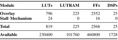
The proposed architecture can operate at maximum fre-quency of 770MHz, which is close to theoretical maximum, 775MHz, of the devices’s DSP blocks [13]. The resource utilization of each module is summarized in Table II. It is important to note that the design of the stall mechanism results in an insignificant area overhead, while the total utilization is very small, meaning this architecture could be scaled up significantly on this device.
TABLE II
RESOURCE UTILIZATION ON THEZYNQULTRASCALE+ ZU7EV.
Module LUTs LUTRAM FFs DSPs
Overlay 796 225 2552 25 Stall Mechanism 24 0 16 0
Total 819 225 2568 25
IV. RESULTS ANDDISCUSSION
From the simulations, we extracted the number of clock cycles for each network to process the first dataset entry, labelled latency, along with the clock cycles required to pro-cess a following entry when the pipeline is saturated, labelled interval. We also provide the number of stall cycles to quantify the stalling overhead. In each case we took into consideration the maximum operating frequency of 770MHz, showing how that translates to actual runtime in Table. III. Compared to other FPGA implementations in the literature, the authors in [11] implement a neural network for gas classification on a Xilinx Zynq XC7Z010T using Vivado HLS v2016.1. The architecture uses fixed point arithmetic and operates at 100MHz, as well as using the more expensive Sigmoid activation function. Parallelism is exploited with pragmas for loop unrolling and pipelining, and they report a latency of 540ns for their simpler 12-3-1 network topology, which is about 10× slower compared to the proposed overlay for a 8-12-8-1 network that results in a 48.026ns latency.
TABLE III
THEORETICAL TIMING RESULTS FOR THE OVERLAY.
Clock Cycles Time (ns)
Dataset Latency Interval Stall Latency Interval Stall
Customer Churn 32 11 0 41.536 14.278 0 Diabetes 37 12 4 48.026 15.576 5.192 Iris 35 10 6 45.43 12.98 7.788
To provide a reference for comparison we processed all three neural networks in software on the Arm Cortex-A53 bare-metal, operating at 1.2GHz, as found in the same Ul-trscale+ device. We also processed them on a desktop PC running Ubuntu Linux 18.04 on an Intel Core i7-6700 CPU, at 3.40GHz. Fixed point representation was used for the software, implemented in C. From the execution time measured and the theoretical timings of the overlay, we calculated the inference throughput for each network in Table. IV.
TABLE IV
INFERENCES PER SECOND ON THE DIFFERENT ARCHITECTURES.
Neural Network
Inferences/sec.
Arm-A53 @1.2 GHz
Core i7-6700 @3.40GHz
Overlay @770MHz
Customer Churn 0.151×10⁶ 3.618×10⁶ 70.04×10⁶ Diabetes 0.089×10⁶ 2.201×10⁶ 64.20×10⁶ Iris 0.099×10⁶ 1.29×10⁶ 77.04×10⁶
The proposed overlay offers a significant performance im-provement, compared to the embedded Arm core, able to process the networks in our case study at a significantly greater rate. The proposed overlay is at least 19× faster than the desktop class Intel Core i7-6700.
V. CONCLUSION
In this paper we presented a lightweight streaming neural network overlay that is optimised for the high performance
DSP blocks in modern FPGAs and exploits their programma-bility. The proposed overlay reduces dependency on the back-end toolflow and enhances flexibility and programmability of FPGAs in the neural networks domain. The implemented overlay architecture maintains low resource utilization while operating at near the theoretical maximum of the platform. The high operating frequency, that also contributes in minimising the impact of leakage current, coupled with the minimal resource utilization and significant performance improvements, make the proposed overlay ideal for processing at the edge.
In the future, we plan on expanding this work to support deeper and alternative neural network topologies along with a rapid toolflow to automate the configuration and mapping process. This will enable for rapid deployment of neural network accelerators on FPGAs at the edge in a context where compilation can take place on the resource constrained platforms themselves, independently of the vendor backend toolflow.
ACKNOWLEDGEMENT
This work was supported in part by an IBM Faculty Award and the UK Engineering and Physical Sciences Research Council (EPSRC), grant EP/N509796/1.
REFERENCES
[1] S. I. Venieris, A. Kouris, and C.-S. Bouganis, “Toolflows for mapping convolutional neural networks on FPGAs: A survey and future direc-tions,”ACM Comput. Surv., vol. 51, no. 3, pp. 56:1–56:39, 2018. [2] B. Ronak and S. A. Fahmy, “Mapping for maximum performance on
FPGA DSP blocks,”IEEE Transactions on Computer-Aided Design of
Integrated Circuits and Systems, vol. 35, no. 4, pp. 573–585, April 2016.
[3] E. Wu, X. Zhang, D. Berman, and I. Cho, “A high-throughput re-configurable processing array for neural networks,” in Proc. Field
Programmable Logic and Applications (FPL), Sep. 2017.
[4] A. K. Jain, D. L. Maskell, and S. A. Fahmy, “Throughput oriented FPGA overlays using DSP blocks,” in2016 Design, Automation Test in Europe
Conference Exhibition (DATE), March 2016, pp. 1628–1633.
[5] A. K. Jain, X. Li, P. Singhai, D. L. Maskell, and S. A. Fahmy, “DeCO: A DSP block based FPGA accelerator overlay with low overhead in-terconnect,” inProc. Field-Programmable Custom Computing Machines
(FCCM), 2016.
[6] J. Coole and G. Stitt, “Adjustable-cost overlays for runtime compila-tion,” in 2015 IEEE 23rd Annual International Symposium on
Field-Programmable Custom Computing Machines, May 2015, pp. 21–24.
[7] E. Wanget al., “Deep neural network approximation for custom hard-ware: Where we’ve been, where we’re going,”ACM Computing Surveys, vol. 52, no. 2, pp. 40:1–40:39, May 2019.
[8] I. Hubara, M. Courbariaux, D. Soudry, R. El-Yaniv, and Y. Bengio, “Bi-narized neural networks,” inAdvances in Neural Information Processing
Systems 29. Curran Associates, Inc., 2016, pp. 4107–4115.
[9] D. Sanvito, G. Siracusano, and R. Bifulco, “Can the network be the AI accelerator?” in Proc. Morning Workshop on In-Network Computing, ser. NetCompute ’18. New York, NY, USA: ACM, 2018, pp. 20–25. [10] M. Abadiet al., “TensorFlow: Large-scale machine learning on
heteroge-neous systems,” 2015. [Online]. Available: https://www.tensorflow.org/ [11] X. Zhai, A. A. S. Ali, A. Amira, and F. Bensaali, “MLP neural network
based gas classification system on Zynq SoC,”IEEE Access, vol. 4, pp. 8138–8146, 2016.
[12] S. Shreejith, B. Anshuman, and S. A. Fahmy, “Accelerated artificial neural networks on FPGA for fault detection in automotive systems,” in
Proc. Design, Automation Test in Europe Conference Exhibition (DATE),
2016, pp. 37–42.
[13] Zynq Ultrascale+ MPSoC Data Sheet: DC and AC Swithcing