Functional Materials
Jonathan Gratus1,2
E-mail:[email protected]
Paul Kinsler1,2
Rosa Letizia1,3
Taylor Boyd1,2
1Cockcroft Institute, Keckwick Lane, Daresbury, WA4 4AD, United Kingdom. 2Physics Department, Lancaster University, Lancaster LA1 4YB, United Kingdom. 3Engineering Department, Lancaster University, Lancaster LA1 4YW, United Kingdom.
Abstract.
1. Introduction
We show how we can use layered or varying material properties to sculpt an electric field profile along its propagation direction. Here we use sub-wavelength variation as a means of controlling the internal field profile [1, 2], in contrast to the typical uses of layered [3] or chirped [4] 1D photonic crystals, whose focus is primarily on manipulating the band structure, reflectivity, or transmission properties. Up to now most of the work has concentrated on photonic band gaps in photonic crystals, and the transmission or reflection coefficients at various angles or frequencies of an incident wave [5]. Our method is also distinct from the synthesis of optical waveforms by combining carefully phased harmonics [6, 7].
Many possibilities are unlocked by our ability to design field profiles with sub-wavelength customization. We might imagine enhancing ionization in high harmonic generation (HHG, see e.g. [8] and citations thereof), where the field profile aims to give a detailed control of the ionized electrons trajectory and recollision. Further, we might create localized peaks in the waveform, so that the concentration of optical power enhances the signal to noise ratio, or gives a larger nonlinear effect. Conversely, flatter profiles could help minimise unwanted nonlinear effects, or better localise the sign transition as happens for a square wave signal. In accelerator applications, there is much interest in controlling the size and/or shape of electron bunches (see e.g. [9]), or for pre-injection plasma ionisation for laser wakefield acceleration [10]; sculpted electric field profiles are one way of achieving the desired level of control.
Of course, when using customised field profiles to control an electron bunch in an accelerator or synchrotron, we need that field profile to be present in free space. We address this important case using a gap between two slabs of the necessary customised medium, and use CST Studio Suite [11] simulations of this arrangement to demonstrate that the desired field profile is still present within the slot. A slot also enables probes to be placed to measure the electric field, and can increase the transmission of external fields into the medium.
Here we consider the design of structures that perform this subwavelength field profile shaping. Because we are primarily discussing the basic principles rather than a specific application, we consider a variety of wavelength-scale unit cells designed to be joined together into a long multi-period waveguide structure. The result is a structure in which incident electromagnetic radiation of the correct frequency is transmitted to the far end, and whilst inside the structure it will have its field profile modulated as designed. Although when considering structures made of many unit cells, we restrict ourselves to periodic structures, this is merely for simplicity – if so desired, more complicated profiles could be designed.
(a)
−1
−1 4Λ
1 4Λ
1
˜
E
z
(b)
−1
−1 4Λ
1 4Λ
1
˜
E
[image:3.612.126.459.85.236.2]z
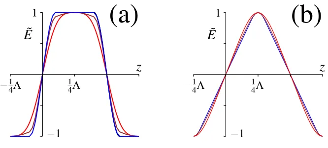
Figure 1.Field profiles for (a) the ‘flat-top’ wave structure withε(z)as defined in (5), where
`=Λ/10, and (b) the ‘triangular’ wave structure withε(z)as defined in (6), where`=Λ/10. In both cases we have not plotted the predicted field as it is coincident (at this resolution) to the simulated CST simulated field profile for ˜Ex(blue). The brown curve is the CST generated field profilein the slot, when a slot of16(flat-top) and13(triangular) width is cut in the structure; a good match is still achieved demonstrating that our scheme can also be used to control free-space field profiles. For comparison the Mathieu functions forn=1, andq=0.8 (flat-top) or
q=−0.329 (triangular) are plotted (red).
2. The permittivity function
To motivate our scheme we first consider assuming (or guessing) some promising dielectic functionε(z), and solving the wave equation forE(z)under those conditions, and varying the parameters to search for a suitable field profile. By selecting a simple material variation we could make use of existing solutions; notably repeating two-layer structure would allow us to repurpose work on (e.g.) Bragg reflectors. More interesting would be to assume a sinusoidal variation in permittivity, which has a wave equation that matches that for Mathieu functions‡ [12, 13]. The periodic Mathieu functions depend on two parametersan, q, wherean=an(q) is then-th characteristic value. These give solutions of the differential equation forAn,q(z)
∂z2An,q(z)−[an−2qcos(4πz/Λ)]An,q(z) =0. (1)
It is important to note thatΛis the wavelength of the electric field, which is exactly twice the length of the dielectric modulation. We see this 2:1 ratio between the periodΛ ofEand the period ofεr again below in the designed modes. Sample Mathieu functions, with parameters
chosen to give both flat-topped and triangular profiles are shown compared to other similar (but explicitly designed) profiles on fig. 1.
However, although Mathieu functions and the like are powerful sources of inspiration, we prefer to follow a design-lead scheme where we first specify the desired field profileE(z), then use the wave equation to calcuate what the position dependent dielectric propertiesε(z) needs to be. In principle this allows us to directly calculate the material function needed to support almost any electric field profile we might want.
Consider the single frequency transverse mode with E=eiωtE˜(z)i, P=eiωtP˜(z)i and
H=eiωtH˜(z)j, together with the permittivity
ε(ω,z) =ε0εr(ω,z)and vacuum permeability
µ0. Then Maxwell’s equations, where0=dzd, give
˜
E00+ω2c−2εr(ω,z)E˜=0,
so that εr(ω,z) =−c
2E˜00
ω2E˜
. (2)
In principle almost any electric field profile is possible. However, for some field profiles, the solution in (2) requires the presence of negative permittivity, possibly with a very high absolute value; in others ˆE00/Eˆ is undefined.
To simplify the discussion here we restrict ourselves to modes with odd symmetry about z=0 and z=Λ/2, and hence even symmetry about z=Λ/4 where Λ is the desired wavelength§. Thus
˜
E(z) =−E˜(−z) =−E˜(z+Λ
2) =E˜(z+Λ), (3)
and E˜(Λ
4 −z) =E˜(
Λ
4+z). (4)
Thus it is only necessary to specify ˜E(z)for 0<z<Λ/4. The symmetry requirements imply ˜
E(0) =0 and ˜E0(Λ/4) =0. From (4) and (2) one see thatεrhas period half that ofE, and has
even symmetry aboutz=0, i.e.εr(z) =εr(−z) =εr(z+Λ/2).
It is advantageous for the electric field to be composed of piecewise sections which are either sinusoidal, and hence correspond to constantεr, or linear, which correspond toεr=0.
Following this theoretical design step, we validate our scheme using 3D CST simulations based on a rod-like unit cell oriented alongz, with a nearly square cross section inx andy; the cell shape can be seen in fig. 2. On thexboundary we set a perfect magnetic conductor (i.e. Htrans=0), and on theyboundary we have a perfect electric conductor (i.e. Etrans=0).
Thezboundary conditions are periodic with a phase shift of 180◦. We choose these boundary conditions since if we instead used all periodic conditions, then spurious modes with finiteky orkz transverse to the variation (inz) would appear.
3. Wave Profiles
In this work we confine ourselves to consider only material variation that has a strictly positive-valued permittivity everywhere. In part, this is because materials with negative permittivity are typically strongly dispersive, and so there may be – at the very least – stringent bandwidth limitations. With this constraint, and for some choices of profile, it can be more difficult to construct the permittivity function that supports an electric field with sufficient accuracy.
§ We can also go further and choose our permittivity function so thatεr>0, and thatεrdoes not change rapidly.
? ?? ?
? ?? ??
?
666
66 6
6 66 6 ? ?? ?
? ?? ??
? 66
66 6
6 66 6 6
[image:5.612.152.416.97.214.2]−1E˜ 0 1 x field
Figure 2.Results from 3D CST models of the unit cells for the ‘flat-top’ (top) and ‘triangular’ (bottom) wave structure including free-space slots as described in fig. 1, showing the electric field strength and direction through the structure. In both cases the field in the slot differs from the field in the structure by less than 1%.
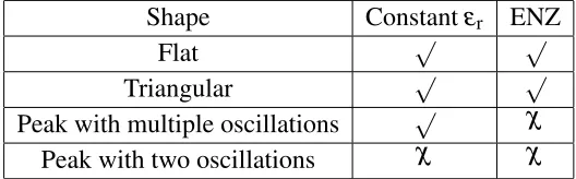
Nevertheless, by using materials with very low permittivityε (epsilon near zero, ENZ), one can construct profiles which are (e.g.) almost flat for a significant proportion of the mode, or which have near constant gradient – both being shown in fig. 1. These profiles were inspired by Mathieu functions of similar appearance, but as we found, that general appearance does not require the specific sinusoidalεvariation needed for the Mathieu functions themselves. In addition, profiles with strongly localised peaks can be achieved by combining two materials of significantly different permittivities, and if one is prepared to tolerate less precise profiles, it may be possible to construct reasonable flat-top and triangular profiles using only materials withε ≥1. For brevity, here we will consider only the four representative profiles indicated in table 1. The first three permittivity functions are all step-like, consisting of one high index and one low-index region.
Shape Constantεr ENZ
Flat √ √
Triangular √ √
Peak with multiple oscillations √ χ
Peak with two oscillations χ χ
Table 1. The four electric field profiles considered in this article, and the permittivity properties required to generate them.
3.1. Flat-top wave profile
[image:5.612.162.426.498.580.2]harmonic components would require a significant effort, especially if attempting to build an optical square wave (see e.g. [6]). However, using our technique we can sidestep that effort by constructing instead a designer functional material that quite naturally supports such waveforms. We can generate our flat-top wave profile using
˜ E(z) =
(
sin(πz/2`), 0<z< `
1, ` <z< 14Λ,
and εr(z) =
(
c2π2/4`2ω2, 0<z< `
0, ` <z< 14Λ,
(5)
for`, with 0< ` < 14Λ. We implemented this structure in CST, based on a unit cell with cross sectionax=6mm,ay=6.22mm, and lengthsΛ=52mm,`=5.2mm. The slot, when present, was 1mm wide. Fig. 1 demonstrates that the designed-for field profile is achievable even in a 3D simulation; a 3D visualization is given in fig. 2.
3.2. Triangular wave profile
A field profile with a triangular form, just like a square wave or indeed any waveform can be synthesized from its harmonics. In comparison to the square wave in particular, though, the proportion of higher harmonics falls off more rapidly, so any synthesis would in practice be easier. This ramped field profile could also be used to impart a well-managed linear chirp to charged particles in a bunch.
Nevertheless, here we can design a structure which naturally supports triangular waves, which is given by
˜ E(z) =
(
ksin(k`−14kΛ)z, 0<z< ` cos(kz−14kΛ), ` <z< 14Λ,
and εr(z) =
(
0, 0<z< `
c2k2/ω2, ` <z< 14Λ,
(6)
where `, with 0< ` < 14Λ, and let k>0 be the lowest solution to `k=cot(14Λk−`k). We implemented this structure in CST, based on the same unit cell as for the flat-top wave; except that when present the slot width was 2mm. Fig. 1 demonstrates that the designed-for field profile is achievable even in a full 3D simulation. A 3D visualization is given in fig. 2.
1
˜
E
−
1
1 4
Λ
z
[image:7.612.196.386.90.272.2]−
14Λ
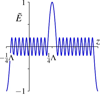
Figure 3. Field profiles for the the ‘multi-oscillation wave’ structure withε(z)as defined in
(7),`= (0.8)41Λandn=5. The CST simulated field profile for ˜Ex(blue) is nearly coincident
with the designed-for profile from (7).
3.3. Peaked profile with multiple oscillations
Waveforms with strongly localized peaks can also be useful, particularly where an amplitude and/or intensity threshold is the chosen discriminator. However, just like any wave with distinct or localized features, they have a significant harmonic content and we might therefore prefer not to synthesize them directly. Unfortunately, as we have noted, long intervals of a near-constant electric field in a waveform require very small permittivity values (i.e. the ENZ regime). To avoid this complication, we might replace an idealized near-constant region with many low-amplitude rapid oscillations that are assumed to cycle-average to zero.
In the range 0 < z< ` there is a small ˜E(z) with n oscillations, whereas the range ` <z<14Λprovides the desired single large oscillation. The profile is chosen so that ˜E(`) =0, so that
˜ E(z) =
`sin(2nπz/`) 4n(14Λ−`)
, 0<z< `
cos
"
π(14Λ−z) 2(14Λ−`)
#
, ` <z< 14Λ,
and εr(z) =
(
4c2n2π2/ω2`2, 0<z< `
c2π2/4ω2 14Λ−`2, ` <z< 14Λ.
(7)
This theoretically designed waveform is shown in fig. 3, along with that resulting from 3D numerical simulations using CST.
3.4. Peaked profile with two oscillations
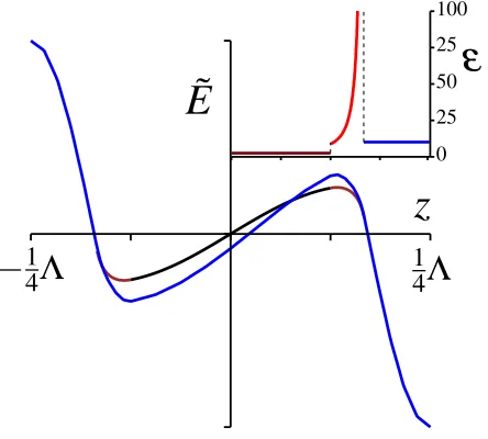
−
14Λ
˜
E
1 4
Λ
z
50
0 25
25 100
[image:8.612.183.405.90.290.2]ε
Figure 4.Field profiles for the the two-oscillations structure. The CST simulated field profile for ˜Ex(blue) is broadly similar but not that well matched to the designed-for profile from (8),
with its constantε(black) and quadratic Bezier (red) parts. This is becauseεrnot only needs
to be very large for a very thin slice, but is also rapidly varying. The structure has aε(z)from (8), with`0=0.5(12Λ),`1=0.668(12Λ),λ0=0.5,λ1=2.0,k0=2.5/(21Λ)andk2=5/(12Λ); where the quadratic Bezier, is is given parametrically byz= (−0.049t2+.132t+.25)Λand
˜
Ez=−.401t2+.105t+.474
something closer to the design goalcanbe made if we construct an ˜E(z)using two sinusoidal regions and a quadratic Bezierkfunction B(z) to interpolate between them. Withεr(z)from
(2), this profile is
˜ E(z) =
λ0sin(k0z), 0 <z< `0
Quadratic-Bezier, `0<z< `1
λ1sin(k1z), `1<z< 14Λ.
(8)
For this construction the challenge now becomes that the permittivity becomes very large in a small region; the required εr can be seen in the inset of fig. 4. Further, even before
any difficulties of fabricating an experimental structure are considered, generating numerical results for this is problematic. We therefore split the smooth part of the ε profile with its extreme values into a set of thin layers, the thinnest layer havingε =1262 (i.e. a refractive index ofn≈36). Using this approximate implementation, we can see in fig. 4 the results of using CST to generate a field profile in comparison to the designed-for wave shape – there are significant regions where the match is relatively poor. Nevertheless, the general character of the desired wave profile is achieved, and the important high-field peaksareclosely matched.
0 1 2 3 4 5 6
Frequenc
y
(GHz)
0◦ 45◦ 90◦ 135◦180◦
Transm. Coeff.
[image:9.612.156.428.88.252.2]0 0.5 1
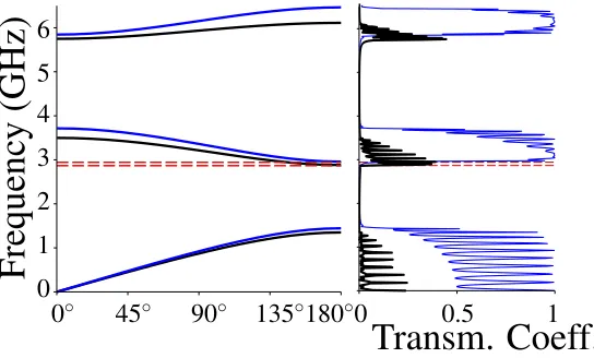
Figure 5.Bandstructure (left) for the unit cell of the flat-top structure; and transmission (right) for a 3D ten cell version. The results shown are calculated using CST, both without (black) and with (blue) the presence of a slot. The angle gives the phase difference across the length of the unit cell. The operating frequencies (dashed lines) are at a 180◦phase shift. Without a slot the frequency is 2.867GHz & 30% transmission (red), and with a slot it is 2.911GHz & 95% (brown). Transmission data was obtained by exciting the structure with a Gaussian pulse of width 52.5ps and time delay 0.1367 ns, and taking results after 60ns of simulated time.
4. Practical Issues
Having first considered very idealized structures that assume an infinite number of periods, we now move to the finite structures of the kind most likely to be built. We have already demonstrated one practical feature of our scheme – the free space field wave profile shaping using a slot. This leaves several important issues to be considered: (i) whether an incident field will penetrate efficiently into the structure for modulation, (ii) the effect of material losses, (iii) and to what extent will the profile shaping persist in the non-idealized case.
First, since the structural periodicity is a good match to the incident wavelength, any devicemightbe expected to act more like a Bragg mirror, with or without a slot. Consequently, we adapted our CST simulations to also treat finite-period structures. The left hand panel of fig. 5 shows a comparision of the bandstructures for a single cell structure, with and without a slot. We can easily see that the character of the bandstructures is preserved and that the slot-induced upward frequency shift is relatively small. This trend was repeated in CST simulations for our other slotted structures. Further, on the right hand panel of fig. 5, we see the transmission spectrum for 10 period structures with and without a slot. As a direct result of our design process, we see that the presence of a slot – and perhaps despite its sub-wavelength width – enhances transmission into the structure.
Transm. Coeff.
[image:10.612.160.429.89.310.2]Frequency (GHz)
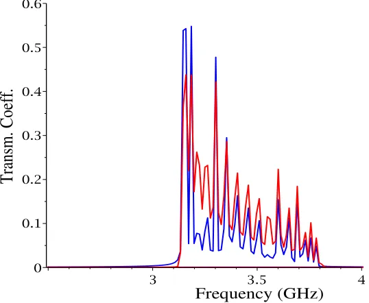
Figure 6. Relevant part of the transmission spectra for the CST simulations with loss. The weakly damped case withγw=2.6×10⁶s−1is shown using a blue line, whereas the medium
damped case withγm=10.4×10⁶s−1is shown using a red line. We also fitted the CST time
series data using a set of decaying exponentials as implemented by the open source Harminv software [15, 16]. The spectral response as reconstructed from the fitting process was in good agreement with the location of the transmission peaks shown here.
hours. The losses were specifed by adding an imaginary contribution to the permittivity of each slab in the stack, values which CST used to generate an appropriate response model for its simulations. We primarily investigated three cases, which correspond to no damping, weak damping, and medium damping. The no damping case used a low permittivity slab with εn,1/ε0=10−4 and a high permittivity slab with εn,2/ε0=62500×10−4. The weak
damping case used a low permittivity slab with εw,1/ε0 = (1+0.1ı)×10−4 and a high
permittivity slab with εw,2/ε0= (62500+62.5ı)×10−4. The medium damping case used
a εs,1/ε0= (1+62.5ı)×10−4 but the same εs,2. The scale factor of 10−4 for each of these
was removed in the CST simulations to assist with the numerical calculations, but of course the simulation output then required a compensating rescaling.
The different loss properties of the low and high permittivity slabs mean that the overall loss is some combination of the individual contributions. We therefore obtained the net loss coefficientγ of the structures from the energy loss rate of our time domain simulations. The simulations showed that for weak losses we had that γw = 2.6×10⁶s−1 and for medium losses we found that γm = 10.4×10⁶s−1. However, as we can see on fig. 6, although the two cases gave different transmission spectra, the qualitative character of the two was preserved. However if we went to “extreme” damping by setting the low permittivity slab to
εe,1/ε0= (1+625ı)×10−4, then this gave a net loss ofγe=19×106/s, which was sufficient to destroy the desired character of our results.
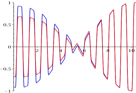
Figure 7. Typical flat-top mode profiles from the time domain simulations in fig. 6, as extracted using CST field monitors at 3.1457GHz. The horizontal axis is scaled to unit cell lengths, and shows the entire 10 period wave structure. The wave profile for the weakly damped case is shown using blue lines, and for medium damping using red lines. We can see in these results that significant profile sculpting of the type designed for has been achieved.
frequencies. Note that in a lossless structure, if the chosen frequency is slightly below the band edge, the incident field will decay with penetration distance inside the structure, although if less than critically damped, the field profile will still have the designed-in modulation (e.g. flat topped), but modulated by a decaying exponential. If the chosen frequency is above the band edge, the designed wave profile will instead be subject to a sinusoidal modulation of the envelope. This means that we want to drive as close to the band edge as possible; but with losses and a finite structure there no longer is a sharp well-defined band edge to choose; however there is a cut-off in the transmission spectrum which on fig. 6 occurs slightly above 3.1GHz. Nevertheless, our time domain simulations do show that field mode profile customization is possible, with results shown on fig. 7. Our expectation is that the envelope modulation could be further minimised by either adjusting the driving frequency, or using a structure with more cells. However, due to the intensive computational requirements, this optimization might be better explored in an experimental setting along with the other practical considerations, rather than in simulation.
5. Conclusions
profiling can be achieved in free-space by means of a slotted structure, and that the desired field modes inside the structure can be excited, even in the presence of loss and finite length.
In future work we aim to investigate more realistic models of our structures. The applications in electron beam control that we forsee are in the RF or microwave regime, where sub-wavelength fabrication is relatively easy. Nevertheless, metamaterial fabrication techniques are now routinely being pushed through the THz regime and towards the optical. This is driven in large part by the opportunities made available by transformation optics design [17]: consider for example the infrared Luneburg lens [18].
Note that although in several figures we have chosen length scales of millimeters and a frequency regime in the GHz, the general electromagnetic approach we have used applies, or can be rescaled, to either longer or shorter wavelengths. Further, it seems likely that this scheme can be adapted to other fields such as acoustics.
Acknowledgements
The authors are grateful for the support provided by STFC (the Cockcroft Institute ST/G008248/1 and ST/P002056/1) and EPSRC (the Alpha-X project EP/J018171/1 and EP/N028694/1).
References
[1] Gratus J, McCormack M and Letizia R 2015
Proceedings of PIERS 2015 in Prague675–680
URLhttp://piers.org/piersproceedings/piers2015PragueProc.php%3Fstart=100
[2] Gratus J and McCormack M 2015
J. Opt.17025105 (Preprint1503.06131)
URLhttp://dx.doi.org/10.1088/2040-8978/17/2/025105
[3] Russell P S J, Birks T A and Lloyd-Lucas F D 1995
Photonic bloch waves and photonic band gaps Confined Electrons and Photons: New Physics and Applications(NATO Advanced Science Institutes Series Bvol 340) ed Burstein E and Weisbuch C pp 585–633 conference: NATO Advanced Study Institute on Confined Electrons and Photons - New Physics and Applications, (Springer, Boston MA)
URLhttp://link.springer.com/chapter/10.1007/978-1-4615-1963-8%5F19
[4] Russell P S and Birks T A 1999
J. Lightwave Techn.171982–1988
URLhttp://dx.doi.org/10.1109/50.802984
[5] Joannopoulos J D, Johnson S G, Winn J N and Meade R D 2011
Photonic crystals: molding the flow of light(Princeton University Press, Princeton MA) [6] Chan H S, Hsieh Z M, Liang W H, Kung A H, Lee C K, Lai C J, Pan R P and Peng L H 2011
Science3311165–1168
URLhttp://dx.doi.org/10.1126/science.1198397
[7] Cox J A, Putnam W P, Sell A, Leitenstorfer A and K¨artner F X 2012
Opt. Lett.373579–3581
URLhttp://dx.doi.org/10.1364/OL.37.003579
[8] Radnor S B P, Chipperfield L E, Kinsler P and New G H C 2008
(Preprint0803.3597)
URLhttp://dx.doi.org/10.1103/PhysRevA.77.033806
[9] Piot P, Sun Y E, Power J G and Rihaoui M 2011
Phys. Rev. ST Accel. Beams14022801 (Preprint1007.4499)
URLhttp://dx.doi.org/10.1103/PhysRevSTAB.14.022801
[10] Albert F, Thomas A G R, Mangles S P D, Banerjee S, Corde S, Flacco A, Litos M, Neely D, Vieira J and Najmudin Z 2014
Plasma Physics and Controlled Fusion56084015
URLhttp://dx.doi.org/10.1088/0741-3335/56/8/084015
[11] CST AG,
CST Studio Suite
URLhttp://www.cst.com/
[12] El Haddad A 2016
Optik1271627–1629
URLhttp://dx.doi.org/10.1016/j.ijleo.2015.11.049
[13] Gratus J, Kinsler P, Letizia R and Boyd T 2017
Appl. Phys. A123108
URLhttp://dx.doi.org/10.1007/s00339-016-0649-8
[14] Kohler M C, Pfeifer T, Hatsagortsyan K Z and Keitel C H 2012 Frontiers of atomic high-harmonic generation
Advances In Atomic Molecular and Optical Physics, Volume 61
(Advances In Atomic Molecular and Optical Physicsvol 61) ed Arimondo E, Berman P R and Lin C C (Elsevier) pp 159–208
URLhttp://dx.doi.org/10.1016/B978-0-12-396482-3.00004-1
[15] Mandelshtam V A 2001
Progress in Nuclear Magnetic Resonance Spectroscopy38159–196
URLhttp://dx.doi.org/10.1016/S0079-6565(00)00032-7
[16] Johnson S G Harminv
URLhttp://ab-initio.mit.edu/wiki/index.php/Harminv
[17] Kinsler P and McCall M W 2015
Photon. Nanostruct. Fundam. Appl.1510–23
URLhttp://dx.doi.org/10.1016/j.photonics.2015.04.005
[18] Zhao Y Y, Zhang Y L, Zheng M L, Dong X Z, Duan X M and Zhao Z S 2016
Laser and Photonics Reviews10665–672