University of Warwick institutional repository:http://go.warwick.ac.uk/wrap
A Thesis Submitted for the Degree of PhD at the University of Warwick
http://go.warwick.ac.uk/wrap/73129
This thesis is made available online and is protected by original copyright. Please scroll down to view the document itself.
A Metrological
Scanning force microscope
YingXu
(M.Se, B.Se)
Submitted for the degree of Doctor of Philosophy
to the Higher Degrees Commttee
University of Warwick
Centre for Nanotechnology and Microengineering
Department of Engineering' . '. " '
University of Warwick, Coventry; U.K.
.. .. ... "~:>:'"
March
1995~"
./ /:\j">'/ ::.)
~-IMAGING SERVICES NORTH
Boston Spa, WetherbyWest Yorkshire, LS23 7BQ www.bl.uk
BEST COpy AVAILABLE.
',.
VARIABLE PRINT QUALITY
Abstract
In last decade, there has been a tremendous progress in scanning probe
micro-scopies, some of which have achieved atomic resolution. However, there still exist some problems which have to be solved before the instrument can be used as
a metrological measurement tool. The object of the project introduced in this
thesis was to develop a scanning force microscope of metrological capability with the aim of making significant improvement in scanning force microscopy from the
viewpoint of instrumentation.
A capacitance based force probe has been studied theoretically and
experi-mentally with the main concern being its dynamic properties, characterized by
squeeze air film damping, which are believed to have direct effects on the fidelity
of measurement. The optimization of design is investigated so as to achieve the
results of both high displacement sensitivity and force sensitivity.
An x-y scanning stage has been designed and built, which consists of a two axis linear flexure system of motion amplifying mode machined from a single
aluminium alloy block. The stage is driven by two piezo actuators with two
ca-pacitance sensors monitoring the actual position of the platform to form a closed
loop control system. The design strategy is introduced and the performances and
characteristics of two commonly used types of flexure translation mechanisms, leaf
spring and notch hinge spring system, are analyzed. The finite element analysis
method is employed in the analysis and design of translation mechanism. Finally, a metrological scanning force microscope has been constructed,
com-bining a constant force probe system, an x-y scanning stage and a 3D coarse positioning mechanism into a metrological system. The performance of the
in-strument system has been systematically evaluated and its measuring capability
investigated on the. specimens of various properties and features. The results from
\
this first prototype of the instrument demonstrated a subnanometer resolution
Acknowledgment
I would like to take this opportunity to express my sincere gratitude to Dr S.T. Smith, my supervisor, for his continual support and encouragement, without
which this project would not have been possible. His effort in improving my ,
academic writkg skill is also appreciated.
My sincere thanks to Professor D.K. Bowen, my supervisor at the later stage
of my Ph.D course, for his effective supervision and help in the process of writing
up the thesis. I like his dynamic working style.
Thanks also go to Dr. D.G. Chetwynd for his help and useful advices on my
project, and to Dr. X. Liu for her help in my laboratory work.
Thanks to the technicians at the Centre for Nanotechnology and
Microengi-neering: Steve, Dave, Rhod and Frank for their careful craftsmanship and
friend-ship.
The Queensgate 'Instruments Ltd. is to be thanked for the cooperation of
building the precision X-Y scanning stage and providing experiment facilities.
Finally, I am very grateful to Chinese government, British government and
Sir. Y.K. Pac for a Sino-British Friendship Scholarship which supported my
Declaration
This thesis is presented in accordance with the regulations for the degree
Contents
1 Introduction
1.1 Surface metrology in engineering . 1.2 Instrumentation for surface metrology.
1.2.1 Stylus instruments
1.2.2 Optical methods .
1.2.3 Modern scanning microscopies .
2 Development of scanning probe microscopes 2.1 Scanning probe microscopy. . . .
. 2.1.1 Scanning tunneling microscopy
2.1.2 Scanning force microscopy . . .
2.1.3 Scanning near-field optical microscopy
2.1.4 Scanning capacitance microscopy
2.1.5 Scanning thermal microscopy 2.2 SFM transduction methods . . . .
2.2.1
2.2.2
2.2.3
2.2.4
Tunneling detection system Capacitance detection system
Optical detection system . . . .
2.2.3.1 Optical beam deflection
2.2.3.2 Laser-diode feedback detection
CONTENTS
2.3 Scanning and coarse positioning mechanism
2.3.1 Scanning mechanism . . . . .
2.3.1.1 Piezoelectric tripod.
2.3.1.2 Tube scanner . . .
2.3.1.3 Bimorph scanner
2.3.1.4 Piezo-flexllre stage
2.3.2 Coarse positioning mechanism .
2.3.2.1 Inchworm . . . 2.3.2.2 Piezo-walker 2.3.2.3 Magnetic walker
2.3.2.4 Inertial glider . . .
2.3.2.5 Screw-driven mechanism .
3 Force probe system
.
.
3.1 Introduction . . .
· . .
.
.
.
. .
.
.
.
.
. . .
. .
.
.
.
. . .
.
.
.
.
ii 37 37 38 38 40 41· 42 43 43 45 46 47 58 583.2 Effects of damping on surface measurement with stylus method . 60 3.3 Dynamic characteristics of the force probe: theoretical analysis . 63
3.4 Experimental assessment of the theoretical model . 73
3.5 Parameter design . . .
3.5.1 Introduction . . 3.5.2 Mathematical model
3.5.3 Determination of optimal parameters
3.6 Fabrication of the force probe
3.7 Force probe system
3.7.1 Linearity ..
3.7.2 Constant force probe system. 3.8 Conclusion . . . .
·
. .
.
.
.
.
. .
.
. .
4 Precision X-Y stage
CONTENTS 111
4.2
Flexure translation mechanisms..
104
4.2.1
Stiffness..
"...
105
4.2.2
Deflection range . .108
4.2.3
Parasitic deflection errors· ....
110
4.2.3.1
Effect of driving force110
4.2.3.2
Effect of manufacture115
4.2.4
Compound rectilinear mechanisms.· .
. .
.
118
4.2.5
Two dimensional rectilinear mechanisms119
4.3
Design of precision X-V scanning stage for SPM124
4.3.1
Introduction . . .124
4.3.2
Description of the X-Y stage . .124
4.3.3
Some problems in the design . .127
4.3.4
Dynamic modelling . • . . .·
".
. .
130
4.3.5
Experimental assessment of motion errors132
4.3.6
Finite element analysis . . .135
4.3.6.1
Geometrical model building and mesh generation135
4.3.6.2
Boundary condition definition.136
4.3.6.3
Static deflections .138
4.3.6.4
Dynamic solution .146
4.4
Discussion and conclusion...
148
5 Metrological SFM system 153
5.1
Introduction . . .153
5.2
Principle of operation.154
5.3
Some design details . .158
5.3.1
X-Y axis coarse positioning mechanism .158
5.3.2
Probe coarse approach mechanism. . .161
~:
5.3.3
Measurement loop and material selection .162
5.3.4
Electronic specification163
CONTENTS iv
5.4.1
Instrument calibration.
166
5.4.2
Noise level . . .171
5.4.3
Stability and repeatability174
6 Surface measurement 183
6.1
Surface topography.
. . .
. . .
183
6.2
Surface roughness measurement192
6.2.1
Introduction . . .192
6.2.2
Instrumentation . .193
6.2.3
Experiment process and results. . . .
.
195
6.2.4
Discussion . . .199
6.3
Discussion and conclusion200
7 General discussion and conclusion 204
7.1
Metrological issues204
7.2
What is measured .206
7.3
Further improvement on X-Y stage208
7.4
Conclusion . . .210
A Program for force probe design
212
List of Tables
3.1 The calculated values of ch3 / p. vs I & b • • • . • • . . • • . 72
3.2 The comparison of the results of experiment and calculation 76 3.3 Damping ratio errors caused by parameter errors . . . 80 3.4 The parameters versus properties of the probe (ho = 4, 5p.m) 85 3.5 The parameters versus properties of the probe (ho = 6,8p.m) 86
3.6 The pe.rameters versus properties of the probe (ho = 10p.m) 87
3.7 The nonlinear errors of the capacitance probe • . . . 95
4.1 Parasitic pitching errors caused by driving forces (from mathe-matic models) . . . 112 4.2 Parasitic pitching errors caused by driving forces (from FEA models) 112
4.3 Rotation error of a simple flexure caused by non-parallel
arrange-ment of parallel hinges . . . 118
4.4 Measured results for angular errors of the x-y stage 4.5 The parameters chosen for element size setting ..
4.6 The results of static solution of FEA . . . . . .
134
136
139
6.1 Results of the measurements by Nanostep, SFM and GIXR . 197
List of Figures
1.1 Block diagram of relationship between surface measurement,
man-ufacturing and function. . . .
1.2 Schematic diagram of typical stylus instrument 1.3 Schematic diagram of stylus datum systems . . . 1.4 Optical arrangement of Foucault knife-edge follower
1.5 Interferometer for surface metrology. (a) Interference fringes, (b)
Fizeau interferometer . . . .
1.6 Schematic arrangement of X-ray reflectometry
1. 7 Schematic diagram of an SEM . . . .
2.1 Schametic diagram of the configuration of atomic scanning
micro-scope . . . .
2.2 The plot of interatomic force . .
2.3 Schematic diagram of tunneling detection system
2 4 5 6 8 9 11 20 21 26 2.4 Schematic diagram of capacitance detection system 28
2.5 Schematic diagram of electrostatic force balanced force probe. 29 2.6 Schematic diagram of a high stiff tribological force probe . . . 30
2.7 Schematic diagram of optical beam deflection detection system . . 32
2.8 Schematic diagram of laser-diode feedback detection system 34 2.9 Schematic diagram of homodyne detection system. . . 35
1.
2.10 Schematic diagram of fiber-optic interferometer detection system. 36 2.11 Schematic diagram of piezoelectric tripod scanning mechanism.. 39
2.12 Schema.tic diagram of tube scan.ner VI
LIST OF FIGURES vii
2.13 Bendiug mode of tube scanner. (a) Simple bending, (b) S-shape
bendillg .. . . . 40
2.14 Scherrlatic diagram of bimorphscanner . . . 41 2.15 Schematic diagram of piezo-flexure stage, (From reference 59) 42
2.16 Operation principle of inchworm. (a) The inchworm is ready for a
new st~p. piezo 1 clamps. (b) Piezo 2 expands. (c) Piezo 3 clamps
and Piezo 1 releases. (d) Piezo 2 contracts, and the tube is moving
up. . . . 44 2.17 Schematic diagram of operation principle of piezo-walker 45
2.18 Schematic diagram of magnetic walker 46
2.19 Schematic diagram of ineltial glider. . . 47 2.20 Schematic diagram of a differential spring reduced screw positioner 48
3.1 The force probe
. . .
.
.
. . .
. .
.
. .
. .
.
.
.
. .
. . .
.
3.2 Schematic diagram of simplified model of general stylus method . 3.3 Surface spectrum weighting factors for different damping system(after reference 5) . . . . 3.4 Modeling parameters of the force probe . .
3.5 Beam model satisfying the boundary condition of zero flow at the
clamped end and ambient pressure at the beam edge
...
3.6 The distribution of the damping pressure along central axis of a
cantilever beam, b
=
1.5 mm,Vo
=
1 mm8-1,
h=
15 p.m . . . . .3.7 The relationship between damping ratio and gap for a variety of
lengths of a glass (E
=
70QPa) cantilever with the dimension b=
1.5 mm, t
=
0.1 mm and tip mass mt=
2mg • . . • • . • • . • • .3.8 The r,:;lationship between damping factor and cantilever geometry 3.9 The so::hematical diagram of the dynamic testing system .
3.10 The me~ured transfer function of the force probe . 3.11 The measured coherence function of the force probe
3.12 The measured transfer function of over damped force probe.
LIST OF FIGURES
viii
3.13 The comparison of the results of experiment and calculation. x -~~,
+ -
{c, 0 -et .. . . ..
773.14 Calculated damping forces using different deflection models, (a)
results, (b) difference between the two theoretical models
3.15 The comparison of the profiles of two deflection models
3.16 The curve of etching depth against etching time . . . .
3.17 The diagram of the pattern of aluminium layer deposited on base 78 79
89·
blocl( . . . .. 89
3.18 Schematic diagram of cantilever machining using milling machine 90 3.19 Plot of the output of capacitance C / K(K = lbe:) versus the
deflec-tion of cantilever tlh, (ho = lOpm), from equation (3.29) . . . 93 3.20 Plot of the linearity error against the capacitance gap thickness ho
with the same deflection range of 2 pm . . . .. 93
3.21 Plot of the linearity error against the thickness of capacitance gap ho corresponding to relative deflection ranges of 20
%
and 30% .
94 3.22 The Curve of the output of probe versus the relative displacementbetwe€:n the probe and surface . . . .. 95
3.23 Schematic diagram of constant force servo system of the force probe 97
3.24 The diagram of the constant force profiling system. . 97
3.25 Profile of a single diamond turned silicon surface. . . . 99
4.1 The diagram of simple flexure rectilinear mechanisms
4.2 The configurations of the flexure springs
4.3 Plot of Q in equation (4.10) against
R/t
4.4 Simple parallel movement of leaf spring system: (a) undeflected, 106
107
109
(b) intended parallel deflexion, (c) undesired deflexion. . . 111
4.5 FEA model of leaf spring and its solution. (a) FEA model -deformed and un-deformed, (b) Pitching curve of moving platform
LIST OF FIGURES
4.6 FEA model of hinge spring and its solution. (a) FEA model -deformed and un-deformed, (b) Pitching curve of moving platform
ix
a-b. . . 114
4.7 Deflexion from parallelism of motion caused by manufacturing errors 11 7
4.8 Schematic diagram of compound rectilinear mechanism . . . '. 120
4.9 Schematic diagram of double compound rectilinear mechanism 120·
4.10 Schematic diagram of a symmetric rectilinear system of three-hol<~/1 wo-web flexure elements . . . 121
4.11 Schematic diagram of a symmetric rectilinear system double leaf spring flexures. . . 121
4.12 Schematic diagram of two dimension rectilinear mechanism. . 123
4.13 Schematic diagram of configuration of 8220 x-y scanning stage. . 125 4.14 Schematic diagram of translation configur~tion of the x-y scanning
stage . . . . 126 4.15 Schematic diagram of a simple model of motion amplification
mech-anism for effective stiffness analysis . . . 129 4.16 The schematic diagram of spring systems on the x and y axes. (a)
Model for the x axis, (b) Model for the y axis . . . . . 130 4.17 The relationship between natural frequency and mass added on
the platform.
.
.
. . . .
.
. . .
. .
.
. .
.
.
. . .
.
. . . 133
4.18 The schematic diagram of angular error measurement setup for measuring the yaw and pitch errors of the x axis and the roll error
of the y axis . . . . 134 4.19 Diagra.'ll of meshed model for x-y stage (S220) 137 4.20 Diagram of boundary condition for FEA model 138 4.21 Deformed models from FEA static solution. (a) the stage is driven
LIST OF FIGURES x
4.24 Distortion curve of nodes along c-d, (Model-A) . . . 143 4.25 Distortion curve of nodes along j-k, (Model-A). . . 143 4.26 The yaw error of platform in the x axis (Model-B) . 144
4.27 Distortion curve of nodes along a-b, (Model-B) . . . 144 4.28 Distortion curve of nodes along c-d, (Model-B) .. : 145 4.29 Distortion curve of nodes hlong j-k, (Model-B) . . 145·
4.30 Free vibration mode of the stage, (mode-I) . . 147
4.31 Free vibration mode of the stage, (mode-2) . . 147 4.32 Free vibration mode of the stage, (mode-3) . . 148
5.1 Block diagram of SFM system. 155
5.2 Photograph of the SFM system 156
5.3 Isometric sketch of the metrological SFM . . 158
5.4 Isometric sketch of the X-V coarse positioning mechanism 159 5.5 Section view of y axis locking mechanism. . . 160 5.6 Diagram of elastic contact mechanism of Z translator carriage 161
5.7 Diagram of decoupling mechanism. . . 162
5.8 Schematic diagram of the measurement loop of the instrument 164 5.9 Schematic diagram of S2000 rack system . . . . . 165
5.10 Block diagram of of SM Servo Module . . 166
5.11 Schematic diagram of calibration system of the x-y stage 168 5.12 Plot of the calibration curves of the X-Y stage in x axis. . 168 5.13 Schematic diagram of calibration set for measurement system in
the z axis . . . 169
5.14 Plot of the calibration curves of measurement loop in the z axis . 170 5.15 Plot of standard step profiles from SFM and Nanostep 170
5.16 Noise level of the instrument system . . . 171
5.17 Noise
le~el
corresponding to sampling processes with various av-eraging times for each data point. The avav-eraging times for theseLIST OF FIGURES Xl
5.18 Noise level and speed of data acquisition vs. averaging times ~ . . 173
5.19 Noise levels of x-y scanning stage in the x axis. (a) - open-loop control state, (b) - closed-loop control state.
5.20 Plots of system thermal drift. . . .
5.21 Ramp scan trace for analysis of linearity 5.22 Plots of two meander pattern scans . . . .
5.23 Plot of two optical grating surface profiles obtained from a
contin-uous forward and backward scan . . . .
...
6.1 SEM image of normal stylus tip of radius 1 p.m
6.2 SEM image of Berkovich tip of radius
<
0.1 p.m6.3 Image of optical grating surface. (a) 3D view, (b) Section profile
6.4 2D view of the same grating surface as in Fig.6.3
...
6.5 SEM image of the same grating surface as in Fig.6.3 ..6.6 SPM image of standard gratings of 2160 lines/mm for SEM
cali-bratioL . . . .
6.7 SPM image of polymer film (D9)
6.8 SPM image of polymer film (D12) .
6.9 SPM image of polymer film (D2) .
...
6.10 SPM image of a well polished Zerodur optical flat
175 176 177 179 179 184 184 187 188 188 189 189 190 190 191 6.11 3D image of electronic components on a silicon chip . 191
6.12 Surface topography of Sd Sio.sGeO.2/ Si heterostructure sample 192 6.13 Calcula.ted GIXR of a perfect smooth surface and the surfaces with
added roughness. . . 194
6.14 Curve of a specular scan from the GXR1 reflectometer 198
6.15 SFM image of Surface topography of Zerodur 4/1 . . . 199
7.1 The interaction forces between a diamond tip and a floating glass
"t
cleaned with Acetone . . . . 7.2 Schematic diagram of piezo expansion amplifier
207
LIST OF FIGURES xii
Chapter
1
Introduction
1.1
Surface metrology in engineering
In engineering terms, surface metrology is usually referred to as the measure-ment and investigation of geometrical properties of surface, or surface texture,
although sometimes other physical, chemical and biological properties may be
in-cluded. Surface texture describes a surface in terms of the variation in amplitude
and spacing. Depending upon the scale of lateral features, surface measurements
are classified as form, waviness and roughness when ranging from 'large' to 'small'
[1]. Large scale deviations from design shape obviously prevent reasonable
oper-ation. Roughness measures small characteristics that also affect the functional
performance of engineering components [2]. Applications which are affected by
surface finish include tribological regimes of friction, wear and lubrication, as
well as optical, electrical and thermal contact properties. Therefore, to
investi-gate or assess these performance related properties of surface, a understanding
of surface texture is essential. Besides, the surface topography can also provide the information about manufacturing process or mechanisms used for generation
of the surface [3] [4]. As mentioned by Whitehouse [7], the surface is a link between the manufacture of an engineering component and its function. From this perspective, surface measurement is key for both monitoring of
1.2 Instrumentation for surface metrology 2
ing process and prediction of component function, as shown in Fig. 1.1. For
most conventional machining processes, roughness features will typically contain
asperity heights of the order of micrometers. Modern precision manufacturing
techniques require that surface features be measured down to the nanometer
regime or even smaller. The term 'nanotechnology' was coined- by Taniguchi to
describe engineering and measurement at such scales [5] [6].
Requirement of surface feature
,---'V
Manufacturing process I I I I-
Control Surface measurement --prediction -I I I I I Functional performance fi..I I
I I
~---~---______ I Satisfied surface roughness
Figure 1.1: Block diagram of relationship between surface measurement, manu-facturing and function
1.2
Instrumentation for surface metrology
To satisfy engineering requirements, a large number of instruments have been
developed for the measurement of surface profile or topography. Various physical
principles are used to reveal surface geometric features. These instruments can,
generally, be categorized into three groups or types: 1) stylus instruments, 2) '\
optical metho(13, and 3) modern scanning microscopes. They can also be
con-sidered as three generations of surface measurement techniques in this sequence.
1.2 Instrumentation for surface metrology 3
none of them can replace the other. Therefore, it is useful to have a general review
on these existing instruments before moving to the main topic of the thesis which pr~sents the development of a metrological scanning force microscope which is a
particular example of the last category.
1.2.1 Stylus instruments
The stylus instrument is one of the most popular instruments used for surface
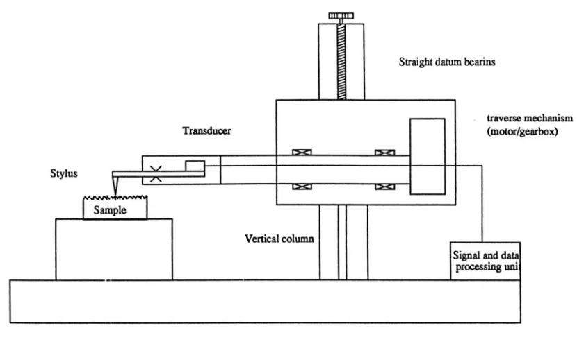
pro-filing in both the workshop and research laboratory. A typical stylus instrument
usually consists of five basic components, 1) a relative displacement transducer,
2) a datum surface, 3) a traverse mechanism, 4) a stylus probe, and 5) a signal
and data processing unit. Fig. 1.2 shows a schematic diagram of the instrument.
Although the structure details of the instruments may vary considerably, their
general arrangements nearly all conform to it [8]. In the system shown in Fig. 1.2,
a beam, pivoted on a knife edges, carries the stylus at one end and a transducer at the other. When measuring, the stylus is contacted and drawn by the traverse mechanism across the surface under examination. The irregularities of surface
cause the stylus to move vertically, and the motion is sensed by a transducer that monitors the deflection of the beam. The displacement of the stylus relative to a
datum surface is then used as a quantitative measurement of the surface profile.
A commonly used stylus transducer is an inductive gauge, LVDT or LVDI,
in which a ferromagnetic slug is usually fixed on the beam and located between
coils. When the stylus moves and the beam deflects, it causes a change in the
mutual inductance in the coils modulating a high frequency carrier signal in
pro-portion to the displacement of the stylus. In addition, some other displacement
transducers such as optical interferometers and capacitors are also found in mod-ern instruments [9]. All these transducers are of high sensitivity and capable of
1.2 Instrumentation [or surface metrology
Transducer
...
Stylus I
11-1
1
~"
I
SampleVertical column
on llJ
=
"'""""'
4
Straight datum bearins
- traverse mechanism
earbox)
(motor/g
[image:22.523.54.469.105.353.2]
-I
Signal ~ da~ processlIlg unJFigure 1.2: Schematic diagram of typical stylus instrument
system uses thc: measuring surface itself as a reference to generate the datum
-the locus of the skid center, as shown in Fig 1.3 (a). It functions like a
mechani-cal filter, corresponding to information of small scale surface features, but losing
the form and waviness information. Because only local surface "roughness" is
of interest, in it majority of engineering applications this type of datum can be
widely used. The independent datum is often defined by an optically flat surface
on which the stylus traverse arm is rested, as shown in Fig 1.3 (b). This datum
system has its mechanical loop open and, therefore, is susceptible to external
vi-bration. Almost all styli are diamond, with the most common shapes being either
conical with a 2 J-Lm radius tip or 90° pyramids with the tip truncated to a 2 J-Lm
square or somHimes 0.1 x 2.5J.lm like chisel. The finite dimensions of the stylus
ine'vitably produce a high frequency filter characteristic, exaggerating the radius
of peak's curvature and reducing the width of troughs
[11] [12].
The interactionbetween stylus and surface is predominantly a mechanical contact. This makes the measurement less sensitive to surface contaminations and what is measured is
1.2 Instrumentation for surface metrology
Locus of skid center
_---~~\-~LE:;;:-~~:::;~~~_-~
Skid
(a) Slciddatum
o
Optical flat datum surface
(b) independent datum
Figure 1.3: Schematic diagram of stylus datum systems
5
deformation and micro-scratches on some engineering surfaces, preventing its use
on soft specimens. The relative low dynamic response is another drawback of
the instrument, which limits the speed of measurement and makes "in process"
measurement difficult.
1.2.2 Optical methods
Although the stylus techniques are of great versatility, their drawbacks such as
contact deformation and slow response limit their use in many applications. There
are many othel conventional techniques for surface measurement, such as optical,
capacitive and pneumatic methods. Among them, optical methods are considered
to be the most obvious complement to the tactile instruments [13]. The optical
methods can be generally divided into two categories: focused and area methods.
Focused methods
In focused met hods, a small spot of light beam scans over a surface under
mea-surement. The changes of reflected beam produce the information on the surface
texture. There are a large number of focused instruments that can be classified
1.2 Instrumentation for surface metrology 6
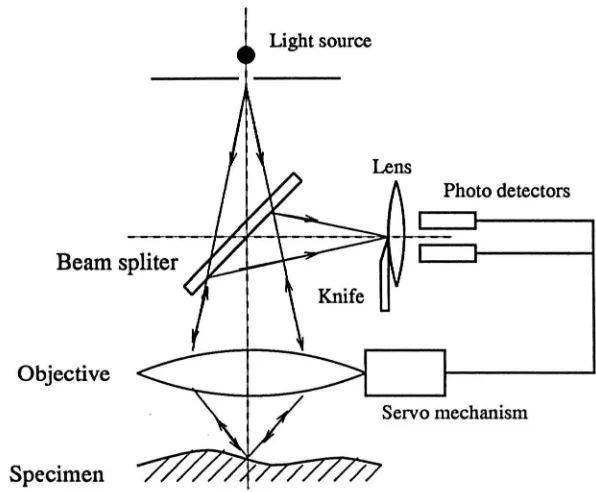
of the optical change does not have to be fully understood [14][15][16][17]. The
feedback signals from photo diode sensors are used to control a servo mechanism
which moves ohjective to follow the surface profile by keeping the light spot in
focus. Fig. lA illustrates a simple optical arrangement of the follower deviced
by Dupuy based on the principle of the Foucault knife-edge test
[i4].
Light source
Objective
Specimen
Figure 1.4: Optical arrangement of Foucault knife-edge follower
The defect-of-focus method is a non-follower focused technique [18], which
uses a comparison of the differences of the intensities obtained by two photo
detectors to sense the relative surface height. Most of these focused methods
have a vertical resolution similar to that of stylus technique and the output of
these instruments is analogous to the profile traces recorded by stylus instrument.
Because of its nature of non-contad and high speed, the instruments based on
this or similar principles may become a serious rival to stylus instruments in the
market-place as the level of sophistication and accuracy of these devices improves
[19]. The fundamental problem associate with the optical stylus to simulate the
[image:24.522.112.410.227.473.2]1.2 Instrumentation for surface metrology 7
limited by the Rayleigh criterion for resolution [1]:
(1.1 )
where Sd is the diffraction-limited spot size, J.L is the refractive in,dex between the
medium and the object and sin a is the effective numerical aperture of the lens.
The depth of focus D I is defined as the change in focal position for an increase in beam diameter (if, of
V2
is given):D = 1.22'\
I J.L sin a tan a (1.2)
However, recent development of scanning near-field optical microscopy breaks
. the barriers [20] and may make optical technique more competitive in surface metrology (more on these later).
Area methods
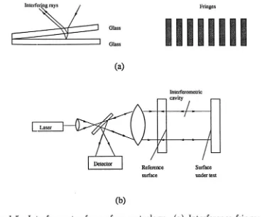
Interference microscopy is a popular technique in area methods. If two slightly
inclined glass plates are illuminated by. a coherent monochromatic light source, a
series of inference fringes will be visible, as shown in Fig. 1.5 (a). The distance
between neighbouring fringes is ,\/2. If these two glass plates are replaced by
a reference plane and a specimen, a. contour pattern of the surface texture will
be generated by the interference between light beams from these two surfaces.
There are many types of interferometers such as Newton, Twyman-Green, Fizeau,
Michelson and Mach-Zehnder interferometers [21]. Among them, Fizeau
interfer-ometer is the most commonly used, the optical arrangement of which is shown in
Fig. 1.5 (b). The interferograms can be not only analyzed directly by visual
ob-servation, but "Iso digitized using a CCD camera and analyzed by computer with
which higher resolution and morf> detailed information can be obtained [22) [23].
In the phase measuring interferometer (PMI), the phase of the cavity is changed
1.2 Instrumentation for surface metrology 8 many PMI algorithms to interpolate the phase changes in interferogram. Vertical and lateral resolutions of 0.5 nm and 1.25 11m is claimed [23].
Er=::;;Inte~":s~'
g==ray~, ~~/==::J=:,
Glass- Glass
(a)
surface
(b)
Fringes
11111111
Interferometric
cavity [image:26.523.81.454.163.468.2]under
test
Figure 1.5: Interferometer for surface metrology, (a) Interference fringes, (b) Fizeau interferometer
Miscellaneous
All of the optical methods mentioned above measure surface topography directly,
while other optical techniques use the reflection of light to quantify surface
rough-ness in parametric terms. Many of these methods can provide surface roughrough-ness
data in very short time, so they have considerable potential for "in process" application. Scattering measurement is one of these methods, which uses the
1.2 Instrumentation for surface metrology 9
properties [25]. The optical scattering instruments give excellent results for the
features down to optical wavelengths. To extend the information to
subnanome-ter features, wavelengths of similar order are needed. Recent advances in X-ray
instrumentation have made the measurement of surface roughness and
topogra-phy at nanometer level available by using specular or diffuse X-ray scattering
technique [7]. Fig. 1.6 shows a schematic arrangement of X-ray reflectometry. A
beam conditioner is used to collimate the X-rays providing a incident beam with
very small divffgence, and a detector captures the reflected beam from which
the surface roughness information is extracted by a computer using an efficient
algorithm. The surfaces only show strong specular reflectivity near the critical
angle for total external reflection, so that the specimens have to be flat enough
to allow the beam to be incident at the grazing angle. The method averages
the reflected X .. rays over an are(l of a few square millimeters. The quantitative
information on roughness between 0.05 and 5 nm, on correlation lengths from
sub-nanometer to tens of micrometers have been claimed [27].
Detector X-ray source
r----,
\~
~
SplitBeam conditioner ~
Specimen
Figure 1.6: Schematic arrangement of X-ray reflectometry
1.2.3 Modern scanning microscopies
As the result of rapid development of precision engineering, the requirements
on measurement of surface topography have become ever more increased and
strict. Many conventional methods based upon stylus and optical techniques
1.2 Instrument.'ttion for surface metrology 10
However, their lateral resolution is poor, usually of order about one micrometer,
which is inadequate for the characterization of current advanced materials and
for the application in nano-fabrication technology. Almost all of the modern
microscopies such as electron microscopy and scanning probe microscopy have a
significant improvement in lateral resolution. Therefore very fine details of surface
feature can be distinguished, even sometimes atomic images can be obtained.
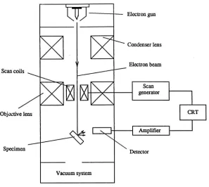
Electron microscopy uses electron beams to form magnified images of surface topography. The very short wavelength of the electron beam makes it much more
superior to optical methods in respect of lateral resolution and the depth of
res-olution. A scanning electron microscope (SEM) can resolve to approximately 3
nm and a transmission electron microscope (TEM) to about 0.2 nm [28]. The
SEM has become a very popular tool for observation and investigation of surface
feature in engineering due to its versatility, and the use of TEM is not as
pop-ular as SEM because of the difficulty in preparing specimens thin enough to be measured. A basic diagram of an SEM is shown in Fig. 1.7. Electrons from a filament are accelerated by a high voltage and condensed by the condenser lens
and then focused by the objective lens. Scanning coils located within the
objec-tive lens cause the electron spot scanning over the specimen. A detector captures
usually the sewndary electrons emitted from the surface and transfer them into
signal for displ.!y on a CRT screen. The principal drawback of the method is that
the interpretation of the images is not necessarily straight forward and they do not readily yield quantitative data about the height of surface feature. Although
many attempts have been made tb derive such data from the process [29] [30] [31], the result,; are, so far, still not reliable enough for practical application.
The introduction of scanning tunneling microscope (STM) in 1982 by G.
Bin-nig and H. Roher has had a great impact on surface science. Meanwhile, it has
stimulated an entir~ family of scanning probe microscopes (SPM) which mea-sure a range of physical and chemical properties of a surface on the nanometer or
1.2 Instrumentation for surface metrology 11
- - - f - - Electron gun
Condenser lens
Electron beam Scan coils
Amplifier
Specimen
Detector
[image:29.522.119.416.110.376.2]Vacuum system
Figure 1. 7: Schematic diagram of an SEM
criterion which assumes that the ultimate resolution of optical systems will be limited by the wavelength of the radiation used to form the image is surpassed.
The resolution of the SPMs has approached to the physical limit of
instrumenta-tion. Their applications have not been limited to surface measurement, but also
expanded to surface manipulation for subnanometer machining, single atom ma-nipulation as well as a variety of chemical and biological processes. More details
about SPM are reviewed in chapter 2. For surface metrology, scanning tunneling
and atomic force microscopes are most commonly used. The atomic force
mi-croscope (AFM), or scanning force microscope (SFM), is more versatile for the
measurement of surface topography because it can measure not only
conduct-ing but also non-conducting specimens. The SFM is similar to stylus techniques
in principle, therefore the measurement is that of the mechanical surface. The
research work of this thesis is aimed to improve SFM instrumentation with
1.2 Instrumentation for surface metrology 12
Bibliography
[1] D.J. Whitehouse, 1994, Handbook of surface metrology, lOP publishing Ltd.
[2] I. Sherington and E.H. Smith, 1986, The significance of surface metrology in engineering, Precision Engineering, 1 79 - 87
[3] T.R. Thomas, 1975, Recent advances in the measurement and analysis of
surface micro geometry, Wear, 33 205 - 233
[4] D.J. Whitehouse, 1985, Assessment of surface finish profiles produced by
multi-process manufacture, Proc. lnstn. Mech. Engrs. 199
B4,
263 - 270[5] N. Taniguchi, 1974, On the basic concept of nanotechnology, Proceedings of
the ICPE, Tokyo
[6] N. Taniguchi, 1994, The state of the art of nanotechnology for processing of
ultraprecision and ultrafine products, Precision Engineering, 16 (1), 5 -
24
[7] D.J. Whitehouse, 1978, Surface metrology instrumentation, J. Phys., E 20
1145 - 1155
[8] D.G. Chetwynd and S.T. Smith, 1991, High precision surface profilometry:
from stylus to STM, From instrumentation to nanotechnology, edited by J. W. Gardner and H. T. Hingle, Gordon and Breach Science Publishers, 273 - 300
",
[9] J.D. Garratt, 1979, Survey of displacement transducers below 50 mm, J.
Phys., E 12, 563 - 573
BIBLIOGRAPHY 14
[10] I. Sherrington and E.H. Smith, 1988, Modern measurement techniques in surface metrology: part I; stylus instruments, electron microscopy and
non-optical comparators, Wear, 125 271 - 288
[11] D.J. Whitehouse, Theoretical analysis of stylus integration, Ann. CIRP, 23,
181 - 182
[12] V. Radhakrishnan, 1970, Effect of stylus radius on the roughness values
measured with tracing stylus instruments, Wear, 16, 325 - 335
[13] R.D. Young, T.V. Vorburger and E.C. Teague, 1980, In process and on line
measurement of surface finish, Ann. CIRP, 29 435 - 439
[14] O. Dupuy, 1967-1968, High precision optical profilometer for the study of
micro-geometrical surface defects, Proc. Inst. Mech. Eng., London, 182 {3k}, 255 - 259
[15] Fang-Sheng Jing, A.W. Hartman and R.J. Hocken, Noncontacting optical
probe, Rev. Sci. Instrum., 58 {5}, 864 - 868
[16] F.T. Arecchi, D. Bertani and S. Ciliberto, A fast versatile optical
profilome-ter, Opt. Comm., 31 {30}, 263 - 266
[17] Y. Fairman, E. Lenz and J. Shamir, 1982, Optical profilometer: a new
method for high sensitivity and wide dynamic range, Appl. Opt., 21 {7},
3200 - 3208
[18] J. Mignot and C. Gorecki, 1983, Measurement of surface roughness
compar-ison betwe~n a defected of focus optical technique and the classical stylus technique, Wear, 81, 39 - 49
[19] I. Sherrington and E.H. Smith, 1988, Modern measurement techniques in
BIBLIOGRAPHY 15
[20] D.W. Pohl, W. Denk and M. Lanz, 1984, Optical stethoscopy: image
record-ing with resolution ),,/20, Appl. Phys. Lett., 44, 651 - 653
[21] L.A. Selberg, 1994, Interferometric metrology: an introduction, Tutorial of
ASPE 9th Annual Meeting, Cincinnati, October
[22] S. So and K. Wong, A hybrid optical-digital image processing method for
surface inspection, IBM J. Res: Dev., 27
(4)
276 - 385[23] J.C. WyaHt, C.L. Koliopoulos, B. Bhushan and D. Basila, 1986, Development of a three dimensional noncontact digital optical profiler, J. Tribol., 108, 1 - 8
[24] K.J. Stout, 1984, Optical assessment of surface roughness, Precis. Eng., 6
(1),
35 - 3.9[25] J.K. Rakels, 1991, Optical diffraction for surface roughness measurement, From instr'umentation to nanotechnoloy, edited by J. W. Gardner and H. T. Hingle, Gordon and Breach Science Publishers, 227 - 254
[26] D.K. Bowen and B.K. Tanner, 1993, Characterization of engineering surfaces
by grazing incidence X-ray reflectivity, Nanotechnology, 4, 175 - 182
[27] D.K. Bowen and M. Wormington, 1994, Measurement of surface roughnesses
and topography at nanometer levels by diffuse X-ray scattering, Ann. of the
CIRP, 43, 497 - 500
[28] S.L. Fleglt!r, J.W. Heckman, Jr. and K.L. Klomparens, 1993, Scanning
and transmission electron microscopy - an introduction, W.H. Freeman and
Company, New York
[29] M. Rasigm, G. Rasigni, J.P. Palmori and A. Llebaria, 1981, Validity of
surface roughness study using microdensitometer analysis of electron
BIBLIOGRAPHY 16
[30] D.W. Butler, 1973, A stereo electron microscope technique for
microtopo-graphic measurements, Micron, 4, 410 - 424
[31] Y. Matsuno, H. Yamada and A. Kobayashi, 1975, The microtopography of
the grinding wheel surface with SEM, Ann. CIRP, 24 (1),.237 - 242
[32] H.K. Wickramasingle, 1992, Scanned probes old and new, Scanned probe
microscopy, edited by H.K. Wickramasingle, American Institute of Physics,
Chapter 2
Development of scanning probe
•
mIcroscopes
Since an atomi::. image was first achieved by Binnig and his coworkers, 1982 [1] [2],
using the scanning tunneling microscope, subsequent developments have resulted
in the emergence of an entire family of SPMs from scanning tunneling and atomic
force microscopes to th~se based on sensing techniques of capacitance, magnetic,
near-field optic, thermal, ion-conductance and many other near-field physical
and chemical properties. From the instrumentation point of view, all these have
similar principles of operation with any particular design consisting of
1) A probe transducer system.
2) A three dimension positioning and scanning mechanism.
3) A control system.
4) Data processing and imaging software.
2.1
Scanning probe microscopy
2.1.1 Scanning tunneling microscopy
The scanning t.unneling microscope (STM) is an example of a super resolution microscope capable of atomic imaginl!;.. In the STM, the probe consists of a
2.1 Scanning probe microscopy 18
fine metal tip which is positioned in close proximity to a conducting surface
with a voltage applied between them. The separation between tip and sample
is sufficiently small that electrons can tunnel across and therefore generate a
current. For all idealized one-dimensional planar tunneling model, when the gap
is small and the voltage low, the current-gap distance relation can be simplified to [3]
-1
I ex (V/d)exp( -A~2 d) (2.1)
0 -1
where A
=
1.025(eV)-1/2A , V is the bias voltage between the sample and thetip, d is the gap distance and ~ is average of the barrier height between the two electrodes. It indicates that the tunneling current varies exponentially as
o
gap distance changes. Actually, 1 A change in the gap distance can produce an
, order of magnitude change of the tunneling current with «I> '" 4e V. By this,
displacement of 10-4
A
can be measured. This phenomenon was first introducedinto metrological application as a field emission ultramicrometer by Young, 1966 [4], and possible applications of contact free measurement of surface profiles or
surface contours were proposed. After that, the first surface profile measuring
instrument based on field emission was invented by Young et al. 1972 [5], called
"Topografiner". In this instrument, a tungsten tip (emitter) is held on an x-y-z
piezoelectric trc.nslation stage. The specimen is brought to the probe close enough
so that it is within the range of z piezo translator using a differential micrometer.
The current in the gap is fed back to a servo controller to maintain a constant field emission current and hence a fixed gap distance. As the tip is scanned
lat-erally across the specimen, the changes of z piezo driver voltage are interpreted into the variations of surface height, Although the subnanometer resolution was
not achieved by this instrument, tunnelling was demonstrated and STM
instru-mentation proposed. Ten years later, a working scanning tunneling microscope
system was built by Binnig and Rohrer, 1982, [1] [2]. Their device had good vi-bration isolation and stable feedback servo controller and was maintained under
sepa-2.1 Scanning probe microscopy 19
ration of a few Angstroms, so that a tunneling current is obtained. At this time,
atomically resolved images were obtained such as topographic maps of Calr Sn4
and Au (110) surface and an image of the 7 X 7 Reconstruction on Si(111) [6] .
Stimulated by these results, there was a boom in research to further understand
tunneling mechanisms, improve instrumentation and explore new applications of
this technology. Therefore, their work was generally considered as a pivot for the
development of whole range of scanning microscopes based on local probes.
2.1.2 Scanning force microscopy
Although the STM conducts atomical imaging successfully, it operates only with conducting surfaces. This prevents its normal application on an insulator or in
. a working environment in the presence of surface contamination. The invention
of the atomic force microscope (AFM), also by Binnig and his coworkers 1986 [7]
solved this problem. The AFM probe measures minute changes in force between
the tip and the surface as a means of proximity detection. Therefore, it can image nonconducting as well as conducting sample surfaces.
In the AFM, a sharp tip is attached to the end of a small cantilever beam
which bends dt'.e to van der Waals interatomic (or intermolecular) forces as the
tip is brought into near proximity to the surface. The deflections of the beam are
monitored with a sensitive detector. The signals from the detector are used to
servo a vertical piezoelectric translator on which the force probe (or specimen) is
mounted to maintain a constant force acting between the tip and the specimen
as the tip scans across the surface, as shown in Fig. 2.1. The short range nature
of the interatomic, or intermolecular, forces makes it possible for the AFM to
get high resolution in both the vertical and lateral directions. Atomic resolution images have also been achieved lu,ing this technique [8].
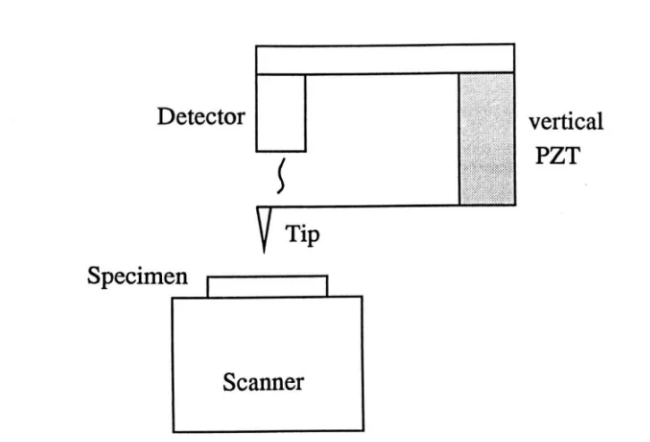
2.1 Scanning probe microscopy
Detector
Tip
Specimen '..---"1
Scanner
vertical
PZT
[image:38.525.69.432.90.337.2]20
Figure 2.1: Schametic diagram of the configuration of atomic scanning microscope
of
2
to3
A
[9],
below which interatomic forces are always repulsive, and abovewhich they appear attractive within a certain range. According to Lennard-Jones
potential, the main forces involved in the interatomic interactions can be classified
as
A) electrostatic or Coulomb interactions between charges or charge
distribu-tion, such as m:mopoles, dipoles, quadrupoles, and their combinations.
B) polarization forces, where a distribution of charges in one molecule create
a dipole moment in an adjacent molecule.
C) quantum mechanical forces, which give rise to covalent bonding and to
repulsive exchange interactions.
The experimentally derived Lennard-Jones molecular interaction energy,
com-bining the attr2.ctive van der Waals and repulsive atomic potentials, provides an
easily understood view of general properties of these interaction forces:
2.1 Scanning probe microscopy 21
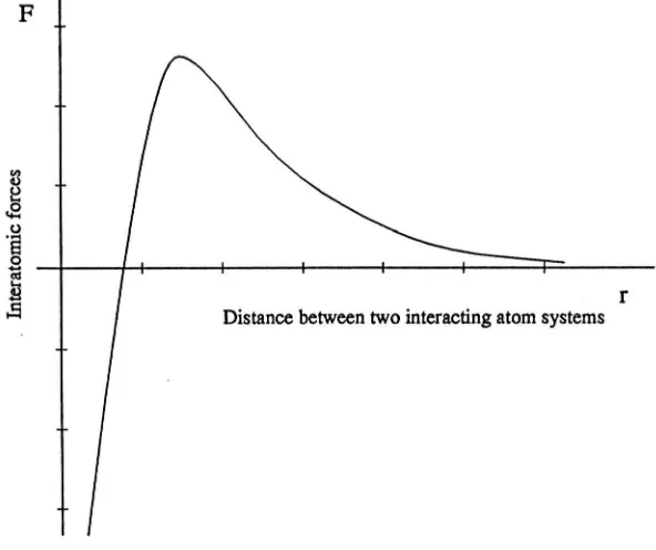
The forces are obtained by differentiating equation 2.2, yielding
(2.3)
where, r is distance between two interacting atom systems, Wo and (J are
exper-imentally derived constants. This force and distance relationship is plotted in
Fig. 2.2 without a scaling for demonstration purpose,
F
~
.E u
·
s
~
~----~----~----~----~--~====~=----r--.s
Distance between two interacting atom systemsFigure 2.2: The plot of interatomic force
The real ca~es for these interatomic forces are far more complicated and are
not encountered in AFM which 'see' only many body interactions. Discussions
on that are beyond the scope of our interests in the thesis. More details can be
found in references [9][10].
Corresponding to the characteristics of the interatomic forces, there are two
distinct operation modes of the AFMs, attractive (noncontact) mode or repulsive
(contact) mode. In the first, the probe is approached to the surface until a
[image:39.522.111.407.262.510.2]2.1 Scanning probe microscopy 22
while the surface is moved relatively to it, the probe will move following the
contour. The second mode is achieved by reducing the probe to surface separation
until a repulsive force is encountered. This is directly analogous to conventional
stylus profilometry only the force is maintained at a constant value which may
be in the region of nanonewtons, which is three to six orders of magnitude lower
than the forces commonly used with the stylus. Because of the short range
nature, the AFMs working in repulsive mode are capable of achieving atomic
resolution. In contrast, attractive mode AFMs operate with relatively large tip-sample distan(cs and it is therefore difficult to reach the same resolution. Its
probe usually has interacting forces which are much smaller than that encountered
by repulsive mode AFM, so that resonance enhancement techniques are required. In this case, the cantilever beam is vibrated and the changes of the vibration
caused by small variation of the attractive forces or force deviatives are monitored
and interpreted into profile information. Sarid gave a good summary on the enhancement tf..chniques in his book [9].
Attractive mode scanning force microscopes have been used to conduct a
number of novel measurements ranging from non-contact profiling of surfaces to magnetic [12] and electrostatic imaging [13].
In magnetic force microscopy (MFM), the tip is replaced by a magnetic one
typically iron or nickel and a magnetic interacting force between tip and sample is
detected. The topography measured over a fiat magnetic surface can be directly related to its magnetic features.
In the electrostatic force microscopy (EFM), an AC voltage is applied between
tip and sample and the induced force is sensed. The force is proportional to the square of the applied voltage V2 times the rate of change of tip-sample capacitance with spacing, {)C /
aT.
By keeping the spacing constant the surface topograph can thus be measured.2.1 Scanning probe microscopy 23
2.1.3 Scanning near-field optical microscopy
In a long history of the development of optical microscopy, it was conventionally
believed that the ultimate spatial resolution that can be achieved in any optical system is roughly one half the wavelength of the radiation used to form the
images - the so called Rayleigh criterion (from equation 1.1). This limit was not
surpassed until the invention of scanning near-field optical microscopy (SNOM).
In this technique, an optical probe with a tiny aperture at the end of the tip
is illuminated from the base side and scanned along the sample in very close
proximity, typically less than 5nm. As a result, a scanning optical micrograph of
the surface can be obtained, in which the lateral resolution is determined by the tip probe diameter and not by the wavelength of the radiation. Since the optical
. probe tip can be fabricated to the order of 10nm in diameter, SNOM offers
the possibility of spatial resolution far exceeding the Raleigh limit. The papers
written by Durig et al.
[14]
and Isaacson et al.[15]
give a good introduction and review of this technique.2.1.4 Scanning capacitance microscopy
Capacitance has been used as the basis of a local probe resulting in the
devel-opment of scanning capacitance microscopy (SCM), which provides a means for
surface characterization through the measurement of local capacitance between
tip and sample. A conductive tip is usually used as one of the electrodes and
the other electrode, sample, can be either conductive or nonconductive. The
capacitance or local charge storage between the proximal tip and sample forms
the interaction. Therefore, both conductors and insulators can be profiled with
SCM. If feed back control is used to scan the tip at constant gap across a sample, noncontact surface profiling can be realized. Explored by Matey
[16],
thescan-.
'\2.1 Scanning probe microscopy 24
a near-field capacitance microscope built by Williams et al. [18], a capacitance
image with resolution less than 25nm has been achieved. Another unique
capa-bility of the technique is that it can measure buried conducting layers. This is
potentially useful for semiconductor applications.
The capacitance method suffers from the problem that it measures variation in
dielectric as well as topography. With current microscope designs the sensitivity is not as high as other near-field probe techniques.
2.1.5 Scanning thermal microscopy
Thermal imaging is another novel application of SPM. Scanning thermal
mi-croscopy (SThM) is to measure thermal interactions between tip and sample using
SPM technique. The first scanning thermal microscope was built by Williams and
Wickramsinghe (1986) [19], which aimed to overcome the inability of the STM to image non-conductive surfaces since the AFM was not well developed at that time. The thermal probe consists of a thermo-couple junction built at the end of
a tungsten tip (50nm in diameter). The probe is heated and brought within near proximity of surface. The thermo-couple junction is used to measure the temper-ature change due to the conduction of heat between the tip and sample via air.
This provides the feedba.ck signal to maintain constant tip-sample spacing during
lateral scan. Because of the large difference in thermal conductivities between air
and solids, the measurements tends to be independent of the material properties.
However, temperature changes on the scan surface may appear as features on
surface image thus making it difficult to separate temperature from
topographi-cal variations, and the surface temperature can not be imaged separately. These
limit the applic.ation of the technique.
Weaver et al. [20] modified a STM to make a tunneling thermometer in
or-der to measure optical absorption of thin metal film, achieving a 1 nm spatial
resolution. More recently, atomic force microscopes have been used for thermal
2.2 SFM transduction methods 25
this method, simultaneous thermal and topographical measurement becomes pos-sible and thermal image and topographical image can be obtained separately. So
called "passivell
and "active" thermal measurement modes can be implemented. In the "passive" mode, the thermo-couple is only used to measure the surface
temperature, so that temperature image is obtained. In the "active" mode, the
thermo-couple is heated. The heat flow between the probe and sample will be
influenced by the thermal conductivity of the sample and the temperature
dif-ference. In this case, it is possible to image the thermal properties of the sample surface or subsurface.
2.2
SFM transduction methods
, A force detecti on system is essential for the realization of the scanning force
microscopies mentioned above. Common to the force detection system is the use
of a delicate transducer that measures the minute force-induced deflections of a
flexible cantilever supporting the force sensing tip. The output of this is used to maintain the constant force feedback. Many possible sensing techniques have been tried for t.he deflection monitoring, of which some of the more successful are outlined below.
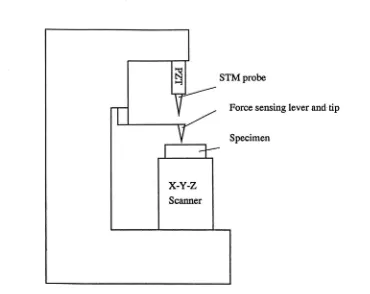
2.2.1 Tunneling detection system
In the first atomic force microscope invented by Binnig et al. [7], electron
tun-neling was used for its force detection system. The working principle of the
tunneling detection system is shown schematically in Fig. 2.3. In this system,
the minute deHections of the force sensing lever is monitored by a STM probe which measures the tunneling current from the back of the cantilever. The
sig-nals from the STM probe are fed to the servo controller for the z translator of
2.2 SFM transduction metbods
X-Y-Z
Scanner
STMprobe
Force sensing lever and· tip
Specimen
Figure 2.3: Schematic diagram of tunneling detection system
26
small as 10-4
.~i,
corresponding to a force of 10-16 N if a cantilever of O.OlN/min stiffness is used, and by vibrating the lever, the sensitivity to force can be
further increased [7]. Atomic resolution has been achieved using the AFM with
tunneling detection system by Binnig and Rohrer 1987 [25], Marti et al 1987
[26] and Kirk et al. 1988 [27]. However, some problems were encountered in its
applications. Local topography of the cantilever surface and contaminants on
tunneling interfaces can be detrimental to the stability of the tunneling current.
The proximity of the tunneling tip and the cantilever will also introduce the
ef-fect of interaction atomic forces, resulting in further interpretation problems of
measurement results. These problems make it unreliable for use as the tip force
detector in air or even in UHV. Although it is an extremely sensitive transducer
for high resolu~ion displacement, it has become less favoured for force detection
[image:44.522.69.439.85.379.2]2.2 SFM transduction methods 27
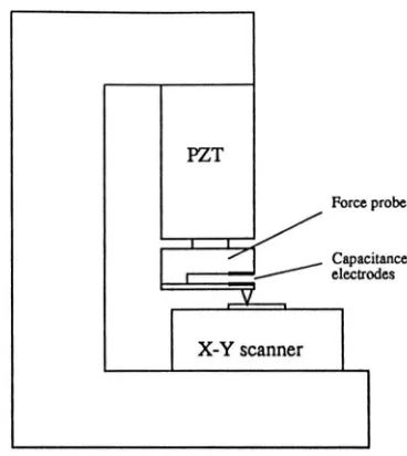
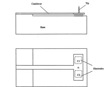
2.2.2 Capacitance detection system
Capacitance displacement detection is an alternative method for monitoring the
minute deflections of the force sensing cantilever. Fig. 2.4 shows a diagram of
capacitance based force probe system. A stationary electrode is located very close
to the back face of the force sensing cantilever to form a capacitance sensor. The gap between the electrodes is usually in the region of a few micrometers. The
capacitance changes caused by force-induced cantilever displacement can be
de-tected using a transformer bridge. Again, the signal from the capacitance gauge is used for servo control of z PZT to maintain constant contact force during
scan-ning. The capacitance detection measures the average effect of the two electrode surfaces, so that it is much less susceptible to the local conditions of detecting
area than STM detection. Therefore it is a more stable and reliable detection
method and can be made compact in structure. In previous work by T.
Godden-henrich, et al. using capacitance detection in their magnetic force microscope, a minimum force 10-10 N was reported [28]. The SFM built by G. Neubauer, et al., [29] using bidirection~ capacitance sensing technique for simultaneous
mea-o surements of normal and lateral forces, achieved a vertical resolution of 10
A
andnoise level of 0.03
A
RMS. Design details of the capacitance based force probewill be discussed in Chapter 3.
Another novel application of the capacitance sensor is its additional use for
electrostatic force balance. Generally, the force sensing modes of AFM can be
divided into two classes simply known as "de" and "ae" modes. In the de
mi-croscope, the interaction force between tip and sample is directly sensed through
the static deflection of a weak cantilever when the tip is in the proximity of the sample. To achieve high sensitivity requires a low spring constant. It, however,
makes operation in the attractive mode difficult. When the probe-sample force
gradient, 8F/8z, where z is the surface separation, exceeds the spring constant of
the cantilever, instability of cantilever-tip-sample potential will occur, i.e. the tip
detect-2.2 SFM transduction metbods
I
PZT
Porce probe
, / ~ Capaci
electr tance
odes
]J..
[image:46.523.164.348.107.313.2]x-v scanner
I
Figure 2.4: Schematic diagram of capacitance detection system
28
ing the force gradient through variations in either the amplitude or the frequency
of a vibrating ~;tiffer cantilever. In this way, however, the force is not directly
available. By llsing the cantilever having large spring constant in de mode, the
instability can be reduced, but the force sensitivity will decrease as well. A
solu-tion for the problem is electrostatic force balanced force probe explored by Joyce
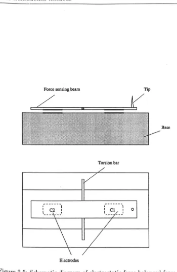
and Houston (1991) [30] and Miller et al. (1991) [31]. Fig. 2.5 shows a schematic
diagram of the probe. A force sensing beam, with a tip mounted on the end of it,
IS centrally supported by a torsion bar which is, in turn, rigidly fixed on a solid
base. A small gap exists between the beam and the base. Two electrodes (Cl
and C2) on the opposite surfaces of them forms a differential capacitance sensor
monitoring beam's position using an rf phase shift technique.
A positive voltage is applied to each of t.he two electrodes inducing an
elec-trostatic force
J"c
on the beam, which is given by(2.4)
2.2 SFM transduction rnetllOds 29
Force sensing beam
/
Base
Torsion bar
L
v/
---...
---I I I I
I
C2 I I Cl I 0
1 ---\--~ I
1_
-:l--}
\
/
\
/
\
/
Electrodes
[image:47.528.68.418.66.603.2]