ISSN Online: 2153-1293 ISSN Print: 2153-1285
DOI: 10.4236/cs.2017.811019 Nov. 29, 2017 261 Circuits and Systems
Analysis of Electronic Circuits with the Signal
Flow Graph Method
Feim Ridvan Rasim, Sebastian M. Sattler
Friedrich-Alexander-University Erlangen-Nuremberg, Chair of Reliable Circuits and Systems Paul-Gordan, Erlangen, Germany
Abstract
In this work a method called “signal flow graph (SFG)” is presented. A sig-nal-flow graph describes a system by its signal flow by directed and weighted graph; the signals are applied to nodes and functions on edges. The edges of the signal flow graph are small processing units, through which the incoming signals are processed in a certain form. In this case, the result is sent to the outgoing node. The SFG allows a good visual inspection into complex feed-back problems. Furthermore such a presentation allows for a clear and unam-biguous description of a generating system, for example, a netview. A Signal Flow Graph (SFG) allows a fast and practical network analysis based on a clear data presentation in graphic format of the mathematical linear equations of the circuit. During creation of a SFG the Direct Current-Case (DC-Case) was observed since the correct current and voltage directions was drawn from zero frequency. In addition, the mathematical axioms, which are based on field algebra, are declared. In this work we show you in addition: How we check our SFG whether it is a consistent system or not. A signal flow graph can be verified by generating the identity of the signal flow graph itself, illu-strated by the inverse signal flow graph (SFG−1). Two signal flow graphs are always generated from one circuit, so that the signal flow diagram already presented in previous sections corresponds to only half of the solution. The other half of the solution is the so-called identity, which represents the (SFG−1). If these two graphs are superposed with one another, so called 1-edges are created at the node points. In Boolean algebra, these 1-edges are given the value 1, whereas this value can be identified with a zero in the field algebra.
Keywords
Analog, Feedback, Network Theory, Symbolic Analysis, Signal Flow Graph, Transfer Function
How to cite this paper: Rasim, F.R. and Sattler, S.M. (2017) Analysis of Electronic Circuits with the Signal Flow Graph Me-thod. Circuits and Systems, 8, 261-274. https://doi.org/10.4236/cs.2017.811019
Received: October 16, 2017 Accepted: November 26, 2017 Published: November 29, 2017
Copyright © 2017 by authors and Scientific Research Publishing Inc. This work is licensed under the Creative Commons Attribution International License (CC BY 4.0).
DOI: 10.4236/cs.2017.811019 262 Circuits and Systems
1. Introduction
There are various methods in the circuit technology to ca1culate transfer func-tions of electrical circuits such as Kirchhoff’s laws, two-port network theory, nodal analysis method [1] and time constant method [2]. These methods are generally time-consuming and computationally intensive. Moreover, it is always useful to develop a common graphical model, with using this model to make a connection between the state variables (parameters) and the transfer function as well as to obtain a better understanding of the complex functionality of a net-work. Using mesh rules, node rules and Ohm’s equations a signal flow graph can be build. Targeted minimization of subgraphs, allows the ca1culation of a trans-fer function easier. In this paper we repeat the mathematical methodology for the symbolic analysis of real electronic circuits on the basis of a given real cir-cuitry. It is based on graph theory, the so called SFG method. The signal flow graph (SFG) is a vividly method to present the internal structure of a system or the interaction of several systems. This presentation allows a better understand-ing of the function as well as the interrelations of one or more systems. Signal flow graphs are formally defined graphs [3]. Such a mapping enables a one-to-one (local-bijective) and understandable description of a generating sys-tem. It serves to increase clarity as well as contribute to an understanding of the circuit. The SFG allows a further comprehensible and simple visual considera-tion of the problem. It shows us all the funcconsidera-tions of every part in the circuit and the connections between them. It is also a good method to help us to define the states in the circuit. It helps us to understand the circuit deeply and systemati-cally. In addition, physical connections of the circuit become more recognizable. For the understanding of the circuit, the signal flow graph is a suitable method for the representation. To present the application we use a Common-X circuit as a use case. First, the Common-X circuit is split into its subcircuits and for each subcircuit their associated SFGs are established. Then by the superposition of the SFGs of the subcircuits the total SFG for the Common-X circuit results.
Organization of the paper: First, the theoretical foundations are briefly ex-plained in Chapter 2. They are regarded as basic knowledge in order to under-stand this work. Subsequently, the implementation is described in detail in Chapter 3 and visualized by sketches and signal flow graphs. In the end, the re-sults and the core outline of the work are summarized again and an outlook is given.
2. Theoretical Foundations
DOI: 10.4236/cs.2017.811019 263 Circuits and Systems arrow on the edge. The edges of the signal flow graphs are small processing units, through which the incoming signals are processed in a certain form. In this case, the result is sent to the outgoing node [3]. In network theory are often used ohmic resistors, capacitors and inductors. When considering these ele-ments, the direction of the directed and weighted signal flow graph can not be interchanged easily. Prior to changing the direction of the arrow direction, the function on the edge has to be inverted. The material equation is given as an example. The signal flow graph with the respective function on the edge is shown in Figure 1 [8].
Figure 1. SFG of an inductance.
2.1. Elements of a Signal Flow Graph
A signal flow graph exists next to edges and nodes of paths, loops, input node and output node. A node is a point or a circle, which reproduces a signal or a va-riable. In order to illustrate these individual elements, the Figure 2 is to be in-vestigated in more detail.
Figure 2. Example of a signal flow graph (SFG).
This signal flow graph has six nodes and seven edges. A node is a point or a circle that represents a signal or a variable. In the example, the variables x1, x2 etc. represent a node. There are different types of nodes. A dependent node has one or more leading incoming edges and any number of leading outgoing edges. Input node (x0), also known as source node, has only outgoing paths and represent independent variables. An output node (x5), also known as sink node, has only incoming paths and is in contrast to the input node a dependent variable. A path is a connected sequence of edges in one direction, the connection of x1 to x3 by edges b c, via node x2 represents a path. The path gain is the product of the functions on the edges along a path. In this example, the path gain is b c⋅ . A reverse path is a path that leads towards the
[image:3.595.293.456.410.510.2]DOI: 10.4236/cs.2017.811019 264 Circuits and Systems connection via the edges b c, and g build a feedback loop, the initial loop is
1
x in this case. A feedback loop is present when the start and end nodes are the same. When the edges b c, and g pass through, we reach the original node
1: 1 2 3 1
x x →x →x →x . Loops are equal oriented edges forming a closed path and will touch no node multiply. A self-referential loop is exactly present when a path flows from one node in the same node without crossing other nodes [9].
2.2. Modifications of Signal Flow Graph
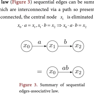
By associative law (Figure 3) sequential edges can be summarized. As soon as three nodes which are interconnected via a path so present, that there are the
0 1 2
x → →x x connected, the central node x1 is eliminated from the graph:
0 1, 1 2 0 2
x ⋅ =a x x b⋅ =x ⇒x ⋅ ⋅ =a b x
Figure 3. Summary of sequential edges-associative law.
Parallel running edges with the same input node x0 and output node x1 can be combined with the distributive law (Figure 4). The resulting graph is minimized to an edge. For example, two edges from node x0 flow into the node x1. Algebraically, the node x1 be expressed as:
(
)
0 0 0 1
x a⋅ + ⋅ = ⋅ +x b x a b =x
Figure 4. Summary of parallel edges-distributive law.
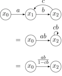
Dissolving a feedback loop (Figure 5): In order to eliminate the node x1, be first the functions multiplied on the edges along the forward path. Next, forming the product of the individual loop gains. This is the signal flow graph of two edges a b⋅ and c b⋅ , in which c b⋅ is a self-referential loop. Thus, the node
1
x is removed from the graph and the feedback has been summarized in a reflexive edge:
0 1, 1 2 0 2 2
x ⋅ =a x x b⋅ =x ⇒x ⋅ ⋅ + ⋅ ⋅ =a b x c b x
(
)
0 2 1 0 2
1
a b
x a b x c b x x
c b
⋅
⇒ ⋅ ⋅ = − ⋅ ⇒ =
[image:4.595.268.457.197.385.2]DOI: 10.4236/cs.2017.811019 265 Circuits and Systems
Figure 5. Dissolving a feed-back loop.
A reflexive edge (self-referential loop) can be eliminated, in which one by one divides the product of the functions on the edges toward the reflective edge minus the product of the functions on the reflexive edges. For more reflexive edges one can use the same procedure. In Figure 6, the reflexive edge resolved is shown with the corresponding weights [4] [6].
Figure 6. Dissolving a reflex-ive edge.
Example:
• Source node x0 • Sink node x4
• Target: Simplification of the SFG consists only of start and end nodes • Transfer Function G
[image:5.595.320.429.73.206.2] [image:5.595.202.487.329.728.2]DOI: 10.4236/cs.2017.811019 266 Circuits and Systems 2) Elimination of reflexive edges:
3) On the basis of the associative law, the nodes x2 and x3 are taken from the graph:
(
)(
)(
)
4
0 1 1 1
x a b d f
G
x c b c g
⋅ ⋅ ⋅
= =
− ⋅ − −
3. Analysis of Common X-Circuit
In this section, we will show you an example: How to set up the SFG, then by using SFG modification rules how to simplify the SFG to calculate the transfer function, and additionally how we check our SFG whether it is a consistent system or not?
DOI: 10.4236/cs.2017.811019 267 Circuits and Systems
[image:7.595.252.498.199.283.2]Figure 7. Small signal equivalent circuit of the CX-circuit.
Figure 8. Small signal equivalent circuit of the CX-circuit in sepa-rate form.
3.1. Analysis of First Subcircuit
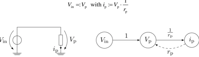
The first subcircuit is a simple voltage divider. Based on the above considerations (Figure 8) can now be derived for the first subcircuit of the signal flow graph (Figure 10). Before the signal flow graph is derived from the first subcircuit, the first subcircuit is to be simplified by a further step. If the resistor RY is taken out of the circuit, then a circuit with an ideal voltage source and a resistor is rp obtained, Figure 9. In the ideal case, the total voltage Vin drops across the resistance rp. The voltage source supplies the current ip as a function of the resistance rp. A voltage source should never be confused with a power source. The voltage source provides a current dependent on the load. On the other hand, the current source provides a constant current independent of the load. The mesh rules and the material equation yield the equations:
in p p p
p
1
: with :
V V i V
r
= = ⋅
Figure 9. First subcircuit (left) of the CX-circuit is simplified by RY and SFG (right) of the circuit.
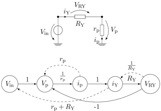
[image:7.595.213.536.523.616.2]DOI: 10.4236/cs.2017.811019 268 Circuits and Systems signal flow graph for the first sub circuit can now be derived much more easily. It is desirable that the total voltage Vin of the voltage source drops across the resistor rp. In reality, however, a small part of the voltage at the much smaller resistance RY drops. The desired voltage at the resistor rp can thus be ad-justed with the resistance RY. Thus, the mesh equation for the first sub-circuit can be established:
p: in RY
V =V −V
Depending on the resistance rp is generated by the voltage Vp of the current ip. The material equation is:
p p RY Y Y p Y
p
1
: ; : ; :
i V V i R i i
r
= ⋅ = ⋅ =
The current ip flowing through the resistor RY and generates the voltage
RY
[image:8.595.239.507.339.524.2]V . Thus, the signal flow graph of the first partial circuit may be formed by expansion of the signal flow graph of the ideal case without RY. This only needs around the edge
(
i VY, RY)
of the circuit to be supplemented. The dashed edges complement the axiomatic identity of the signal flow graph (Figure 10).Figure 10. First subcircuit (above) of the CX-circuit and SFG (below) of the first partial circuit.
3.2. Analysis of Second Subcircuit
DOI: 10.4236/cs.2017.811019 269 Circuits and Systems
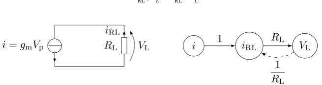
RL RL
: ; L: L
[image:9.595.210.538.81.168.2]i= i V =i ⋅R
Figure 11. Second subcircuit (left) of the CX-circuit is simplified by r0 and SFG (right) of the circuit.
From the definitions, the signal flow graph for the circuit of Figure 11 (left) can be constructed. The dashed edges describe the identity of the signal flow graph. With the help of the circuit from Figure 11, the signal flow graph of the second subcircuit can be determined much more easily. In reality, however, the total current i of the source does not flow through the load resistor RL. In order for the entire current i to flow through the load resistor RL, the resistance r0 would have to be infinite. But since the resistance r0 is not infinite, a small fraction of the source current flows through it. The current iRL through the load resistor RL can be adjusted by a suitable choice of the resistor r0. This allows the node rule to be set up.
RL: r0
i = −i i
The current
i
RL generates the voltage VL at the load resistor RL, which is equal to the magnitude of the voltage falling to r0. This relationship can be understood by means of the mesh rule. The voltage across the resistor r0 produces the current ir0 which acts on the current iRL through a negative feedback. In summary, the node, mesh rule and the material equations for the second subcircuit can now be set up.RL r0 r0 0
0
1
: ; : ;
i i i i V
r
= − = ⋅
L : 0; L: RL L
V =V V =i ⋅R
If the signal flow graph of the simple circuit is extended by the nodes V0 and
r0
i using the above equations, the signal flow graph of the second subcircuit will result, Figure 12. The material equations can be inverted. In reality, not all of the current i of the source flows through the load resistor RL: Thus, if the total current i flows through the load resistor RL, the resistance r0 would be infinite. But the resistance r0 being not infinitely large, a small portion of the source current flows through it. The current iRL through the load resistor RL can be adjusted by the appropriate choice of resistance r0 or reduced by this resistance. Thus, the nodes usually can be placed. The current iRL generates at the load resistor RL the voltage VL which is equal to the voltage drop across
0
DOI: 10.4236/cs.2017.811019 270 Circuits and Systems equations for the second subcircuit can now be set up. Extending the signal flow graph of the simple circuit around the edge
(
V i0,r0)
, yields the signal flow graph of the second subcircuit. The material equations can be inverted.Figure 12. (Above) Second subcircuit of CX-circuit and (below) SFG of the second subcircuit.
3.3. Signal Flow Graph of Total CX-Circuit
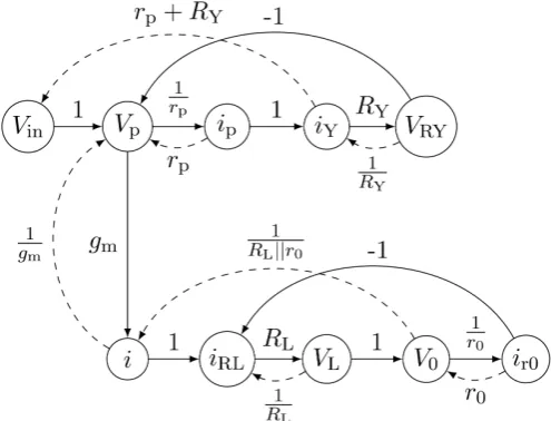
To make the signal flow graph of the CX-circuit, the individual subgraphs must be combined into a graph (Figure 13). The current source i is a voltage con-trolled current source. It is concon-trolled by the voltage Vp, the current is deter-mined by i=gm⋅Vp. Following the relationship between the current source i and the voltage Vp the two signal flow graphs can now be interconnected, Vin as source, iRL as sink, ip and VL as states.
Figure 13. Signal flow graph of the total CX-circuit for rp→ ∞
and RLr0.
3.4. Transfer Function of CX-Circuit
[image:10.595.250.498.449.638.2]Fig-DOI: 10.4236/cs.2017.811019 271 Circuits and Systems ure 13 using the SFG method. In order to find the transfer function, the signal flow graph from Figure 13 is to be simplified step by step so that the individual loops and paths leading to the solution are clearly visible.
• Elimination of the nodes i VY, RY, ,i V0 and ir0
Nodes
(
i VY, RY, ,i V i0,r0)
are eliminated by the associative law.• Elimination of the node iRL
The node ip is removed from the graph using the associative law. The node
RL
i is controlled by the rule for resolving feedback loops from the graph.
• Elimination of the reflexive edges and the node Vp
There is only one forward path from Vin to VL
m p 0
m L
V L
Y L p L 0 Y p 0
L Y 0 p 1 1 1
g r r
g R
A R
R R r R r R r r
R R r r ⋅ ⋅ = = ⋅ ⋅ + ⋅ + ⋅ + ⋅ + +
DOI: 10.4236/cs.2017.811019 272 Circuits and Systems flow graph (dashed 1-edge). Two signal flow graphs are always generated from one circuit, so that the signal flow graph already presented in previous sections corresponds to only half of the solution. The other half of the solution, the so-called identity, which is represented by a dashed edge, represents the inverse signal flow graph (SFG−1). If these two graphs are superposed with one another, so-called 1-edges are created at the node points. In Boolean algebra, this 1-edge is given the value 1, whereas this value can be identified with a zero in the field algebra.
Example: We want to check the 1 edge of the node Vp.
Now we look at all incoming and outgoing edges of this node of Figure 13, all other nodes and edges can be eliminated as well as dashed edges with material equations. Because material equations give us 1-edges, we do not use this to check. First we simplified Figure 13 as follows.
Then we look for incoming and outgoing edges within the loops. There are 2 loops, VP→ →ip iY→VRY→VP and VP→ →ip iY →Vin→VP , they are marked with diferent lines.
The nodes
(
i i Vp, ,Y RY)
are eliminated by the associative law. This gives the following signal flow graph.DOI: 10.4236/cs.2017.811019 273 Circuits and Systems elimination of the reflexive edges of Vin. It gives us the 1 edge of the node Vp.
And finally our SFG is checked. Analogously we can use this proof method for all nodes.
4. Conclusion
DOI: 10.4236/cs.2017.811019 274 Circuits and Systems
References
[1] Prasad, R. (2014) Fundamentals of Electrical Engineering. 3 rd Edition, PHI Learn-ing Private Limited, New Delhi.
[2] Palumbo, G. and Pennisi, S. (2007) Feedback Amplifiers: Theory and Design. Springer Science and Business Media, Berlin.
[3] Dorf, R.C. and Bishop, R.H. (2011) Modern Control Systems Solution Manual. Pearson Studium, London.
[4] Mason, S.J. (1956) Feedback Theory—Further Properties of Signal Flow Graphs.
IEEE, 44, 920-926. https://doi.org/10.1109/JRPROC.1956.275147
[5] Levine, W.S. (1996) The Control Handbook. CRC and IEEE Press, Boca Raton. [6] Brzozowski, J.A. and McCluskey, E.J. (1963) Signal Flow Graph Techniques for
Se-quential Circuit State Diagrams. IEEE, EC-12, 67-76.
[7] Horowitz, L.M. (2013) Syntehsis of Feedback Systems. Academic Press INC, Lon-don.
[8] Fakhfakh, M., Pierzchala, M. and Rodanski, B. (2012) An Improved Design of VCCS-Based Active Inducators, Synthesis, Modeling. Analysis and Simulation Me-thods and Applications to Circuit Design (SMACD) 2012, Seville, 19-21 September 2012.