Design of Equal Precision Frequency Meter
Based on FPGA
*
Yi-Yuan Fang, Xue-Jun Chen
College of Electrical and Electronic Engineering, Shanghai University of Engineering Science, Shanghai, China Email: [email protected]
Received July 22, 2012; revised August 24, 2012; accepted September 3, 2012
ABSTRACT
To overcome the shortcoming that the traditional frequency measurement method does not meet the requirement of equal precision, a design method of equal precision frequency meter based on FPGA is proposed. The system modules are all realized in Altera’s FPGA chip EP2C35F672C8. Experimental results show that the system can measure fquencies with equal precision in the whole frequency range, and the measurement error is small. It achieves the re-quirement of equal precision measurements.
Keywords: FPGA; Equal Precision; Frequency Measurement
1. Introduction
Frequency measurement is one of the most basic and important method in electronic measurements. Frequency signals are strong anti-interference, easy to transmit, and can be measured with higher precision. Therefore, the study of frequency measurement method is important in the practical engineering applications. The commonly used frequency measurement methods are direct fre- quency measurement, direct period measurement, and equal precision frequency measurement, etc. Direct fre- quency measurement is the method that counts the pulse number N within time t, then calculates the pulse number per unit time, i.e., the frequency of measured signal. Di- rect period measurement is the method that first mea- sures the period T of the measured signal, then calculates the signal frequency by f = 1/T. However, these two me-thods will produce ±1 period error of the measured signal, and therefore have some limitations in practical applica-tions. According to the measurement principle, it is very easy to find that the frequency measurement method is suitable for high-frequency signal, and period measure-ment method is suitable for low-frequency signal, how-ever, both can not take into account the requirement of equal precision measurement of high and low frequencies [1]. The maximum advantage of equal precision fre- quency measurement method compared to other fre- quency measurement methods is that it can achieve the equal precision in the entire frequency range, and have nothing to do with the size of the signal frequency.
2. Principle of Equal Precision Frequency
Measurement
The equal precision frequency measurement is also known as multi-cycle synchronous frequency measure- ment method. Its most prominent feature is that the ac- tual gate time is not a fixed value, but a value related with the measured signal, it is exactly an integer multiple of the measured signal period. Within the time allowed counting, we count pulse numbers of the standard signal and the measured signal at the same time, then derive the frequency of the measured signal through mathematical formula. As the gate time is an integer multiple of the measured signal period, this eliminates the ±1 period error of the measured signal, however, it will produce the ±1 period error of the standard signal [2]. The schematic diagram of equal precision measurement is shown in
Figure 1.
First, the control circuit gives out the gate signal, but the counter does not start counting until the rising edge of the measured signal comes. Then, the two counters start counting the pulse numbers of the measured signal and the standard signal respectively, and end counting until the falling edge of the measured signal, thus com- plete one measurement process. The counter’s opening and ending is completely synchronized with the mea- sured signal.
Figure 1 shows that the actual gate time is not a fixed value, it is exactly an integer multiple of the measured signal period, and it is synchronized with the measured signal. This eliminates the ±1 period error of the mea- sured signal. From the principle of frequency measure
*This work is supported by the Ph.D. Fund of Shanghai University of
Standard signal fs
Measured signal fx
Pre-gate T0
Count value Ns
Sync gate T T
[image:2.595.61.287.261.474.2]Count value Nx
Figure 1. Schematic diagram of equal precision measure- ment.
ment, we can obtain:
x s
x s
N N
T
f f
(1)
After deformation, we obtain:
x
x s
s
N
f f
N
(2)
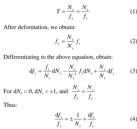
Differentiating to the above equation, obtain:
2
d s d x d xd
x x s s
s s
f N N
s s
f N f N
N N
f
N (3)
For dNx = 0, dNs = ±1, and x s
x s
N N
f f
Thus:
dx 1 ds
x s s
f f
f N f (4)
From (4) we can see: the measurement error has noth- ing to do with the frequency of the measured signal, only related with the gate time and frequency of standard sig- nals, namely, the equal precision measuring was achi- eved within the measured frequency band. The longer the gate time T and the higher the standard frequency fs, the
smaller relative error of the measured frequency. The relative error of standard frequency is dfs/fs. Because the
stability of the crystal is very high, therefore, the relative error of the standard signal is very small, and can be ig- nored.
3. Implementations of Equal Precision
Frequency Meter
The core idea of equal precision measurement is how to ensure the actual gate time is an integer multiple of the measured signal cycle. This requires the design to estab- lish a certain relationship between the actual gate time and the measured signal [3]. Based on this idea, the de- sign lets the rising edge of the measured signal as the drive signal for the gate opening and closing. Only when
the rising edge of the measured signal reaches, the state of the pre-gate T0 is latched, so that the cycles of the
measured signal during the actual measurement gate (i.e. synchronous gate T) is an integer. The block diagram of equal precision frequency is shown in Figure 2.
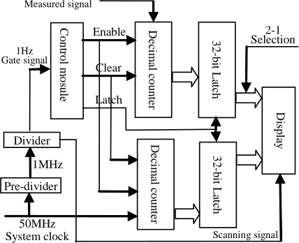
In Figure 2, the preset GATE signal is produced by a timing module in FPGA. Here the length of the preset gate signal is 1 s [4]. CNT1 and CNT2 are two controlled 32-bit high-speed counters. CNT1_ENA and CNT2_ ENA are their count enable terminals respectively. The reference frequency signal fs is input to CNT1_CLK. The
measured signal fx is input to CONT2_CLK, and also
connected to the clk of D flip-flop. During measurement, the timing module in FPGA generates preset GATE sig-nal. When GATE is in high level, and at the rising edge of fx, the 2 counters are triggered and start to count the
reference signal and the measured signal respectively. The condition for closing the counting gate is: GATE is low, and at the rising edge of fx. If in an actual gate time Tx, the count value of the measured signal is Nx, and the
count value of the standard signal is Ns, then by formula
(2), the frequency of measured signal fx can be calculated: fx = (Nx/Ns)*fs. For example, the counts of standard signal
and measured signal are 220 and 11, according to equa-tion (2), if the standard signal frequency is 20 MHz, then the measured signal frequency equals (11/220) × 20 MHz = 1 MHz.
3.1. System Design
The 50 MHz clock in the development platform is se- lected as the system clock of this experiment. The gate time is taken as 1 s (obtained by dividing the system clock). The enable signal TSTEN is a periodic signal with pulse width of 1 s, which is used to synchronize the two decimal counters CNT10. The counter is enabled when TSTEN is high, and disenabled when it is low. During the disenabled period, a rising edge of the latch signal LOAD is needed to latch the count value of the previous second into a 32-bit REG32B. The count value is translated by the decoder and displayed stable by seven-segment display. After latching, the counter is
CNT1
CNT1_CLK
CNT1_ENA
CLR D flip-flop
MUX
64-8 COUNT1[31,0]
CNT2 CNT2_CLK
CNT2_ENA
CLR COUNT2[31,0]
D Q
CLR Standard signal fs
Measured signal fx GATE
CLR
32 32
[image:2.595.312.535.603.715.2]Sel[2…0] Databus [7…0]
cleared by the clear signal CLR_CNT, and prepared for the next counting.
The frequency number Nx of the measured signal fx is
obtained by the cascade of eight decimal counter CNT10, and so does the standard signal frequency Ns. The com-
pleted count data is sent to the latch module REG32B for saving.
In this study, the system development platform pro- vides eight seven-segment displays, it can display up to 99,999,999. Therefore, the measurement range is 0 - 100 MHz. The display module is represented by eight 4-bit binary code (BCD code). It outputs the data of the latch (REG32B) to the display module, and displays it by the seven-segment LED. Data latch is to ensure that the sys- tem can stabilize the display data. The decoder driver cir- cuit is used to convert the binary count results into deci- mal results which can be displayed with seven-segment LED.
The system block diagram is shown in Figure 3. It mainly consists of six modules, namely: source module, signal selection module, control module, counting mo- dule, latch module and decoding display module.
3.2. Module Design and Function Simulation
3.2.1. Source Module
[image:3.595.307.539.85.156.2]The source module includes a pre frequency division module, and a multi frequency division module. In this paper, they are implemented with VHDL language. The pre frequency division module divides the input system clock (50 MHz) to generate a 1MHz clock frequency signal. Its timing simulation is shown in Figure 4. From
Figure 4, we can see a 1 MHz clock frequency is gene- rated by dividing the 50 MHz system clock with 50, which achieving the desired effect of the design.
The frequency divider module CNT has the function of generating variety of signals. Its main function is to
C
o
nt
ro
l m
o
su
le
D
eci
ma
l co
u
n
te
r
D
eci
ma
l co
u
n
te
r
32
-b
it L
atc
h
Di
sp
la
y
32
-b
it L
atc
h
50MHz System clock
Enable
Latch Clear
Measured signal
2-1 Selection
1MHz
Scanning signal
Divider
Pre-divider
[image:3.595.65.279.539.713.2]1Hz Gate signal
Figure 3. System block diagram.
Figure 4. Simulation of pre frequency division.
produce a gate signal with 1 s pulse width, a 7812 Hz scanning signal, and other desired test signals, including 500 KHz, 125 KHz, 31250 Hz, 7812 Hz, 1953 Hz, 488 Hz, and 1 Hz output frequencies. The input signal CLK is 1 MHz, the 1 Hz output signal freq1 is sent to the con- trol module, and the 7812 Hz output frequency is used as the input scanning signal of the display module. The oth-er frequencies are used as test signals. The simulation of the frequency divider is shown in Figure 5.
3.2.2. Control Module
The role of the control module is to produce a variety of required control signals for measuring frequency. Its in- put clock is 1 Hz, measuring the frequency once every two clock cycles. The input terminal CLK is connected to the output freq 1 of the divider CNT. The control mo- dule generates three control signals, respectively, CLR_ CNT TSTEN, and LOAD. The CLR_CNT signal is used to reset the counter at the beginning of each counting to clear the last count result, which is connected to CLR of the counter CNT10, high level effective, and sustains half a clock cycle. TSTEN is the count enable signal, is connected to ENA of the counter CNT10. At the rising edge of TSTEN, the count module starts to count the frequency of the input signal. The counting time is ex- actly one clock cycle (i.e. one unit time 1 s). The count value among this time is the signal frequency. The output terminal LOAD is connected to the latch’s input terminal LOAD. The simulation diagram of the control module is shown in Figure 6.
In the figure, the control signal clock CLK is taken as 1 Hz, therefore, the pulse width of TSTEN is just 1 s, which can be used as a gate signal. The figure also shows that the enable signal TETEN lasts 1 s in high level be- fore the counting finished, then its opposite latch signal LOAD produces a rising edge, and after 0.5 s, the clear signal CLR_CNT produces a rising edge.
3.2.3. Decimal Counter
Figure 5. Simulation of frequency divider.
Figure 6. Simulation of control module.
nal and asynchronous clear terminal for the control mo- dule to control it.
The reset terminal CLR of CNT10 is connected to the output terminal CLR_CNT of TESTCTL, its enable ter- minal ENA is connected to the TSTEN terminal of TESTCTL, and its output terminal CQ[3..0] is connected to DIN[31..0] of the latch. The simulation is shown in
Figure 7.
The function of this module is to realize a decimal counter with enable terminal. The counter works pro- perly only when the enable signal is at high level. The counter pluses one when each rising edge of the clock comes. When counting to 10, the counter is cleared, while a carry on signal is produced, which is only a pulse signal. Once the count changes from 10 to 1, the pulse signal immediately goes low. Also the counter has a clear signal. Once the clear signal is at high level, the counter is cleared immediately. In this design, two signals need to be counted, so there are two 32-bit data output.
3.2.4. 32-Bit Latch
The latch module is mainly composed by the master- slave flip-flop. It plays the role of data protection to en- sure its stability before being displayed. After the count module completes counting, the latch module latches the count value into the register at the rising edge of the load signal; then outputs to the display module, and save the data until the next trigger or reset.
The latch’s input terminal LOAD is connected to the output terminal LOAD of the control module TESTCTL; its input terminal DIN[31..0] is connected to output ter- minal CQ[3..0] of the counter CNT10, and its output ter- minal DOUT[31..0] is connected to the In[3..0] terminals of the Display module.
Figure 7. Simulation of CNT10.
3.2.5. Seven-Segment LED Display Module
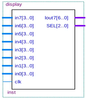
Seven-segment LED has segment code and location code. Segment code is used to convert the 4-bit binary input number into the corresponding 8-bit segment code for LED display through a decoding circuit. Location code is used to enable the LED. For the common cathode LED, low level enables. This design uses a 3-bit circulating selector to enable each LED in turn. Because there are eight LED need to display simultaneously, we must cy- clic scan each LED, and input the 8-bit segment code corresponding to the required display data while enable each LED. Although the 8 LED display in turn, but for the sake of visual resolution, it looks the 8 LED work simultaneously.
[image:4.595.57.289.223.308.2]The block diagram of display module is shown in
Figure 8. Where In0 - In7 is connected to DOUT[31..0] of the latch, and output terminals are connected to the segment and select pins of LED.
All modules in the design are implemented in Altera’s FPGA chip EP2C35F672C8. The outputs of the counting modules are two 32-bit data. These two 32-bit data is output by the latch. The counting numbers Nx and Ns are
converted into the actual frequency value according to the equal precision frequency Formula (2).
4. Experimental Results and Error Analysis
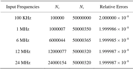
In experiment, the 50 MHz high stability quartz crystal was used as the standard signal. The measured results and relative errors are shown in Table 1.
in7[3..0]
in6[3..0]
in5[3..0]
in4[3..0]
in3[3..0]
in2[3..0]
in1[3..0]
in0[3..0]
clk
lout7[6..0]
SEL[2..0]
display
[image:4.595.353.492.560.719.2]inst
Table 1. Experimental result and relative errors.
Input Frequencies Nx Ns Relative Errors
100 KHz 100000 50000000 2.000000 × 10⁻⁸
1 MHz 1000007 50000350 1.999986 × 10⁻⁸
6 MHz 6000044 50000365 1.999985 × 10⁻⁸
12 MHz 12000077 50000320 1.999987 × 10⁻⁸
24 MHz 24000154 50000320 1.999987 × 10⁻⁸
The results show that the relative error is less than 2 × 10⁻⁸ within the experimental frequency range 100 KHz to 24 MHz. The measurement errors distribute in the same order of magnitude, which achieves the purpose of equal precision measurement.
5. Conclusion
This paper describes the principles of equal precision measuring, proposes the design method of precision fre- quency meter based on FPGA. Because the design can eliminate the ±1 count error of the measured signal,
therefore, greatly improve the precision, and can achieve equal precision measurement without changing the mea- suring range in the whole frequency range. The results show that the relative error is very small and constant in the whole measurement range. At the same time, the de- sign has great flexibility, high integration, with some reference value. Especially in the field of electronic de- sign, where SOC technology has recently become in- creasingly mature, this design shows great significance.
REFERENCES
[1] S. Pan, “VHDL Practical Tutorial,” Xi’an Electronic In-dustry Press, Xi’an, 2002.
[2] Z.-H. Xia, “Realization of Equal Precision Frequency Meter,” Electronic Design Engineering, Vol. 18, No. 6, 2010, pp. 177-182.
[3] Z. D. Mao, “Design of Equal Precision Frequency Meter with FPGA,” Electronic Measurement Technology, Vol. 29, No. 4, 2007, pp. 85-86.