STUDY OF STRUCTURAL AND OPTICAL PROPERTIES OF CD
CHEMICAL SPRAY PYROLYSIS METHOD
1
Ziad T. Khodair,
1Department of Physics, College of Science, Uni
2Diyala General Directorate of Education, Diyala, Iraq
ARTICLE INFO ABSTRACT
In this study
strate at (400 ºC) by chemical spray pyrolysis technique using cadmium acetate as the Cd source. effect of Cr doping on structural and optical properties has been investigated. XRD invest showed that all the films were polycrystalline in nature and had a cubic structure with preferred orientation along (111) plane for all doping percentages. It was found that doping with (Cr) led to decrease in the intensity of (111) peak and the a
increases. The optical
spectrum and it increases with Cr
2.63, 2.65, 2.67 and 2.71 eV) for different values of Cr percentage respectively. The absorption coefficient, reflectance, and Urbach tail were calculated also.
Copyright © 2014 Ziad T. Khodair et al. This is an open access article
use, distribution, and reproduction in any medium, provided the original work is properly cited.
INTRODUCTION
Transparent conductive oxide (TCO) films have been extensively studied because of their use in semiconductor device technology. CdO thin films have high transparency in the visible region of the electromagnetic spectrum and show degenerate n-type conductivity mainly due to oxygen vacancies, high carrier concentration contributed by shallow donors resulting from self non-stoichiometry
2014; Khan et al., 2010). In recent years, transparent conductive oxide (TCO) layers have attracted much attention due to their high optical transmittance and low resistivity. They have been obtained by different research groups because they have potential applications in photovoltaic solar cells, phototransistors, liquid crystal displays, optical heaters, gas sensors, transparent electrodes, and other optoelectronic devices (Ali Yıldırım and Ates 2009; Zheng
Inherently CdO is an n-type semiconductor with optical ba gap varying from 2.2 to 2.9 eV. Currently, nanostructured materials are not only in the forefront of the hottest studies on fundamental materials, but are also gradually entering the daily lives of people. One-dimensional (1D) metal oxide semiconductor nanostructures, such as nanorods and nanowires have attracted wide attention for their potential applications
*Corresponding author: Nabeel A. Bakr
Department of Physics, College of Science, University of Diyala, Diyala, Iraq.
ISSN: 0975-833X
International Journal of Current Research
Vol. 6, Issue, 09, pp.838
Article History:
Received 25th June, 2014
Received in revised form 06th
July, 2014 Accepted 20th
August, 2014 Published online 18th
September,2014
Key words:
CdO thin films, Chemical Spray Pyrolysis, Optical Properties, X-ray diffraction, Cr Doping
RESEARCH ARTICLE
STUDY OF STRUCTURAL AND OPTICAL PROPERTIES OF CD
(1-X)Cr
XO THIN FILMS PREPARED BY
CHEMICAL SPRAY PYROLYSIS METHOD
Ziad T. Khodair,
1*Nabeel A. Bakr and
1,2Rahem Ahmed Ali
Department of Physics, College of Science, University of Diyala, Diyala, Iraq Diyala General Directorate of Education, Diyala, Iraq
ABSTRACT
In this study, undoped (CdO) films and Cr doped (with 2,4,6 and 8 wt%) were deposited on glass sub strate at (400 ºC) by chemical spray pyrolysis technique using cadmium acetate as the Cd source. effect of Cr doping on structural and optical properties has been investigated. XRD invest showed that all the films were polycrystalline in nature and had a cubic structure with preferred orientation along (111) plane for all doping percentages. It was found that doping with (Cr) led to decrease in the intensity of (111) peak and the average grain size decreases as (Cr) doping percentage increases. The optical characterization of the filmshave good transmittance in the visible region of spectrum and it increases with Cr-doping, with increase in direct band gap (2.4 eV for undoped 2.63, 2.65, 2.67 and 2.71 eV) for different values of Cr percentage respectively. The absorption coefficient, reflectance, and Urbach tail were calculated also.
is an open access article distributed under the Creative Commons Attribution License, which permits unrestricted use, distribution, and reproduction in any medium, provided the original work is properly cited.
Transparent conductive oxide (TCO) films have been extensively studied because of their use in semiconductor device technology. CdO thin films have high transparency in electromagnetic spectrum and show type conductivity mainly due to oxygen vacancies, high carrier concentration contributed by shallow stoichiometry (Sahin et al., . In recent years, transparent conductive oxide (TCO) layers have attracted much attention due to their high optical transmittance and low resistivity. They have been obtained by different research groups because they ltaic solar cells, phototransistors, liquid crystal displays, optical heaters, gas sensors, transparent electrodes, and other optoelectronic Zheng et al., 2010). type semiconductor with optical band gap varying from 2.2 to 2.9 eV. Currently, nanostructured materials are not only in the forefront of the hottest studies on fundamental materials, but are also gradually entering the daily dimensional (1D) metal oxide nanostructures, such as nanorods and nanowires
potential applications
Department of Physics, College of Science, University of Diyala,
in device and interconnect integrations in nano and molecular electronics (Zaien and Ahmed, Z. Hassan
techniques such as sol–gel, spray pyrolysis, ion beam sputtering, magnetic sputtering, and pulsed laser deposition have been used for deposition of pure and doped CdO films (Serbetc et al., 2012). In the present paper, we report the effect of (Cr) doping on the optical and structural properties of CdO films prepared by chemical spray pyrolysis technique.
Experimental procedure
Chemical spray pyrolysis technique was used to deposit undoped and Cr-doped (CdO) films on glass substrates at temperature of (400 ºC). In the preparation of (CdO) films aqueous solution of (0.3M) cadmium acetate (Cd(CH
2H2O) was mixed with distilled water by using magnetic
stirrer for (15min). To achieve Cr-doping aqueous solution of (0.3M) chromium chloride (CrCl
concentrations of (2, 4, 6, 8) wt% and mixed with precursor solution. The resultant solution was sprayed on glass su kept at (400 ºC). Other deposition conditions
spray nozzle substrate distance (30 cm), spray time (8 s), spray interval (2 min) and pressure of the carrier gas (1.5 bar) were kept constant for each concentration. Optical transmitta spectra in the wavelength of (300-900) nm
using UV-VIS-NIR spectroscopy (Shimadzu,UV
the X-ray diffraction patterns were obtained in a (Shimadzu
XRD-6000) goniometer using copper target
(Cu Kα, 1.5418 Å).
International Journal of Current Research
Vol. 6, Issue, 09, pp.8384-8389, September,2014
OF CURRENT RESEARCH
O THIN FILMS PREPARED BY
Ahmed Ali
versity of Diyala, Diyala, Iraq
and Cr doped (with 2,4,6 and 8 wt%) were deposited on glass sub strate at (400 ºC) by chemical spray pyrolysis technique using cadmium acetate as the Cd source. The effect of Cr doping on structural and optical properties has been investigated. XRD investigations showed that all the films were polycrystalline in nature and had a cubic structure with preferred orientation along (111) plane for all doping percentages. It was found that doping with (Cr) led to verage grain size decreases as (Cr) doping percentage have good transmittance in the visible region of doping, with increase in direct band gap (2.4 eV for undoped to 2.63, 2.65, 2.67 and 2.71 eV) for different values of Cr percentage respectively. The absorption
distributed under the Creative Commons Attribution License, which permits unrestricted
device and interconnect integrations in nano and molecular Ahmed, Z. Hassan 2012). Different gel, spray pyrolysis, ion beam sputtering, magnetic sputtering, and pulsed laser deposition sition of pure and doped CdO films In the present paper, we report the effect of (Cr) doping on the optical and structural properties of CdO films prepared by chemical spray pyrolysis technique.
Chemical spray pyrolysis technique was used to deposit doped (CdO) films on glass substrates at temperature of (400 ºC). In the preparation of (CdO) films aqueous solution of (0.3M) cadmium acetate (Cd(CH3COO)2.
d water by using magnetic doping aqueous solution of (0.3M) chromium chloride (CrCl3.6H2O) with various
, 4, 6, 8) wt% and mixed with precursor solution. The resultant solution was sprayed on glass substrate kept at (400 ºC). Other deposition conditions are as follows: spray nozzle substrate distance (30 cm), spray time (8 s), spray the carrier gas (1.5 bar) were Optical transmittance 900) nm were recorded by NIR spectroscopy (Shimadzu,UV-1800) and ray diffraction patterns were obtained in a (Shimadzu
6000) goniometer using copper target
RESULTS AND DISCUSSION
Structural analysis
[image:2.612.62.295.126.260.2]XRD patterns of the undoped and Cr–doped CdO films are shown in Figure 1.
Fig. 1. X–ray diffraction patterns of undoped and Cr-doped CdO films
The patterns indicate that all of the films have a polycrystalline with cubic face centered crystal structure (Dakhel 2010; Yuankun Zhu et al., 2013). For the films, the main characteristic peaks are assigned to the (111), (200), (220) and (311) planes. The relatively stronger peak intensity indicates preferential (111) orientation of the films. Similar behavior has also been reported by other studies (Aydın et al., 2012; Akyuz et al., 2010). The average grain size for the films can be determined using Williamson-Hall formula (Prabhu et al., 2013) shown below:
βhklcos=Kλ/D+4Ssin
where βhkl isfull width of half maximum D is the average
grain size,k is constant and was assumed to be equal to 0.9, λ is wavelength for Cu target for XRD instrument,is Bragg’s angle for all peaks, and S is the microstrain of the film. The average grain size for all films are also calculated by Scherrer formula according relation (Zaien et al., 2011):
D = (0.94 λ) / (β cosθ) ………..(2)
The grain size decreases regularly upon increasing the Cr-concentration and peaks shift towards higher angles were also noted from XRD results which indicate the compression in unit cell. This may be due to the lower ionic radius of Cr+3 (0.0615 nm) compared with Cd+2 ionic radius (0.095nm) (Dakhel and Hamad 2013). The texture coefficient (TC) represents the
texture of the particular plane; in which greater than unity values imply that there are numerous of grains in that particular direction. The different texture coefficients TC(hkl) have been
calculated from the X-ray data using the well-known formula (Seval Aksoy et al., 2009):
……….(3)
where I(hkl) is the measured relative intensity of a plane (hkl), Io(hkl) is the standard intensity of the plane (hkl) taken from
the JCPDS data, N is the reflection number and n is the number of diffraction peaks. The results indicate that (Tc) decreases with increasing the doping percentage and the calculated values of TC(hkl) are greater than unity, especially
[image:2.612.316.552.204.301.2]those corresponding to (111) plane. This indicates that the respective films have the largest preferred crystallographic orientation along the (111) diffraction planes. All these results are shown in Table 1.
Table 1. Structural parameters of the undoped and Cr-doped CdO films
Cd0.92Cr0.08O
Cd0.94Cr0.06O
Cd0.96Cr
0.04O
Cd0.98Cr0
.02O CdO pure Sample 111 111 111 111 111 hkl 33.0298 33.0203 33.0481 33.0253 32.9958 2Ɵ 2.70980 2.71056 2.70834 2.71016 2.71251 d 0.5800 0.5110 0.4767 0.4500 0.4032 FWHM 14 16 17 18 21
DavScherrer
7 9
10 11 13
Dav W-H
4.6935 4.6948 4.6909 4.6941 4.6982 Lattice constant 1.16 1.30 1.31 1.41 1.47 Tc Optical analysis
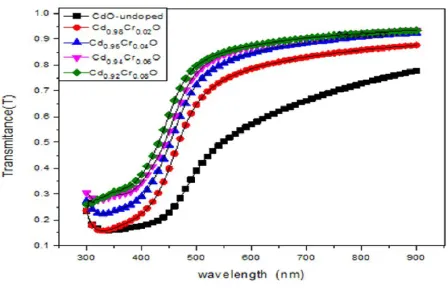
Optical absorption spectra of the films in spectral range of (300-900 nm) were determined by using UV–visible spectrophotometer. The analysis of the dependence of absorption coefficient on photon energy in the high absorption regions is performed to obtain the detailed information about the energy band gaps of the films (Sahin et al., 2014). The transmittance spectra of the films are shown in Figure (2). These spectra show that adding (Cr) to (CdO) improves the transmittance for all deposited samples. The transmittance of undoped films was (51%) at (550 nm) and after doping, the transmittance increases up to (80%) at (550 nm).
Fig. 2. Transmittance spectra of the undoped and Cr–doped CdO films
The optical transition involved in the absorption process and
[image:2.612.318.542.463.608.2]
………(4)
[image:3.612.63.296.191.344.2]Fig (3) shows the relation between (α) and photon energy. The variation of the optical absorbance with wavelength is shown in Fig (4). Calculated values of absorption coefficient are in the order of (104) cm-1 which can be attributed to the direct electronic transition. From Fig (4) it is shown that absorbance decreases with increasing Cr doping concentration and a sharp decrease is observed near the band edge.
[image:3.612.58.298.195.549.2]Fig. 3. Absorption coefficient of the undoped and Cr–doped CdO films
Fig. 4. Absorbance spectra of the undoped and Cr–doped CdO films
The optical energy band gap (Eg) is given by the classical relation (Tauc 1974):
αhν=A(hν–Eg) r
……….(5)
Where α is the absorption coefficient, hν is the photon energy, Eg is the optical band gap, A is a constant which does not depend on photon energy and r has four numeric values (1/2) for allowed direct, 2 for allowed indirect, 3 for forbidden direct
direct band gap was determined by plotting (αhν)2 vs. hν curves, with the extrapolation of the linear region to low energies.
From Figure (5), it was observed that the undoped films exhibit a band gap values of (2.40 eV) and the band gap value increases with increase in Cr-doping concentration (2, 4, 6, and 8) wt% and it is (2.63, 2.65, 2.67 and 2.71) eV respectively. The increase in the band gap energy is due to increase in free electron concentration in the films. The shift of the band gap with change in the carrier concentration can be explained by the Burstein-Moss shift (Fan et al., 2007). Reflectance curves of undoped and Cr-doped films are shown in Fig (6).
It can be seen that the reflectance of the films increases with increase in photon energy and begins to go down near the energies corresponding to the band gap. However the reflectance is higher in the undoped films compared to the Cr-doped films. The shift is related to the changes in the films characteristics. The width of the localized states available in the optical band gap of the films affects the optical band gap structure and optical transitions and it is called as Urbach tail, which is related directly to a similar exponential tail for the density of states of either one of the two band edges. The Urbach tail of the films can be determined by the following relation (Ilican et al., 2009):
………..(6)
where E is the photon energy, αo is constant, and Eu is the Urbach energy which
refers to the width of the exponential absorption edge.
Figure (7) shows the variation of (lnα) vs .photon energy for the films. This behavior corresponds primarily to optical transitions between occupied states in the valance band tail to unoccupied states at the conduction band edge. The EU value
was calculated from the slope of Figure (7) using relationship:
………(7)
The obtained EU values are given in Table (2). Urbach energy
values of the films decrease with increasing Cr-dopant. The EU
[image:3.612.63.296.377.551.2]values change inversely with optical band gaps of films.
Table 2. Values of Urbach energy of the undoped and Cr-doped CdO films
Eu(meV)
Samples
553 CdO-undoped
382 Cd0.98Cr0.02O
365 Cd0.96Cr0.04O
324 Cd0.94Cr0.06O
[image:3.612.357.508.639.700.2]Fig. 6. Reflectance spectra of the undoped and Cr–doped CdO films
[image:5.612.75.542.241.715.2]Conclusions
In this study, undoped (CdO) films and Cr doped (with 2,4,6 and 8 wt%) were successfully deposited on glass substrates at (400 ºC) by chemical spray pyrolysis technique using cadmium acetate as the Cd source. XRD patterns of the undoped and Cr–doped CdO films indicate that all of the films are polycrystalline with cubic face centered crystal structure. The main characteristic peaks are assigned to the (111), (200), (220) and (311) planes. The grain size decreases regularly upon increasing the Cr-concentration and peaks shift towards higher angles were also noted from XRD results which indicate the compression in unit cell. This may be due to the lower ionic radius of Cr+3 (0.0615 nm) compared with Cd+2 ionic radius (0.095nm). The transmittance spectra of the films show that adding (Cr) to (CdO) improves the transmittance for all deposited samples. The transmittance of undoped films was (51%) at (550 nm) and after doping the transmittance increases up to (80%) at (550 nm). It was observed that the undoped films exhibit a band gap values of (2.40 eV) and the band gap value increases with increase in Cr-doping concentration (2, 4, 6, and 8) wt% and it is (2.63, 2.65, 2.67 and 2.71) eV respectively. The increase in the band gap energy was attributed to the increase in free electron concentration in the films. The shift of the band gap with change in the carrier concentration could be explained by the Burstein-Moss shift.
REFRENCES
Akyuz I., S. Kose, F. Atay, V. Bilgin, 2010. “Preparation and characterization of inum-incorporated cadmium oxide films” Materials Science in Semiconductor Processing 13, 109-114.
Ali Yıldırım M. and A. Ates, 2009. “Structural, optical and electrical properties of CdO/Cd(OH)2 thin films grown by
the SILAR method,” Sensors and Actuators A, 155, 272– 277.
Aydın C., Omar A. Hartomy, A. A. Ghamdi, F. Al-Hazmi, I. S. Yahia, F. El-Tantawy, 2012. “Controlling of crystal size and optical band gap of CdO nanopowder semiconductors by low and high Fe contents” J Electroceram, 29, 155-162.
Dakhel A. A., H. Hamad 2013. "The structural, electrical, and optical of hydrogen chromium-doped CdO films". Journal of Solid State Chemistry, 208, 14-19.
Dakhel A.A., 2010. “Electrical and optical properties of iron-doped CdO,Thin Solid Films” 518, 1712–1715.
Fan X.Y., Z.G. Wu, G.A. Zhang, C. Li, B.S. Geng, H.J. Li, 2007. “Ti-doped copper nitride films deposited by cylindrical magnetron sputtering” Journal of Alloys and Compounds 440, 254-258.
Ilican S., M. Caglar, Y. Caglar, F. Yakuphanoglu, 2009. “CdO:Al films deposited by sol-gel process: a study on their structural and optical properties” Optoelectronics and advanced materials-Rapid communications, 3, 2, 135-140. Khan M.K.R., M. Azizar Rahman, M. Shahjahan, M. Mozibur Rahman,” 2010. Effect of Al-doping on optical and electrical properties of spray pyrolytic nano-crystalline CdO thin films, Current Applied Physics, 10, 790–796. Prabhu Y. T., K. Venkateswara Rao, V. Sesha Sai Kumar, B.
Siva Kumari. 2013. "X- ray Analysis of Fe doped ZnO Nanoparticles by Williamson-Hall and Size- Strain Plot" International Journal of Engineering and Advanced Technology (IJEAT),4, 2249- 8958.
Sahin B., F. Bayansala, M. Yukselc, N. Biyiklib,” 2014. Effect of coumarin concentration on the physical properties of CdO nanostructures” J. Ceramics International, 40, 5237-5243.
Serbetc Z. ¸ R. K. Gupta, F. Yakuphanoglu, 2012. "Preparation and characterization of nanorods Sb doped
CdO films by sol–gel technique”, J. Sol-Gel Sci Technol, 61, 477–483.
Seval Aksoy, Yasemin Caglar, Saliha Ilican, Mujdat Caglar, 2009. Effect of heat treatment on physical properties of CdO films deposited by sol–gel method” International Journal of Hydrogen Energy, 3, 5191-5198.
Tauc, J. 1974. “Amorphous and Liquid Semiconductors,” Plenum, London.
Yuankun Zhu, Rueben J. Mendelsberg, Jiaqi Zhu, 2013. “Transparent and conductive indium doped cadmium oxide thin films prepared by pulsed filtered cathodic arc deposition”,Applied Surface Science 265, 738– 744. Zaien M., K. Omar, Z. Hassan, 2011. “Synthesis of
dendrite-like petals of CdO nanostructure” Optoelectronics and advanced materials-Rapid communications, 5, 9, 982- 984.
Zaien M., N. M. Ahmed, Z. 2012. Hassan, growth of cadmium oxide nanorods by vapor transport, J. Chalcogenide Letters, 9, 3, 115 – 119.
Zheng B. J., J. S. Lian, L. Zhao, and Q. Jiang, 2010. “Optical and electrical properties of In-doped CdO thin films fabricated by pulse laser deposition,” Applied Surface Science, 256, 9, 2910–2914.