Int. J. Adv. Res. Sci. Technol. Volum e 3, Issue 4, 2014, pp.219-223.
International Journal of Advanced Research in
Science and Technology
journal homepage: w w w .ijarst.com
IS S N 2319 – 1783 (Print) IS S N 2320 – 1126 (Online)
On-Chip Bus Designing with the Interface of Open Core Protocol
Pathivada V J Raj Kumar* andKurada Phaneedra
Department of ECE, Vizag Institute of Technology, Visakhapatnam, Andhra Pradesh, India.
*Corresponding Author’s Email: [email protected]
A R T I C L E I N F O A B S T R A C T
Article history:
Received Accepted Available online
20 Nov. 2014 19 Dec. 2014 25 Dec. 2014
As more and more IP cores are integrated into an SOC design, the communication flow between IP cores has increased drastically and the efficiency of the on-chip bus has become a dominant factor for the performance of a system. The on-chip bus design can be divided into two parts, namely the interface and the internal architecture of the bus. In this work we adopt the well-defined interface standard, the Open Core Protocol (OCP), and focus on the design of the internal bus architecture. We develop an efficient bus architecture to support most advanced bus functionalities defined in OCP, including burst transactions, lock transactions, pipelined transactions, and out of-order transactions. We first model and design the on-chip bus with transaction level modeling for the consideration of design flexibility and fast simulation speed. We then implement the RTL models of the bus for synthesis and gate-level simulation. Experimental results show that the proposed TLM model is quite efficient for the whole system simulation and the real implementation can significantly save the communication time.
© 2014 International Journal of Advanced Research in Science and Technology (IJARST). All rights reserved.
Keywords:
AMBA AHB AXI
Open Core Protocol – International Partnership (OCP-IP)
Introducti on:
An SOC chip usually contains a large number of IP cores that communicate with each other through on -chip buses. As the VLSI process technology continuously advances, the frequency and the amount of the data communication between IP cores increase substantially. As a result, the ability of on chip buses to deal with the large amount of data traffic becomes a dominant factor for the overall performance.
The design of on-chip buses can be divided into two parts: bus interface and bus architecture. The bus interface involves a set of interface signals and their corresponding timing relationship, while the bus architecture refers to the internal components of buses and the interconnections among the IP cores. The widely accepted on-chip bus, AMBA AHB [1], defines a set of bus interface to facilitate basic (single) and burst read/write transactions. AHB also defines the internal bus architecture, which is mainly a shared bus composed of multiplexors. The multiplexer-based bus architecture works well for a design with a small number of IP cores. When the number of integrated IP cores increases, the communication between IP cores also increase and it becomes quite frequent that two or more master IPs would request data from different
slaves at the same time. The shared bus architecture often cannot provide efficient communication since only one bus transaction can be supported at a time.
Int. J. Adv. Res. Sci. Technol. Volum e 3, Issue 4, 2014, pp.219-223. and the whole system architecture. In this way, system
integration becomes much more efficient. Most of the bus functionalities defined in AXI and OCP are quite similar. The most conspicuous difference between them is that AXI divides the address channel into independent write address channel and read address channel such that read and write transactions can be processed simultaneously. However, the additional area of the separated address channels is the penalty.
Some previous work has investigated on-chip buses from various aspects. The work presented in [3] and [4] develops high-level AMBA bus models with fast simulation speed and high timing accuracy. The authors in [5] propose an automatic approach to generate high -level bus models from a formal channel model of OCP. In both of the above work, the authors concentrate on fast and accurate simulation models at high level but did not provide real hardware implementation details. In [6], the authors implement the AXI interface on shared bus architecture. Even though it costs less in area, the benefit of AXI in the communication efficiency may be limited by the shared-bus architecture.
In this paper we propose a high-performance on-chip bus design with OCP as the bus interface. We choose OCP because it is open to the public and OCP-IP has provided some free tools to verify this protocol. Nevertheless, most bus design techniques developed in this paper can also be applied to the AXI bus. Our proposed bus architecture features crossbar/partial-crossbar based interconnect and realizes most transactions defined in OCP, including 1) single transactions, 2) burst transactions, 3) lock transactions, 4) pipelined transactions, and 5) out-of-order transactions. In addition, the proposed bus is flexible such that one can adjust the bus architecture according to the system requirement.
One key issue of advanced buses is how to manipulate the order of transactions such that requests from masters and responses from slaves can be carried out in best efficiency without violating any ordering constraint. In this work we have developed a key bus component called the scheduler to handle the ordering issues of out-of-order transactions. We will show that the proposed crossbar/partial-crossbar bus architecture together with the scheduler can significantly enhance the communication efficiency of a complex SOC.
Another notable feature of this work is that we employ both transaction level modeling (TLM) and register transfer level (RTL) modeling to design the bus. We start from the TLM for the consideration of design flexibility and fast simulation speed. We then refine the TLM design into synthesizable and cycle-accurate RTL codes which can be synthesized into gate level hardware to facilitate accurate timing and functional simulation. The proposed bus has been employed in a multimedia SOC design and the results show that not only our TLM model has better simulation efficiency comparing to a bus obtained through a commercial ESL tool, but also our RTL on
-chip bus design performs much more efficient than the multiplexer-based buses or those without out-of-order feature in real SOC design.
The remainder of this paper is organized as follows. The various advanced functionalities of on -chip buses are described in Section 2. Section 3 details the hardware architecture of the proposed bus. Section 4 gives the experimental results which show the efficiency on both simulation speed and data communication. Conclusions are then drawn in Section 5.
On-chip bus functionalities :
We first describe the various bus functionalities including 1) burst, 2) lock, 3) pipelined, and 4) out-of-order transactions .
Burst transactions:
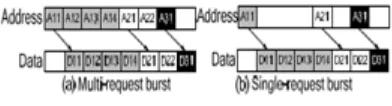
The burst transactions allow the grouping of multiple transactions that have a certain address relationship, and can be classified into multi-request burst and single-request burst according to how many times the addresses are is sued. FIGURE 1 shows the two types of burst read transactions. The multi-request burst as defined in AHB is illustrated in FIGURE 1(a) where the address information must be issued for each command of a burst transaction (e.g., A11, A12, A13 and A14). This may cause some unnecessary overhead. In the more advanced bus architecture, the single-request burst transaction is supported. As shown in FIGURE 1(b), which is the burst type defined in AXI, the address information is issued only once for each burst transaction. In our proposed bus design we support both burst transactions such that IP cores with various burst types can use the proposed on -chip bus without changing their original burst behavior.
Fig. 1: Burst transactions
Lock transactions:
Lock is a protection mechanism for mas ters that have low bus priorities. Without this mechanism the read/write transactions of masters with lower priority would be interrupted whenever a higher-priority master issues a request. Lock transactions prevent an arbiter from performing arbitration and assure that the low priority masters can complete its granted transaction without being interrupted.
Pipelined transactions (outstanding transactions):
Int. J. Adv. Res. Sci. Technol. Volum e 3, Issue 4, 2014, pp.219-223. latency. For example, D21 is sent right after A21 is
issued plus t. For a pipelined transaction as shown in Figure 2(b), this hard link is not required. Thus A21 can be issued right after A11 is issued without waiting for the return of data requested by A11 (i.e., D11-D14).
Fig. 2: Pipelined transactions
Out-of-order transactions:
The out-of-order transactions allow the return order of responses to be different from the order of their requests. These transactions can significantly improve the communication efficiency of an SOC system containing IP cores with various access latencies as illustrated in FIGURE 3. In FIGURE 3(a) which does not allow out-of-order transactions, the corresponding responses of A21 and A31 must be returned after the response of A11. With the support of out-of-order transactions as shown in FIGURE 3(b), the response with shorter access latency (D21, D22 and D31) can be returned before those with longer latency (D11-D14) and thus the transactions can be completed in much less cycles.
Fig. 3: Out-of-order transactions
Hardware Design of the On-Chip Bus:
The architecture of the proposed on-chip bus is illustrated in FIGURE 4, where we show an example with two masters and two slaves. A crossbar architecture is employed such that more than one master can communicate with more than one slave simultaneously. If not all masters require the accessing paths to all slaves, partial crossbar architecture is also allowed. The main blocks of the proposed bus architecture are described next.
Arbiter:
In traditional shared bus architecture, resource contention happens whenever more than one master requests the bus at the same time. For a cross bar or partial crossbar architecture, resource contention occurs
when more than one master is to access the same slave simultaneously. In the proposed design each slave IP is associated with an arbiter that determines which master can access the slave.
Fig. 4: traditional shared bus architecture
Decoder:
Since more than one slave exists in the system, the decoder decodes the address and decides which slave return response to the target master. In addition, the proposed decoder also checks whether the transaction address is illegal or nonexistent and responses with an error message if necessary.
FSM-M & FSM-S:
Depending on whether a transaction is a read or a write operation, the request and response processes are different. For a write transaction, the data to be written is sent out together with the address of the target slave, and the transaction is complete when the target slave accepts the data and acknowledges the reception of the data. For a read operation, the address of the target slave is first sent out and the target slave will issue an accept signal when it receives the message. The slave then generates the required data and sends it to the bus
where the data will be properly directed to the master requesting the data. The read transaction finally completes when the master accepts the response and issues an acknowledge signal. In the proposed bus architecture, we employ two types of finite state machines, namely FSM-M and FSM-S to control the flow of each transaction. FSM-M acts as a master and generates the OCP s ignals of a master, while FSM-S acts as a slave and generates those of a slave. These finite state machines are designed in a way that burst, pipelined, and out-or-order read/write transactions can all be properly controlled.
Scheduler:
Int. J. Adv. Res. Sci. Technol. Volum e 3, Issue 4, 2014, pp.219-223. Whether to favor in-order or out-of-order
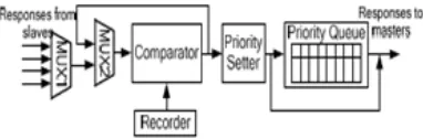
transactions is a design issue of the bus. In [7] it is stated that conventional bus scheduling algorithms tend to favor the in-order transactions, while the ordering mechanism proposed in [7] favors out-of order transactions. In our proposed scheduler, we reserve the flexibility of being in-order response first or out-of-order. Response first, which means that system integrators are allowed to select either order based on the applications. The architecture of the proposed scheduler is shown in FIGURE 5.
A multiplexer, MUX1, is used to solve the problem of Resource contention when more than one slave returns the responses to the same master. It selects the response from the slave that has the highest priority. The function of MUX2 will be des cribed shortly. The recorder shown in the figure is used to keep track of the ID of the target slave and the TagID of every out-of-order transaction. Whenever a response arrives, the comparator determines whether the ordering restriction is violated or not by comparing the ID of the target slave and TagID. If no ordering restriction is violated, the response is sent forward to the priority setter. If the restriction is violated, the response is sent backward to one of the inputs of MUX2, which is always a preferred input over the input from MUX1. The responses sent forward are given a priority, which is different from the slave priority, according to the TagID and are stored in the priority queue. For the transactions without TagID, which are regarded as in-order transactions, the priority setter sets the priority to 0 or the largest value to reflect whether in-order first or out-of-order first policy is used. Finally, the responses stored in the priority queue are returned to the masters from the first priority to the last priority such that the objective of “transactionswith the same TagID are returned in-order, and transactions with different TagID can be returned out-of-order” can be achieved. To further improve the efficiency of the scheduler, the response can be forwarded to the master directly without going through the priority queue when the priority queue is empty.
Fig. 5: Block diagram of the scheduler
Experimental results:
We design the proposed bus with both TLM and RTL Models. The RTL model can be further synthesized into gate level description. The specification and the synthesis results when 4 masters and 6 slaves are used are shown in TABLE 1, where all masters can issue burst, lock, pipelined and out-of-order transactions.
Table: 1. Bus Specifications and synthesis results
Bus architecture Crossbar
Data width 64-bit
Address width 32-bit
Number of master ports 4 Number of slave ports 6 Depth of priority queues 4
Synthesis process TSM C 0.13μm CM OS process Operating frequency 333M Hz Total area (um2-) 154,832
(about 30K gates)
[
The total area of the proposed on-chip bus at 333MHz using TSMC 0.13m CMOS process is 153,823 um2 (about 30K gates). We find that for each additional master, about 3,682 and 4,531 more gates are needed for a port without and with the out-of-order capability, respectively. On the other hand, about 1,456 gates are required for one slave port.
We further perform three experiments. In the first one, we demonstrate the simulation efficiency of our TLM design. A multimedia SOC design [8] is used that contains an ARM9 processor, a Parallel Architecture Core (PAC) DSP processor, a RAM, a ROM and some peripheral devices. Originally the on-chip bus is a multi-layer bus consisting of two AHB- lite busses modeled with a commercial bus library (CoWare [9]). The ARM9 processor is connected to one AHB-lite bus, and the PAC DSP processor is connected to the other. In the experiment, we replace the AHB-lite bus connecting the PAC DSP processor with the proposed on-chip bus and verify the whole SOC design with an H.264 decoding procedure. Experimental results show that the proposed on-chip bus deals with all the communications in the SOC well. The simulation times of decoding one frame are about 48.6 and 44.3 seconds before and after the replacement, respectively. It should be pointed out that even though both the proposed b us and the one using CoWare bus library are cycle-accurate, our proposed bus is further a pin-accurate one but the one from CoWare is not. Thus the proposed TLM bus model provides better simulation speed since it contains more implementation details.
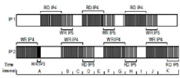
To focus on the efficiency evaluation of the crossbar bus architecture, we design an SOC system as shown in FIGURE 6 which contains two masters (IP1 and IP2) and three slaves (IP3, IP4 and IP5). In this experiment we compare the communication efficiency of the SOC systems with the shared bus architecture and the crossbar bus architecture. The transactions used in the experiment are described as follows.
1. Master IP2 first requests a series of burst WR transactions to slave IP4 and a WR transaction to slave IP3.
Int. J. Adv. Res. Sci. Technol. Volum e 3, Issue 4, 2014, pp.219-223. 3. Master IP1 then requests a series of burst WR
transactions to slave IP5, and master IP2 requests a series of burst WR transactions to slave IP4.
4. Master IP2 requests a series of burst RD transactions to slave IP5.
The procedure from step2 to step4 is iterated for 100 Iterations. The execution of these transactions on the crossbar architecture can be illustrated in FIGURE 7, where parallel communication between different masters and slaves happens in time intervals B, D, F, H and J. The behavior on the shared bus architecture is all in series without any parallel communication. Experimental results show that the proposed bus with crossbar interconnection reduces about 23.35% communication cycles as comparing to the tradition shared bus architecture such as AHB.
In the last experiment, we evaluate the efficiency of out-of-order transactions using the proposed scheduler. We assume that the access latency of the slave IP3 and IP4 in FIGURE 6 are 1 cycle and 3 cycles, respectively. The slave IP5 has the access latency of 5 cycles when it is accessed by master IP1 and two cycles when it is accessed by master IP2. In the simulation, IP1 first requests a series of out-of-order WR transactions, IP2 then requests a series of out-of-order RD transactions. After that, IP2 requests a series of out-of-order WR transactions, and IP1 finally requests a series of out-of-order RD transactions. The simulation results show that when each series of these requests contain 6000 transactions, the proposed scheduler reduces 67.16% communication cycles as comparing to a bus that supports only in -order transactions.
Conclusions:
The current trend of the bus standard is to define an explicit bus interface and leave the internal bus architecture to the bus designer. The design which complies with the bus interface protocol to carry out the various advanced bus functionality consequently dominates the communication efficiency of an SOC system. In this work, we develop an on-chip bus employing OCP as the bus interface. Various bus transactions defined in AXI and OCP to reduce the communication latency and increase the bus throughput are supported by the proposed bus architecture. Experimental results demonstrate the efficiency of the proposed bus in both simulation speed and execution performance.
Fig. 6: SOC system for bus evaluation
Fig. 7: Performance analysis of parallel transactions
References:
1. Advanced M icrocontroller Bus Architecture (AM BA) Specification Rev 2.0 & 3.0, http://www.arm.com. 2. Open Core Protocol (OCP) Specification,
http://www.ocpip.org/home.
3. Y.-T. Kim, T. Kim, Y. Kim, C. Shin, E.-Y. Chung, K.-M .Choi, J.-T. Kong, S.-K. Eo, “Fast and Accurate Transaction Level M odeling of an Extended AM BA2.0 Bus Architecture,” Design, Automation, and Test in
Europe, pages 138-139, 2005.
4. G. Schirner and R. Domer, “Quantitative Analysis of Transaction Level Models for the AMBA Bus,” Design,
Automation, and Test in Europe, 6 pages, 2006.
5. C.-K. Lo and R.-S. Tsay, “Automatic Generation of Cycle Accurate and Cycle Count Accurate Transaction Level Bus Models from a Formal Model,” Asia and
South Pacific Design Automation Conference, pages
558-563, 2009.
6. N.Y.-C. Chang, Y.-Z. Liao and T.-S. Chang, “Analysis of Shared-link AXI,” IET Computers & Digital
Techniques, Volume 3, Issue 4, pages 373-383, 2009.
7. IBM Corporation, “Prioritization of Out-of-Order Data Transfers on Shared Data Bus,” US Patent No.
7,392,353, 2008.
8. David C.-W. Chang, I.-T. Liao, J.-K. Lee, W.-F. Chen, S.-Y. Tseng and C.-W. Jen, “PAC DSP Core and Application Processors,” International Conference on
Multimedia andExpo, pages 289-292, 2006.