[Gomez* 6(1): January, 2019] ISSN 2349-4506
Impact Factor: 3.799
G
lobal
J
ournal of
E
ngineering
S
cience and
R
esearch
M
anagement
SEMICONDUCTOR PACKAGE DESIGN OPTIMIZATION FOR MITIGATION OF
DAF VOIDS AND DELAMINATION
Rammil A. Seguido, Frederick Ray I. Gomez
*
New Product Introduction Department, Back-End Manufacturing & Technology, STMicroelectronics,
Inc. Calamba City, Laguna, Philippines 4027
DOI: 10.5281/zenodo.2553461
KEYWORDS
:
Substrate package; substrate design; optimization; planarized; delamination; DAF voids; MSL3.ABSTRACT
This technical paper discusses the challenges encountered in the development of a compact and thinner package that incorporates multiple or stacked dice in one. For the case of this paper, Die1 (bottom die) is smaller than Die2 (top die) and must be the first one to be die bonded, making the internal construction an unbalanced stacked dice. Typically, stacked dice is in pyramid layout, wherein a single large bottom die supports smaller top die. Nonetheless, success is measured when there is a solution to control or mitigate die attach voids and eliminate or significantly minimize delamination for unbalanced stacked dice as mentioned. Ultimately, the paper presents the understanding of the factors involved and the package design optimization approach used to produce a successful unbalanced stacked die in a thin package using thin substrate.
INTRODUCTION
The increasing interest to incorporate several dice into a single molded Integrated Circuit (IC) package to get multiple desired functions has led to the development of multiple dice or stacked dice configuration of semiconductor IC package. Instead of separately mounting electronic components like analog ICs and digital ICs to the Printed Circuit Board (PCB), they can now be integrated into a single package.
In this study, the internal construction of the semiconductor package or device (hereinafter referred to as Device A) must be designed to stack smaller Die1 at the bottom and larger Die2 on top, as illustrated in Fig. 1. An interposer silicon die was added to support the top die overhang in Fig. 1. The stacked dice were supported by 0.13mm substrate and encapsulated with 0.42mm mold cap.
Fig. 1. Package cross-section with added interposer to support Die2 (top die) overhang
Actual evaluation of the first version of Device A, however, showed that there were issues of delamination between top and bottom dice, as well as die attach voids between bottom die and substrate. In order to resolve the issues encountered, factors involved in the delamination and voids were investigated and package design optimization focusing on substrate was carried out.
REVIEW OF RELATED LITERATURE
Stacked Dice using Die-Attach on Film (DAF) on Substrates
[Gomez* 6(1): January, 2019] ISSN 2349-4506
Impact Factor: 3.799
G
lobal
J
ournal of
E
ngineering
S
cience and
R
esearch
M
anagement
liquid-type die-attach material can be easily applied onto packaging with DAF. Process could be simplified by eliminating the dispensing and also skipping the post die attach cure. However, DAF void always is one of the major concerns, especially for its application between die and the substrate [7] [8]. Reliability issue of delamination likely occurs at the DAF-substrate interface [7] [9]. DAF void characteristics and its formation and reduction mechanism were then studied. Aside from die attach or diebonding parameters, many other factors are inevitable with regards to the void performance. For Device A, DAF voids between bottom dice (Die1 and interposer) and substrate were also considered as one of the contributors for the Die2 (top die) delamination issue.
Substrate Package Design Layout
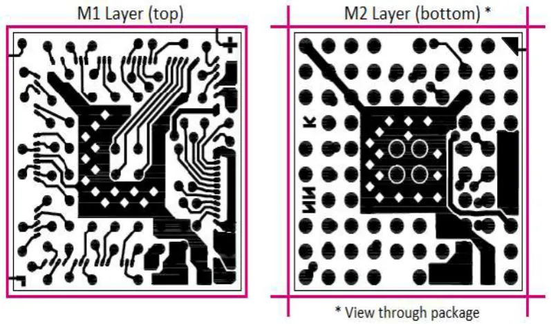
Substrate is normally constructed with metal planes to ensure Copper (Cu) balance and solder mask balance between layers to ensure no substrate delamination when subjected to reflow [9]. Electrical simulations in relation to the metal plane or metal strips in substrate should govern for resistance, inductance and capacitance. Fig. 2 shows the 2 layer (top side – M1 and bottom side - M2) construction of the substrate for Device A, with metal or copper balance of 16%. The substrate layout design is done using Cadence SiP Layout software [10], a computer-aided design (CAD) tool for wirebond, flip-chip, and wafer-level chip-scale packaging (WLCSP).
Fig. 2. Substrate design layout top and bottom view
METHODOLOGY
Substrate Design Modification and Package Modeling
[Gomez* 6(1): January, 2019] ISSN 2349-4506
Impact Factor: 3.799
G
lobal
J
ournal of
E
ngineering
S
cience and
R
esearch
M
anagement
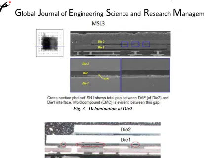
Fig. 3. Delamination at Die2
Fig. 4. DAF voids at Die1
With the results, a fault-tree analysis in Fig. 5 was then performed to prove the phenomenon that the ground plane expands after heat is applied.
Fig. 5. Fault-tree analysis
Correlation Between DAF Voids and Substrate Topology
[Gomez* 6(1): January, 2019] ISSN 2349-4506
Impact Factor: 3.799
G
lobal
J
ournal of
E
ngineering
S
cience and
R
esearch
M
anagement
Fig. 6. M1 metal trace of ground plane served as fulcrum, inducing voids and Die2 delamination
It can be observed that in every after metal plane, there is large void between die and substrate. Measurements of the peaks and valley were more than 10µm and DAF thickness is at 20µm. With this, DAF needs to fill the gap with depth equivalent with 50% of its thickness, which produces the challenge towards DAF gap filling capability. Therefore, these voids result from the insufficient gap and it can be explained that DAF voids have the properties of fixed position and similar pattern, which is matched with substrate surface topography.
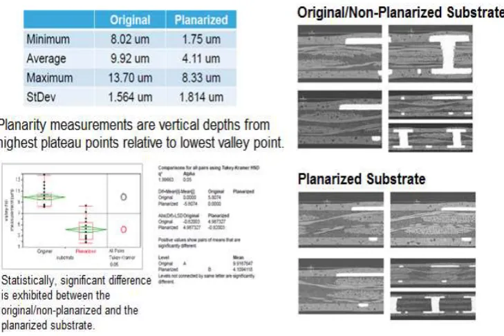
A comparison of the original or non-planarized substrate and the planarized substrate was performed to check the difference as shown in Fig. 7. Difference of more than 5 microns was observed.
Fig. 7. Comparison between non-planarized and planarized substrate
Substrate design Iterations
[Gomez* 6(1): January, 2019] ISSN 2349-4506
Impact Factor: 3.799
G
lobal
J
ournal of
E
ngineering
S
cience and
R
esearch
M
anagement
Table 1. Process evaluation matrixEvaluation
Run # DAF Evaluation
Substrate
(with variation) Remarks
1 Die1 and Die2 – rigid and thin (20µm)
Non-planarized – existing for Device A
Control Run: Samples should fail MSL3 to validate the issue (with cross section validation) 2
Die2 – softer and thicker DAF (30µm),
Die1 – rigid and thin (20µm)
Non-planarized – existing for Device A
Samples must pass MSL3 with cross section validation
3
Die2 – softer and thicker DAF (30µm),
Die1 – rigid and thin (20µm)
Planarized from other package
Response in time (0) with cross-section validation
DISCUSSION OF RESULTS
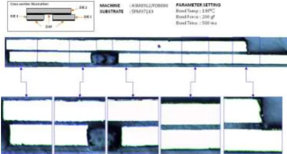
Reliability tests (MSL3) were done using a different DAF, this time softer and thicker DAF for Die2 (top die). Shown in Fig. 8 and 9 are the MSL3 results.
Fig. 8. MSL3 passed on assembly package performed using softer and thicker DAF for Die2
Fig. 9. Die attach stacked die using same rigid and thin DAF showed zero (0) voids for bottom dice at time zero
Results of the evaluation are summarized in Table 2. Based on the results, Die2 should use softer and thicker DAF while bottom dice (Die1 and interposer) should use rigid and thinner DAF on a planarized substrate.
Table 2. Summary of evaluation results
Evaluation Run # Results Remarks
1 Fail Previous issue replicated
2 Pass Passed MSL3
[Gomez* 6(1): January, 2019] ISSN 2349-4506
Impact Factor: 3.799
G
lobal
J
ournal of
E
ngineering
S
cience and
R
esearch
M
anagement
CONCLUSION AND RECOMMENDATIONS
Based on the study with the three evaluation runs completed, planarized substrate should be considered for DAF application. Die2 (top die) should use softer and thicker DAF to compensate variation of bottom dice. On the other hand, bottom dice (Die1 and interposer) should use rigid and thinner DAF to maintain level.
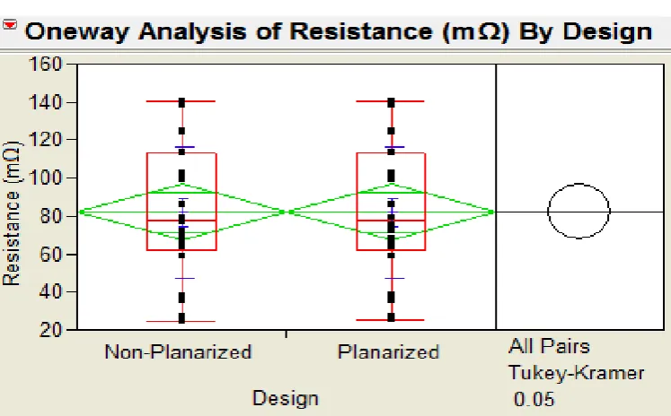
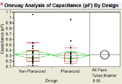
New substrate design for Device A proposal is shown in Fig. 10, replacing the metal plane in M1 with strip type metals and reducing M2 density resulted to better Cu balance [11]. Fig. 11-13 showed no significant difference in package electrical modeling performance for resistance, self-inductance and self-capacitance (summarized as RLC). SAS-JMP software [12] is used to determine if the two designs (non-planarized and planarized) have statistical difference in the RLC performance.
Fig. 10. Proposed substrate design with metal strip design
[Gomez* 6(1): January, 2019] ISSN 2349-4506
Impact Factor: 3.799
G
lobal
J
ournal of
E
ngineering
S
cience and
R
esearch
M
anagement
Fig. 12. Statistical comparison of 2 designs in terms of inductance
Fig. 13. Statistical comparison of 2 designs in terms of capacitance
Based on the results, it is highly recommended to optimize DAF selection and substrate design when developing stacked die. Since this study has just focused on substrate design to eliminate delamination and voids, it is also recommended that DAF selection should be considered to ensure robustness of material selection.
It is highly recommended that the assembly and test manufacturing processes and handling of Device A observe proper Electrostatic Discharge (ESD) controls. Controls and opportunities presented in [13] [14] could be very useful to help ensure ESD check and controls.
ACKNOWLEDGMENTS
The authors would like to thank the New Product Introduction team and colleagues of STMicroelectronics Calamba who have contributed to the Device A package development, especially to E. Angeles who first handled the project. E. Angeles already pursued another direction to his career outside ST. Finally, the authors would like to extend great appreciation to the ST Calamba Management Team.
REFERENCES
1. R. Doering, and Y. Nishi, “Handbook of semiconductor manufacturing technology,” 2nd ed., USA: CRC Press, July 2007.
[Gomez* 6(1): January, 2019] ISSN 2349-4506
Impact Factor: 3.799
G
lobal
J
ournal of
E
ngineering
S
cience and
R
esearch
M
anagement
3. C. Chew, and C. K. Tan, “Substrate design and process optimization of LGA (BT-based) package,” International Conference on Electronic Materials and Packaging, pp.1-10, Toronto, Canada, December 2006.
4. W. J. Greig, “Integrated circuit packaging, assembly and interconnections,” 1st ed. USA: Springer, March 2007.
5. S. N. Song, H. H. Tan, and P. L. Ong, “Die attach film application in multi die stack package,” 7th Electronics Packaging Technology Conference, vol. 2, pp. 848-852, Singapore, December 2005. 6. C. L. Chung, S. L. Fu, T. Lin, A. Lu, M. Ho, D. Kuo, and S. Chou, “A study on the characteristic of UV
cured die-attach films in stack CSP (chip scale package),” 12th IEEE International Conference on Microelectronics, pp. 365-368, Cairo, Egypt, December 2003.
7. Y. Su, D. Bai, V. Huang, W. Chen, and T. S. Xian, “Effect of transfer pressure on die attach film void performance,” 11th Electronics Packaging Technology Conference, pp. 754-757, Singapore, December 2009.
8. I. Ahmad, N. N. Bachok, N. C Chiang, M. Z. M. Talib, M. F. Rosle, F. L. A. Latip, and Z. A. Aziz, “Evaluation of different die attach film and epoxy pastes for stacked die QFN package,” 9th Electronics Packaging Technology Conference, pp. 869-873, Singapore, December 2007.
9. E. Angeles, R. Seguido, and F. R. Gomez, “Elimination of voids and delamination in unbalanced stacked dice by optimizing substrate design,” 23rd ASEMEP National Technical Symposium, Manila, Philippines, June 2013.
10. Cadence Design Systems, Inc., “IC package design and analysis – SiP layout”,
https://www.cadence.com/content /cadence-www/global/en_US/home/tools/custom-ic-analog-rf-design/circuit-design.html
11. R. Seguido, F. R. Gomez, and E. Angeles, “Support structure for stacked integrated circuit dies,” US Patent No. US9258890B2, February 2016.
12. SAS Institute Inc., “JMP statistical discovery software”, https://www.jmp.com/en_ph/software.html
13. F. R. Gomez and T. Mangaoang Jr., “Elimination of ESD events and optimizing waterjet deflash process for reduction of leakage current failures on QFN-mr leadframe devices,” Journal of Electrical Engineering, David Publishing Co., vol. 6, no. 4, pp. 238-243, July 2018.