Automatic Compensation Device for Distribution Line
Based on Wireless Sensor
https://doi.org/10.3991/ijoe.v13i05.7058
Chunmei Liu
Shenyang University of Technology, Shenyang, China [email protected]
Guohong Shi
China Petroleum Liaoyang Petrochemical Industries Co nylon factory, Liaoyang, China
Abstract—The purpose is to solve the problem that the automatic compen-sation device of the distribution line is too scattered. A power supply line auto-matic compensation device based on the wireless sensor network is proposed. The device data acquisition terminal adopts electromagnetic induction power supply and open wireless transmission design, without disconnecting the line threading and secondary lead to the controller. A more mature microcontroller is used as a controller, and it is combined with more advanced control algorithm and the reactive power of the electrical equipment in time, so as to detect and calculate the number of capacitor banks required for compensation. Based on the design of wireless sensor network, through the computer for real-time moni-toring,the difficulties of promoting the automatic compensation of distribution lines due to the inconvenience of centralized operation and management have been overcome. In conclusion, the automatic compensation device can improve the quality of power supply and promote the development of China's electric power industry as long as it is continuously improved and perfected.
Keywords—wireless sensor, distribution line, automatic compensation
1
Introduction
overcome the difficulty of promoting the automatic compensation of distribution lines due to the inconvenience of centralized operation and management.
At present, low-voltage "local automatic compensation" has been popularized in 100kVA and above distribution transformers [1]. However, in less than 100kVA transformer, we generally do not install the "local automatic compensation" device, especially in the rural irrigation, the line is longer, and the single transformer capacity is smaller [2]. Therefore, the automatic compensation device that we designed in this paper is a non-power automatic compensation device, which can make up the defi-ciency of "local automatic compensation" on l0kVA distribution line and improve the utilization rate of automatic compensation equipment. Automatic compensation of reactive power in the distribution line is not only beneficial to reduce the line loss, but also conducive to operation and management [6].
2
State of the art
The early reactive power compensation device uses a synchronous modulator. It is specifically used to generate reactive power synchronous motor. In the case of over-excitation or under-over-excitation, it can be issued in different sizes of capacitive or in-ductive reactive power. In recent decades, synchronous camera plays a major role in the power system reactive power control. However, because it is a rotating motor, the loss and noise are large, the operation and maintenance are complex, and the response is slow, it has been unable to adapt to the requirements of fast reactive power control in many cases.
Since the 1970s, there has been a static reactive power compensation technology. The so-called static reactive power compensation refers to the use of different static switch switching capacitor or reactor, so that it has the ability to absorb or send reac-tive current. It can be used to improve the system power factor, stable system voltage and so on.
At present, it is one of the main indexes to measure the performance of distribution network to install outdoor reactive power compensation. In Japan, the automatic switching rate of the outdoor compensation capacitor for the distribution network system has reached 86.4%. In the United States, many city roads along the road poles are equipped with parallel capacitor group, and it uses automatic device control.
energy. However, its installation is too scattered, and a single capacity is small, so it is difficult to promote in a wide range.
In this paper, we design a wireless sensor network based on the distribution line re-active power device, and its main innovations are:
1. The utility model adopts the high voltage cable suspension electromagnetic
in-duction communication power supply, which has the advantages of high integra-tion, small size, light weight and high degree.
2. use the open wireless transmission design to solve a lot of difficulties, for
exam-ple, the conventional sampling module installation is not convenient, it has to dis-connect the line, and the second must lead to the controller and other issues.
3. Based on the design of wireless sensor network, through the computer for
real-time monitoring, we have overcome the difficulty of promoting the automatic compensation of distribution lines due to the inconvenience of centralized opera-tion and management.
The reactive power automatic compensation device based on wireless sensor net-work has the following functions:
1. We carry out the real-time detection on the operating parameters of the
distribu-tion network, and use advanced control theory to calculate the number of switching capacitors.
2. The data acquisition module is powered by an electromagnetic induction power
supply of the power cable and can be used for opening wireless transmission. The utility model has the advantages of convenient installation, no need to disconnect the line and no need of the secondary lead to the controller.
3. There is power memory function. When the power is turned off, the parameters
and procedures of automatic memory are never lost. In the transmission, the com-pensator is still in accordance with the original user to set the parameters and pro-gram operation control.
4. Based on the design of wireless sensor network, through the computer for
real-time monitoring, to overcome the difficulty of promoting the automatic compensa-tion of distribucompensa-tion lines due to the inconvenience of centralized operacompensa-tion and management.
detect and calculate the number of capacitor banks required for compensation. Based on the design of wireless sensor network, through the computer for real-time monitor-ing, we have overcome the difficulty of promoting the automatic compensation of distribution lines due to the inconvenience of centralized operation and management.
3
Methods
3.1 System hardware design
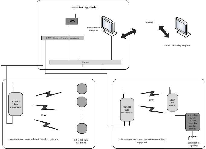
The structure of the reactive power compensation device schematic is as shown in Figure 1, and it is mainly composed of a monitoring computer, information processor, data concentrator, data acquisition, switching equipment and so on.
The type of MSD.311 data collector is electromagnetic induction terminal equip-ment with real-time data acquisition and processing functions, and can complete the collection and transmission of current and voltage under the supervision of SDS data concentrator. This part is the main work of this article, and it will be described in detail later.
The thyristor control capacitor (TSC) is used by the MSD.321 terminal to receive the switching signal from the SDS.011 type data concentrator, and then trigger the thyristor control capacitor group to complete the reactive power compensation.
GPS
IPC-012 type information processor
Ethernet
monitoring center
local detection computer
Internet
remote monitoring computer
SDS-011 data concentrator
SRW
MSD-311 data acquisition
substation transmission and distribution bus equipment
SDS-011 data concentrator
MSD-321 terminal
low voltage thyristor
silicon controlled
rectifier module
controllable capacitors substation reactive power compensation switching
equipment SRW
Design of MSD-311 Data Collector: The main functions of the MSD.3ll type data acquisition device are as follows: through the current transformer (CT) and the capac-itance voltage probe, the parameters related to the power factor of the network are detected from the power grid, which is transmitted to the MSP430FE427 processor. After the processor calculates the relevant grid parameters, the control wireless transmission module transfers the data to the SDS.011 data concentrator. The hard-ware structure of MSD.311 data collector is mainly: MSP430 processor, electromag-netic induction power supply, current transformer (CT), capacitive voltage probe and wireless communication module SRW401 / 2401 Module. The block diagram is shown in Figure 2.
capacitive voltage
probe CSV-IV current transformer
MSP430 processor
SRW401/240 1 Module induction power supply electromagnetic
frequency
measurement conversiontrue RMS
Fig. 2. Structure of MSD-311 data acquisition system
(1). Design of electromagnetic induction power supply
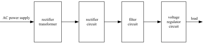
The MSD-311 data acquisition device adopts the line current sensing energy sup-ply mode. The energy of the power supsup-ply comes from the high voltage line. Through the high voltage line on the take-in coil, make the high-voltage line energy converse to the secondary side, so as to achieve isolation power supply. Through the coil from the high-voltage cable to induce the exchange of energy, it needs to pass through the DC voltage regulator circuit to convert the AC energy into the energy needed to measure the device.
The electromagnetic induction power supply consists of four parts, they are rectifi-er transformrectifi-er, rectifirectifi-er circuit, filtrectifi-er circuit and voltage regulator circuit, the block diagram is shown in Figure 3.
rectifier
transformer rectifier circuit circuitfilter
voltage regulator
circuit
AC power supply load
(2). Current acquisition unit design
In the whole system design, the collection is the focus, the accuracy of the acquisi-tion is directly related to the overall performance of the system. The device uses MELEXIS CSA.IV Hall current sensor, compared with the traditional Hall sensor and magnetoresistive sensor, the sensitivity of the CSA.1V Hall sensor is comparable to that of the magnetoresistive sensor, which is up to 300 V / T. At the same time, the CSA.IV Hall sensor also improved the magnetoresistive sensor nonlinearity and hys-teresis.
The current acquisition circuit of the device will be put the Hall sensor CSA.1V package on the core of the surface, the supply voltage is 5V, the sampled current signal is input from the interface J2, and the magnetic beads and 1K protection resis-tor are followed by the KMSP430FE427 chip 11+ and 11- two pins. Diode D1, D2, D3, D4 is to ensure that the chip pin absolute voltage in the allowable range, and will not damage the chip.
(3). Voltage acquisition unit design
The voltage acquisition circuit is mainly through the voltage transformer to convert the high voltage into a low voltage, after a series of signal conditioning, and finally input to the processor for processing. This system uses the PT204A voltage trans-former, the input voltage through the current limiting resistor R ', so that the PT204A voltage transformer primary rated current is 2mA (or user defined a reasonable value), and the secondary will produce an identical current. By the operational amplifier, the user can conveniently obtain the desired voltage output by adjusting the value of the feedback resistor R. However, the capacitance C and the adjustable resistance r are used to compensate for the phase shift, and if the phase shift is not required, the ca-pacitor C and the adjustable resistor r may not be connected. IC is a general-purpose operational amplifier, the use of superior performance of the operational amplifier can achieve higher accuracy and better stability, the power supply voltage can be custom-ized according to specific circumstances.
(4). MSP430 processor
This device uses MSP430FE427 as a MCU for the MSP430 series, which inherits the ultra low power consumption and high integration of the MSP430 system. It has 16 capture / compare registers with 16-bit timer A, Timer- A and the serial communi-cation interface (USART), through the software to the select functions of asynchro-nous USART or synchroasynchro-nous SPI communication. At the same time, MSP430FE427 also has a programmable level detection power supply voltage management and monitoring, and the basic timer to support real-time clock function.
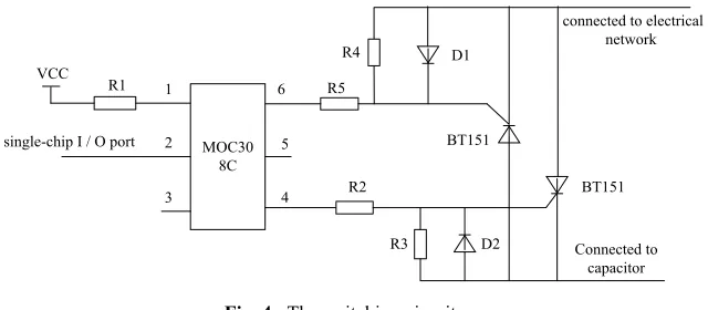
trigger voltage, at this point, it will make one of the conduction, so as to achieve the purpose of zero voltage conduction. The schematic diagram is shown in Figure 4.
MOC30 8C
VCC R1
1
2
3
6
5
4 single-chip I / O port
R5 R4
R2
R3 D2
BT151
BT151 D1
Connected to capacitor connected to electrical
network
Fig. 4. The switching circuit
The design of serial communication circuit: In order to improve the reliability of serial communication, enhance the anti-jamming ability and increase the transmission distance, it is necessary to use the standard serial bus interface to convert the input and output level of the serial port [7]. The serial communication module mainly real-izes the communication between the central node and the monitoring computer [8]. On the one hand, the data processed by the central node is transmitted to the monitor-ing computer, and on the other hand, the switchmonitor-ing module is operated accordmonitor-ing to the control command of the monitoring computer. In order to achieve multiple mod-ules simultaneously access to the temperature monitoring system, the module serial communication unit designed the standard RS485 bus interface. This design uses the RS485 serial communication interface standard differential balanced wire circuit, the anti-interference ability is strong, the receiver can be as low as 200mV signal detec-tion, and the transmission data can be recovered from the thousands of kilometres, so it is especially suitable for long distance communication.
3.2 System software design
The main function of the reactive power compensation device software is: The voltage and current signals are sampled and processed, and the real-time data is stored in RAM. The real-time data is uploaded to the data concentrator through the wireless module, after the information processing analysis and calculation as the reactive pow-er compensation switching capacitor bank switching decision, and then use the wire-less module to send to the switching terminal, through the thyristor control switching capacitor group, to complete the task of compensation.
storage, authentication and management of high voltage power grid related data (cur-rent, voltage, power factor, etc.) and supports WEB access. The software has a simple user interface, completes the parameters collection of the distribution network current, voltage, active power, power factor, reactive power and so on, while calculates the needs of capacitor switching, and makes switching decisions.
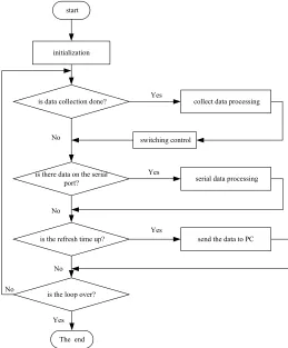
Since the object to be processed by this system is a periodic voltage and current signal, it is determined that the frame of the main program is a cyclic process. The main program is responsible for the integration of the various functional modules into an organic whole, and to achieve a reasonable scheduling between the various func-tional modules. It is the first to complete the initialization of the entire system, after the initialization, the system is get into the main loop, the main program in the main loop through the query function of each function to determine whether the need to enter the appropriate module for processing. After each module completes its own task, through the method of changing the flag to notify the main program, it can con-tinue to carry out the next step. The main program flow chart is shown in Figure 5.
is data collection done? start
initialization
is there data on the serial port?
is the refresh time up?
is the loop over?
The end
collect data processing
switching control
serial data processing
send the data to PC Yes
No
Yes
Yes No
No
Yes No
3.2.2 Data acquisition program design: Data acquisition is mainly to simulate the frequency, voltage and current. After the voltage and current of the power grid through the signal conditioning circuit, it is get into the MSP430FE427 microcontrol-ler Il, U1 input port for processing. First of all, we have to initialize the settings of MSP430FE427 microcontroller ESP module of some registers. The initialization of the ESP module mainly includes: simulate the initialization of the front register and the initialization of the parameter register (via the mailbox operation). Analog front-end initialization includes: select the AD sampling clock source, the clock division factor, the reference voltage, the preamplifier amplifier magnification, and the over-sampling rate [5]. When a measurement is completed, the ESP returns the result of each measurement to the result return register and sends a message to the CPU via the mailbox informing the CPU to read the data.
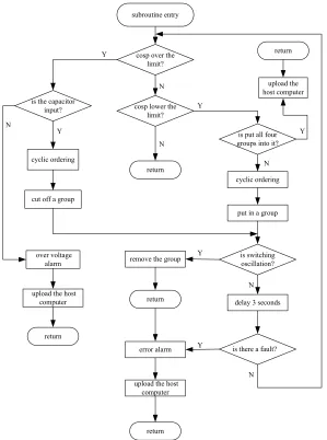
The design of switching judgment program: Reactive power compensation is through the control capacitor switching to compensate for the grid, so that the grid running is in a stable and healthy state. Therefore, the capacitive switching design is reasonable or not directly related to the reliability of the entire system and stability. The basic idea of the subroutine design is to set the time interval to enter the subrou-tine, thus to determine whether the over voltage, and make phase judgment, as well as carry out the comprehensive switching to the power factor of the upper and lower limits. In the process of charging the capacitor, the value is taken out by comparing the value in the capacitor running time unit, and the switch is cut from the shortest running time. During the cutting process, it is cut off from the longest running time to realize "cyclic switching". In order to ensure that the switch is a loop, there must be a circular queue, and the number of elements in the queue depends on the number of user sets. In addition, there is a need to put a pointer and cut the pointer, they are directed to the capacitor group that will be put into operation, and it will cut the elec-trical group. The flow chart of the cut-off judgment procedure is shown in Figure 6.
3.3 The design of wireless sensor network platform
The wireless sensor network platform design of the device mainly involves three aspects: the sensor node platform, the central node platform and monitoring manage-ment platform.
The sensor node constitutes the support platform of the physical layer of the wire-less sensor network. It consists of the data acquisition module, the processor module, the wireless communication module and the power module. The main functions of the data acquisition module, data processing module and power module have been intro-duced. The main function of the wireless transceiver module is that it is responsible for wireless communication with the central node, exchanging control messages and collecting and collecting data.
special gateway device with no monitoring function with a wireless communication interface.
The monitoring management platform consists of one or more computers located in the main control room, which is responsible for monitoring and managing the en-tire sensor network. The center nodes or sensor nodes to increase or decrease, the management platform needs to be reflected. When the node power factor is abnormal, the monitoring computer also reacts immediately. All collected data can be stored and displayed in real time to monitor the computer, so that managers can make timely processing.
upload the host computer subroutine entry
cosp over the limit?
cosp lower the limit?
return is the capacitor
input?
cyclic ordering
cut off a group
return
is put all four groups into it?
cyclic ordering
put in a group
over voltage alarm
upload the host computer
return
is switching oscillation?
delay 3 seconds
is there a fault? remove the group
return
error alarm
upload the host computer
return
N N
N
Y
Y
N
N
Y Y N
Y
Y
4
Experiment
Due to the limitation of the condition, it is impossible to carry on the simulation experiment of high voltage field. According to the basic theory of electromagnetic induction, it can only satisfy the condition of high current.
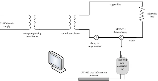
(1). Build test platform
The current acquisition accuracy measurement simulation platform is shown in Figure 7, The main components are voltage regulator, control transformer, copper, cable, adjustable load, MSD-031 data collector, SDS-011 data concentrator and IPC-012 information processor. Here the voltage regulator transformer output voltage is OV-250V, the maximum output power is 5000W, control transformer output voltage is 3V, and the adjustable load is copper or copper and so on. The platform work flow is to input 220V single-phase AC power to the regulator, modulate the output voltage and then input to the control transformer, and adjust the output current by changing the load size. The adjustable voltage regulator can make the power core output a wide range of current from 0 to 1200A, and the maximum power of the circuit is 3600W, so as to ensure the safety of the regulator transformer work. In the test, the data acqui-sition module is fixed on the cable segment, as far as possible to simulate the working environment. A large range of clamp ammeter is used on the cable to measure the size of the cable current. The current value is collected by the MSD-031 data collector, sent to the SDS-011 data concentrator through the wireless module, and then passed to the information processor through the RS485 bus to read the current parameters.
A
SDS-011 data concentra
tor 220V electric
supply
voltage regulating
transformer control transformer
copper line
MSD-031 data collector
clamp on amperemeter
IPC-012 type information processor
adjustable load
cable
Fig. 7. Current acquisition accuracy test platform
(2). Measurement results and data analysis
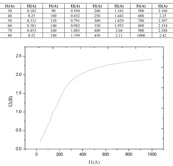
the data concentrator. Finally, the MELEX's CSV-1V Hall sensor is selected as the current acquisition chip, and the sensor is affixed to the inner surface of the power core to obtain the ideal data, as shown in Table l. Il is the bus current measured by the clamp ammeter, and 12 is the Hall sensor output current.
The data in Table 1 is converted into a matlab curve, as shown in Figure 8.
Table 1. Hall sensor test data
I1(A) I2(A) I1(A) I2(A) I1(A) I2(A) I1(A) I2(A) 30 0.182 90 0.594 200 1.343 500 2.166 40 0.25 100 0.652 250 1.643 600 2.25 50 0.312 120 0.791 300 1.829 700 2.307 60 0.381 140 0.982 350 1.953 800 2.354 70 0.453 160 1.083 400 2.04 900 2.388 80 0.52 180 1.199 450 2.11 1000 2.42
Fig. 8. The relationship between the bus current and output current
5
Conclusion
In this paper, we design the automatic compensation of reactive power based on wireless sensor network, and complete the hardware and software design of the de-vice, which is based on the problem that the reactive power compensation device of the existing distribution line is too loose and is not conducive to the operation and management. At last, we carry out the sampling of the grid parameters and the wire-less communication experiment. In the process of research, it is found that the auto-matic compensation device designed in this paper can be further studied in the follow-ing aspects: (1) From a sfollow-ingle reactive power compensation, it is developed to a filter with a harmonic suppression function of the compensation device. (2) As the reactive power control is a multi input/ multi output closed-loop control system in the optimal control problem, and the system is subject to many factors. Sometimes, the power factor cannot reach the best performance, and it can only change within the range of satisfaction. (3) To achieve the switching from the thyristor switching circuit to the use of IGBT and other voltage-controlled to control the capacitor group. Undoubted-ly, it has various flaws, so it needs to be continuously improved and perfected in later researches. Only in this way can it improve the quality of power supply and promote the development of China's electric power industry.
6
References
[1]Bai R. (2016). Design and installation of 10kV power distribution line reactive power au-tomatic compensation device[J]. Electronic Test, 13(1), 32-45.
[2]Han, S., Gong, Z., Meng, W., Li, C., Zhang, D., & Tang, W. (2016). Automatic Precision Control Positioning for Wireless Sensor Network. IEEE Sensors Journal, 16(7), 2140-2150. https://doi.org/10.1109/JSEN.2015.2506166
[3]Kong J, Meng H. (2016). Application of GWBH reactive power automatic compensation device in the distribution line[J]. Electronic Test, 6(2), 79-102.
[4]Munir S, Li Y W. (2013). Residential distribution system harmonic compensation using PV interfacing inverter[J]. IEEE Transactions on Smart Grid, 4(2): 816-827. https://doi.org/10.1109/TSG.2013.2238262
[5]Saradva, P. M., Kadivar, K. T., Pandya, M. H., & Rana, A. J. (2016, April). Reactive and real power compensation in distribution line using D-STATCOM with energy storage. In Computation of Power, Energy Information and Commuincation (ICCPEIC), 2016 Inter-national Conference on (pp. 726-732). IEEE. https://doi.org/10.1109/iccpeic.2016.7557316 [6]Somov A, Karpov E F, Karpova E, et al. (2015). Compact low power wireless gas sensor
node with thermo compensation for ubiquitous deployment[J]. IEEE Transactions on In-dustrial Informatics, 11(6): 1660-1670. https://doi.org/10.1109/TII.2015.2423155
[7]Voronov G. (2015). Image capture devices configured to generate compensation gains based on an optimum light model and electronic apparatus having the same[J]. 25(7):1864-1875.
7
Authors
Chunmei Liu is with Shenyang University of Technology, Shenyang, China ([email protected]).
Guohong Shi is with China Petroleum Liaoyang Petrochemical Industries Co ny-lon factory, Liaoyang, China