RF Transceiver Module
Applications
o Ultra low power wireless Transceiver
o 433/868/915 and 2400 Mhz ISM/SRD band systems
o Consumer Electronics
o Wireless audio
o Alarm and security systems
o Home and building automation
o Wireless sensor networks
o Industrial monitoring and control
o Low power Telemetry
Product Description
The BITxxRT is a very low cost transceiver module designed for very low power wireless applications.
This module is intended for ISM (Industrial, Scientific and Medical) and SRD (Short Range Device) frequency band at 433, 868/915 and 2400 Mhz., but can easily be programmed for operation at other frequencies:
BIT04RT 400 – 464 Mhz BIT08RT 800 – 928 Mhz BIT24RT 2400 – 2483 Mhz
The Transceiver module supports various modulation formats and has a configurable data rate up to 500 kbps. The communication range can be increased by enabling a Forward Error Correction option, which is integrated in the module.
BITxxRT provides extensive hardware
support for packet handling, data buffering, burst transmissions, clear channel assessment, link quality indication and wake-on-radio.
The main operating parameters and the 64-byte transmit/receive FIFOs of
BITxxRT can be controlled via an SPI
interface. In a typical system, the
BITxxRT will be used together with a
microcontroller.
BITxxRT has a very small package
only 20 x 20 mm ready for both PTH and SMT assembly.
BITxxRT is based on the well-proven
CC1101 (BIT04RT and BIT08RT),
CC2500 (BIT24RT) Chipcon Products
from Texas Instruments.
Key Features
o Small size (20 x 20 mm package, 12 pins).
1. BIT04RT 400 – 464 MHz 2. BIT08RT 800 – 928 MHz
Features (continued from front page)
o High sensitivity (-110 dbm at 1.2 kpbs, 1% PER at 433 and 868 Mhz and –106 dbm at 2.4 kbps, 1% PER at 2,4 Ghz).
o Programmable output power up to + 10 dBm for BIT04RT/BIT08RT and +1 dBm for BIT24RT.
o Low current consumption (15,4 mA in RX,1,2 kbps,433 Mhz and 13,3 mA in RX, 250 kbps,input 30 dB above sensitivity limit)
o Excellent receiver selectivity and blocking performance.
o Programmable baseband modem.
o Ideal for multi-channel operation.
o Configurable packet handling hardware.
o Suitable for frequency hopping systems due to a fast settling frequency synthesizer.
o Optional Forwad Error Correction with interleaving.
o Separate 64-byte RX and TX data FIFOs
o Efficient SPI interface: All registers can be programmed with one “burst” transfer.
o Digital RSSI output.
o Programmable data rate up to 500 kbps
o BIT04RT/BIT08RT suited for system compliant with EN 300 220 (Europe) and FCC CFR Part 15 (US).
o BIT24RT suited for system
o Lead-free “green package.
o OOK/ASK, FSK, GFSK e MSK supported.
o Wake-on-radio functionality for automatic low –power RX polling.
o Flexible support for packet oriented systems: On chip support for sync word detection, address check, flexible packet length and automatic CRC handling.
o Programmable channel filter bandwidth.
o Automatic Frequency Compensa-tion can be used to align the frequency synthesizer to the received centre frequency.
o Many powerful digital features allow a high-performance RF system to be made using an inexpensive microcontroller.
o Optional automatic whitening and dewhitening of data.
o Support for asynchronous transparent receive/transmit mode for backwards compatibility with existing radio communication protocols
o Programmable Carrier Sense indicator
o Programmable Preamble Quality Indicator for detecting preambles and improved protection against sync word detection in random noise.
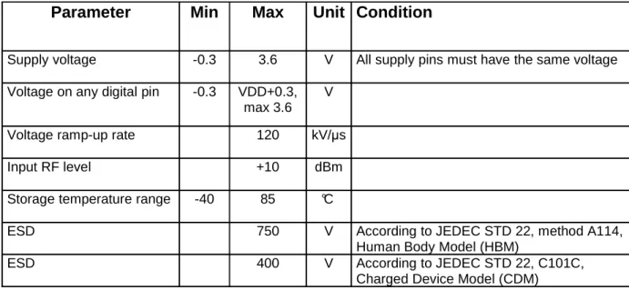
1. Absolute Maximum Ratings
Under no circumstances must the absolute maximum ratings given in Table 1 be violated. Stress exceeding one or more of the limiting values may cause permanent damage to the device.
Parameter Min Max Unit Condition
Supply voltage -0.3 3.6 V All supply pins must have the same voltage Voltage on any digital pin -0.3 VDD+0.3,
max 3.6 V
Voltage ramp-up rate 120 kV/µs
Input RF level +10 dBm
Storage temperature range -40 85 °C
ESD 750 V According to JEDEC STD 22, method A114,
Human Body Model (HBM)
ESD 400 V According to JEDEC STD 22, C101C,
Charged Device Model (CDM)
Table 1: Absolute Maximum Ratings
2. Operating Conditions
The operating conditions for BITxxRT are listed Table 2 in below.
Parameter Min Max Units Condition
Operating temperature -30 85 °C
Operating supply voltage 1.8 3.6 V All supply pins must have the same voltage
Table 2: Operating Conditions
3. Pin-Out
Pin # Pin Name
Pin Type Descrizione
P1 NC NC
P2 SI Digital Input Serial configuration interface, data input
P3 SCLK Digital Input Serial configuration interface, clock input
P4 SO
GDO1
Digital Output Serial configuration interface, data output Optional general output pin when CSn in High
P5 GDO2 Digital Output Digital Output pin for general use:
• Test signal
• FIFO status signals
• Clear Channel Indicator
• Clock output, down-divided from XOSC
• Serial output RX data
P6 GDO0 Digital I/O Digital Output pin for general use:
• Test signal
• FIFO status signals
• Clear Channel Indicator
• Clock output, down-divided from XOSC
• Serial output RX data
• Serial input TX data Also used as analog test I/O for prototype/production testing
P7 CSn Digital Input Serial configuration interface, chip select
P8 VDD Power 1.8V – 3.6V analog power supply connection
SISC L K SO GDO2 GDO0 C Sn AGND ANT AGND
4. Typical application
source code is avalaible on the web for this typical application.
BITxxRT
5.1. Technical Documents:
Data sheet CC1101 or CC2500 available for download from
http://www.chipcon.com or http://www.ti.com/lpw
5.2. Configuration Software
BITxxRT can be configured using the SmartRF® Studio software, available for download from http://www.chipcon.com or http://www.ti.com/lpw The SmartRF® Studio software is highly recommended for obtaining optimum register settings, and for evaluating performance and functionality. A screenshot of the SmartRF® Studio user interface for CC1101 is shown in Figure
6. Package Description
7. Recommended Footprint
The area underneath the module should be covered with solder resist in order to prevent short circuiting the test pads on the back side of the module. A solid ground plane is preferred.
BITxxRT
1.93 2.03 5.08 19 millime tri 76 L 80 b 200 p 746 A milsp
E
E
3.05 2.28 5.08 20.7 millime tri 120 H 90 w 200 p 816 E milsH
w
A
A
rL
rp
b
8. PACKAGING INFORMATION
Orderable device Status Package Type Pins Package Qty Eco Plan MSL Peak TempBIT04RT ACTIVE MLF 12 84 Green (RoHS
& no Sb/Br)
Level-2-260C-1 YEAR
BIT08RT ACTIVE MLF 12 84 Green (RoHS
& no Sb/Br)
Level-2-260C-1 YEAR
BIT24RT ACTIVE MLF 12 84 Green (RoHS
& no Sb/Br)
Level-2-260C-1 YEAR
9. General Information
9.1. Disclaimer
B.I.T. srl believes the information contained herein is correct and accurate at the time of this printing. However, B.I.T. srl reserves the right to make changes to this product without notice. B.I.T. srl does not assume any responsibility for the use of the described product; neither does it convey any license under its patent rights, or the rights of others. The latest updates are available at the BIT website or by contacting BIT directly.
As far as possible, major changes of product specifications and functionality, will be stated in product specific Errata Notes published at the BIT website. Customers are encouraged to sign up to the Developers Newsletter for the most recent updates on products and support tools.
Compliance with regulations is dependent on complete system performance. It is the customer’s responsibility to ensure that the system complies with regulations.
9.2. Life Support Policy
This BIT product is not designed for use in life support appliances, devices, or other systems where malfunction can reasonably be expected to result in significant personal injury to the user, or as a critical component in any life support device or system whose failure to perform can be reasonably expected to cause the failure of the life support device or system, or to affect its safety or effectiveness. B.I.T. srl customers using or selling these products for use in such applications do so at their own risk and agree to fully indemnify B.I.T. srl for any damages resulting from any improper use or sale.